Neamen D. Microelectronics: Circuit Analysis and Design
Подождите немного. Документ загружается.


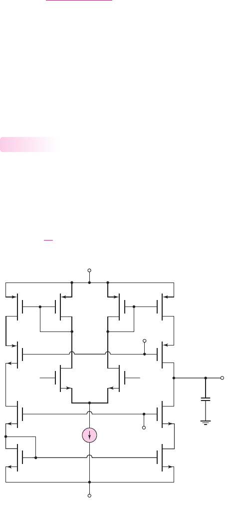
If a differential-mode input voltage is applied, then ac currents are induced in the
differential pair as shown in the figure. The ac current in M
1
flows through M
6
to the
output. The ac current in M
2
flows through M
5
and is induced in M
8
by the current-
mirror action of the active load. From previous work on diff-amps, the differential-
mode voltage gain is
A
d
= g
m1
(R
o6
R
o8
)
(13.41)
where
R
o8
= g
m8
(r
o8
r
o10
)
(13.42(a))
and
R
o6
= g
m6
(r
o6
)(r
o4
r
o1
)
(13.42(b))
We may note that we are neglecting the body effect. Normally the substrates
of all NMOS devices are tied to
V
−
and the substrates of all PMOS devices are tied
to
V
+
.
EXAMPLE 13.11
Objective: Determine the differential-mode voltage gain of the folded cascode diff-
amp in Figure 13.17.
Assume circuit and transistor parameters: I
REF
= 100
μ
A,
k
n
= 80 μA/V
2
,
k
p
= 40 μA/V
2
,
(W/L) = 25
, and
λ
n
= λ
p
= 0.02 V
−1
.
Solution: The transconductances are determined to be
g
m1
= g
m8
= 2
k
p
2
·
W
L
· I
D
= 2
40
2
· (25)(50) = 316 μA/V
and
g
m6
= 2
k
n
2
·
W
L
· I
D
= 2
80
2
· (25)(50) = 447 μA/V
The transistor output resistances are found to be
r
o1
= r
o6
= r
o8
= r
o10
=
1
λI
D
=
1
(0.02)(50)
= 1M
and
r
o4
=
1
λI
D4
=
1
(0.02)(100)
= 0.5M
The composite output resistances can be determined as
R
o8
= g
m8
(r
o8
r
o10
) = (316)(1)(1) = 316 M
and
R
o6
= g
m6
(r
o6
)(r
o4
r
o1
) = (447)(1)(0.51) = 149 M
The differential-mode voltage gain is then
A
d
= g
m1
(R
o6
R
o8
) = (316)(149316)
∼
=
32,000
978 Part 2 Analog Electronics
nea80644_ch13_947-1008.qxd 6/23/09 1:59 PM Page 978 pmath DATA-DISK:Desktop Folder:23/06/09:MHDQ134-13:

Comment: This example shows that very high differential-mode voltage gains can
be achieved in a folded cascode CMOS circuit. In actual circuits, the output resis-
tances may be limited by leakage currents so the very ideal values may not be realiz-
able. However, substantially higher differential-mode voltage gains can be achieved
in the folded cascode configuration than in the simpler diff-amp circuits.
EXERCISE PROBLEM
Ex 13.11: Assume the reference current in the folded cascode circuit shown in
Figure 13.17 is
I
REF
= 50 μ
A. Assume the transistor parameters are the same
as given in Example 13.11. Determine the differential-mode voltage gain.
(Ans.
∼
=
64,000
)
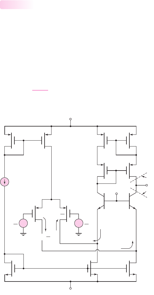
CMOS Current-Mirror Operational Amplifier Circuit
Another CMOS op-amp circuit is shown in Figure 13.18. The differential pair is
formed by M
1
and M
2
. The induced ac currents from these transistors drive transis-
tors M
3
and M
4
, which are the inputs of two current mirrors with a current multipli-
cation factor B. The current output of M
5
is then induced in M
8
by the current-mirror
action of M
7
and M
8
. The output signal currents then have a multiplication factor B.
The differential-mode voltage gain is then given by
A
d
=
v
o
v
d
= Bg
m1
(r
o6
r
o8
)
(13.43)
The factor of B in the gain expression of Equation (13.43) may be slightly mislead-
ing. Recall that the individual transistor output resistance is inversely proportional to
the drain current. If the current in the output transistors increases by the factor B, then
13.3.4
Chapter 13 Operational Amplifier Circuits 979
I
Q
C
L
V
–
V
+
v
2
v
o
v
1
M
5
M
3
M
4
M
1
M
7
M
2
M
8
M
6
B:1 1:B
Figure 13.18 CMOS current-mirror op-amp
nea80644_ch13_947-1008.qxd 6/23/09 1:59 PM Page 979 pmath DATA-DISK:Desktop Folder:23/06/09:MHDQ134-13:
R
o
= r
o6
r
o8
decreases by the factor B so the differential-mode voltage gain remains
unchanged.
The advantage of the current-mirror op-amp is an increase in the gain–bandwidth
product. The dominant-pole frequency will be determined by the parameters at the
output node. The dominant-pole frequency is given by
f
pd
=
1
2π R
o
(C
L
+C
p
)
(13.44)
where R
o
is the output resistance, C
L
is the load capacitance, and C
p
is the sum of all
other capacitances at the output node. If R
o
decreases by the factor B, then the dominant-
pole frequency increases by the same factor B. The gain–bandwidth product is
GBW = A
d
· f
pd
(13.45)
Since A
d
is now independent of B and f
pd
increases by B, then the gain–bandwidth
product increases by B.
Further analysis of this circuit shows that the phase margin decreases with in-
creasing B.As a practical limit, the maximum value of B is limited to approximately 3.
CMOS Cascode Current-Mirror Op-Amp Circuit
As we have already seen, the differential-mode gain can be increased by adding cas-
code transistors in the output portion of the circuit. Figure 13.19 shows the same
current-mirror configuration considered previously but with cascode transistors
added to the output. Transistors
M
9
–M
12
are the cascode transistors. The differential-
mode voltage gain is given by
A
d
=
v
o
v
d
= Bg
m1
(R
o10
R
o12
)
(13.46)
13.3.5
980 Part 2 Analog Electronics
I
Q
C
L
V
B1
V
B2
V
–
V
+
v
2
v
1
v
o
M
3
M
1
M
2
M
5
M
9
M
7
M
11
M
4
M
6
M
10
M
12
M
8
B:1 1:B
Figure 13.19 CMOS cascode current-mirror op-amp
nea80644_ch13_947-1008.qxd 6/23/09 1:59 PM Page 980 pmath DATA-DISK:Desktop Folder:23/06/09:MHDQ134-13:

where
R
o10
= g
m10
(r
o10
r
o6
)
(13.47)
and
R
o12
= g
m12
(r
o12
r
o8
)
(13.48)
The advantage of this circuit is the increased gain at low frequency. The gain–
bandwidth product of this circuit is not changed from that of the simple current-
mirror op-amp considered previously.
Test Your Understanding
*TYU 13.9 Using the parameters given in Example 13.8, determine the input common-
mode voltage range for the MC14573 op-amp. (Ans.
−4.75 ≤ v
cm
≤ 3.81
V)
TYU 13.10 Using the parameters given in Example 13.8, determine the maximum
and minimum output voltage in the MC14573 circuit such that the op-amp remains
biased in its linear region. (Ans.
−4.75 ≤ v
o
≤ 4.6
V)
*TYU 13.11 Consider the MC14573 op-amp in Figure 13.14. Assume the same cir-
cuit and transistor parameters as given in Examples 13.8 and 13.9, except change R
set
to
100 k
. (a) Calculate all dc bias currents. (b) Determine the overall voltage gain of
the op-amp. (Ans. (a)
I
set
= I
Q
= I
D7
= I
D8
= 89.03 μ
A,
I
D1
− I
D4
= 44.52 μ
A;
(b)
A
v
= 15,701)
TYU 13.12 Consider the CMOS current-gain op-amp in Figure 13.18. Assume the
bias current is
I
Q
= 200 μ
A and assume transistor parameters
k
n
= 100 μ
A/V
2
,
k
p
= 40 μA/V
2
, and
λ
n
= λ
p
= 0.02 V
−1
. Assume the basic
W/L
ratio of the tran-
sistors is 40 and let
B = 3
. (a) Determine the small-signal voltage gain. (b) If
the effective capacitance at the output node is
C
L
+C
p
= 2
pF, determine the
dominant pole frequency and the gain-bandwidth product. (Ans. (a)
A
d
= 223.6
;
(b)
f
PD
= 955
kHz,
GBW = 213.5
MHz)
TYU 13.13 Consider the CMOS cascode current-mirror op-amp in Figure 13.19.
Assume the bias current and transistor parameters are the same as in Exercise
TYU 13.12. Repeat parts (a) and (b) of Exercise TYU 13.12 for this circuit. (Ans.
(a)
A
d
= 44,751
; (b)
f
PD
= 4.77
kHz,
GBW = 213.5
MHz)
13.4 BiCMOS OPERATIONAL AMPLIFIER CIRCUITS
Objective: • Describe and analyze the dc and ac characteristics of
BiCMOS operational amplifier circuits.
As discussed in Chapter 11, BiCMOS circuits combine the advantages of bipolar and
MOSFET devices in the same circuit. One advantage of MOSFETs is the very high
input impedance. Therefore, when MOSFETs form the input differential pair of an
op-amp, the input bias currents are extremely small. However, the equivalent noise
of the input stage may be greater than for an all-BJT op-amp.
In this section, we will examine two BiCMOS op-amp circuits. The first is a vari-
ation of the folded cascode configuration analyzed in the last section and the second is
Chapter 13 Operational Amplifier Circuits 981
nea80644_ch13_947-1008.qxd 6/23/09 1:59 PM Page 981 pmath DATA-DISK:Desktop Folder:23/06/09:MHDQ134-13:
the CA3140 BiCMOS op-amp. Since we previously fully analyzed the folded cas-
code circuit, we will discuss, here, the advantages of using the BiCMOS technology.
Many features of the CA3140 BiCMOS op-amp are similar to those of the 741.
Therefore, we will not analyze this op-amp in as great a detail as we did the 741. In-
stead, we will concentrate on some of its unique features.
BiCMOS Folded Cascode Op-Amp
Figure 13.20 shows an example of a BiCMOS folded cascode op-amp. The cascode
transistors, Q
5
and Q
6
, are now bipolar devices, replacing n-channel MOSFETs.
The small-signal voltage gain expression for this circuit is identical to that of the
all-CMOS design. We have mentioned that the dominant-pole frequency is deter-
mined by the circuit parameters at the output node because of the very large output
resistance. Nondominant-pole frequencies are then a function of the parameters at
the other circuit nodes. In particular, one node of interest is at the drain of an input
transistor and emitter of a cascode transistor. The nondominant-pole frequency can
be written as
f
3−dB
=
g
m6
2πC
p6
(13.49)
13.4.1
982 Part 2 Analog Electronics
+
–
–
+
v
d
2
v
d
2
R
o6
R
o8
V
B2
V
+
V
–
M
1
v
1
v
2
M
2
M
3
M
13
M
4
Q
6
Q
5
M
7
M
9
M
11
I
REF
M
12
M
10
M
8
i
i
v
d
2
i = g
m
v
d
2
i = g
m
v
o
Figure 13.20 BiCMOS folded cascode amplifier
nea80644_ch13_947-1008.qxd 6/23/09 1:59 PM Page 982 pmath DATA-DISK:Desktop Folder:23/06/09:MHDQ134-13:
where g
m6
is the transconductance of the cascode transistor Q
6
and C
p6
is the effec-
tive capacitance at this node. Since the transconductance of a bipolar is usually
greater than that of a MOSFET, this 3 dB frequency is larger for the BiCMOS circuit
than for the all-CMOS design. This result means that the phase margin of the
BiCMOS op-amp circuit is larger than that of the all-CMOS op-amp.
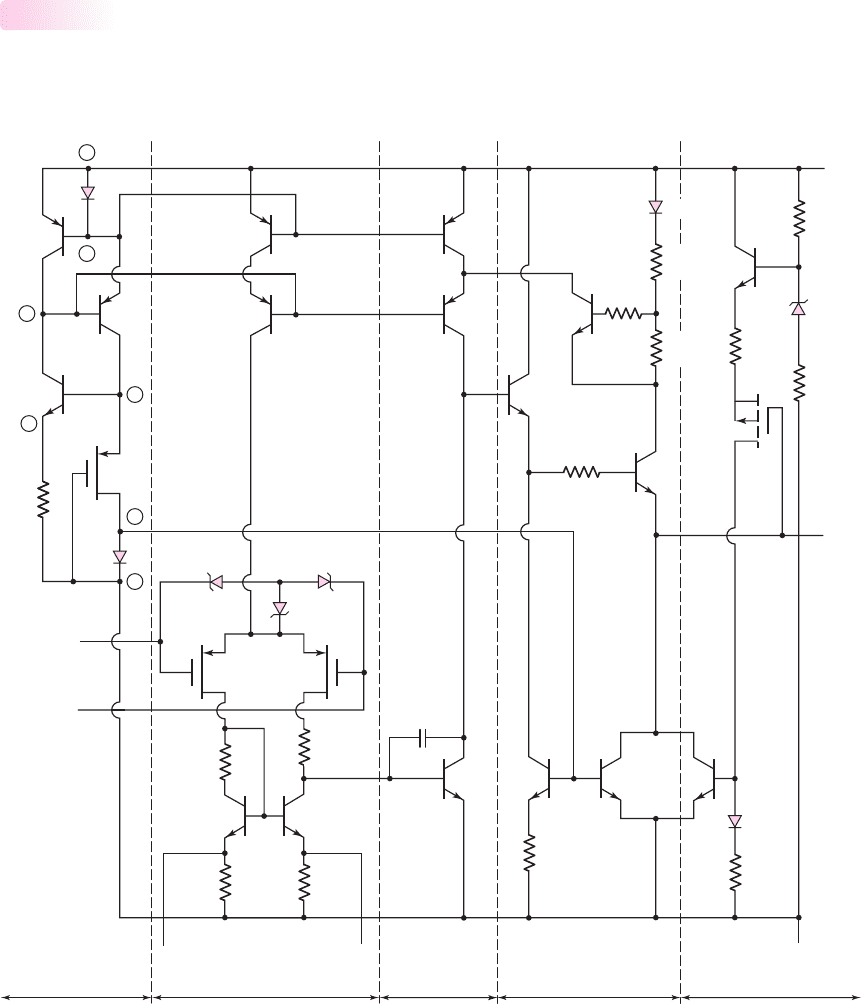
CA3140 BiCMOS Circuit Description
Figure 13.21 shows the basic equivalent circuit of the CA3140 op-amp. Like the 741,
this op-amp consists of three basic stages: the input differential stage, the gain stage, and
13.4.2
Chapter 13 Operational Amplifier Circuits 983
R
7
=
30 Ω
Q
15
Q
16
Q
18
Q
20
Q
19
Q
4
Q
17
D
5
D
4
D
3
D
2
D
1
D
7
D
6
D
8
Q
1
Q
6
Q
7
M
21
M
9
M
10
Q
3
Q
5
Q
2
Q
14
Q
13
Q
12
Q
11
R
6
=
50 Ω
R
5
=
500 Ω
R
3
=
500 Ω
R
2
=
500 Ω
R
4
=
500 Ω
C
1
=
12 pF
R
8
=
1 kΩ
R
12
=
12 kΩ
R
13
=
15 kΩ
R
10
=
1 kΩ
R
14
=
20 kΩ
R
1
=
8 kΩ
–
+
1
3
4
6
5
7
2
V
–
V
+
R
9
=
50 Ω
R
11
=
20 Ω
M
8
Inverting
input
Offset null
Noninverting
input
Output
Bias circuit Input stage Second stage Output stage
Dynamic
current sink
Figure 13.21 CA3140 BiCMOS op-amp equivalent circuit
nea80644_ch13_947-1008.qxd 6/23/09 1:59 PM Page 983 pmath DATA-DISK:Desktop Folder:23/06/09:MHDQ134-13:

the output stage. Also shown in the figure are: the bias circuit, which establishes the dc
bias currents in the op-amp; and a section referred to as a dynamic current sink, which
will be explained later. Typical supply voltages are
V
+
= 15 V
and
V
−
=−15 V
.
Input Diff-Amp
The input differential pair consists of p-channel transistors M
9
and M
10
, and transis-
tors Q
11
and Q
12
form the active load for the diff-amp. A single-sided output at the
collector of Q
12
is the input signal to the following gain stage. Two offset null termi-
nals are also shown, and will be discussed in the next chapter.
MOS transistors are very susceptible to damage from electrostatic charge. For
example, electrostatic voltage can be inadvertently induced on the gate of a MOSFET
during routine handling. These voltages may be great enough to induce breakdown in
the gate oxide, destroying the device. Therefore, input protection against electrostatic
damage is provided by the Zener diodes D
3
, D
4
, and D
5
. If the gate voltage becomes
large enough, these diodes will provide a discharge path for the electrostatic charge,
thus protecting the gate oxide from breakdown.
The dc current biasing is initiated in the bias circuit. The elements labeled D
1
and D
2
are diode-connected transistors. Transistor Q
1
and diode D
1
are matched,
which forces the currents in the two branches of the bias circuit to be equal. The cur-
rent is determined from Q
7
, R
1
, and M
8
. The combination of Q
6
and Q
7
makes the
bias current essentially independent of the power supply voltages.
Gain Stage: The second stage consists of Q
13
connected in a common-emitter
configuration. The cascode configuration of transistors Q
3
and Q
4
provides the bias
current for Q
13
, in addition to acting as the active load. Since Q
3
and Q
4
are connected
in a cascode configuration, the resistance looking into the collector of Q
4
is very high.
Output Stage: The basic output stage consists of the npn transistors Q
17
and Q
18
.
During the positive portion of the output voltage cycle, Q
18
acts as an emitter fol-
lower, supplying a load current. During the negative portion of the output voltage
cycle, Q
16
sinks current from the load. As the output voltage decreases, the source-
to-gate voltage on the p-channel M
21
MOSFET increases, producing a larger current
in D
6
and R
7
so that the base voltage on Q
16
increases. The increase B–E voltage of
Q
16
allows increased load current sinking. Short-circuit protection is provided by the
combination of R
11
and Q
19
. If a sufficiently large voltage is developed across R
11
,
Q
19
turns on and shunts excess base current away from Q
17
.
An abbreviated data sheet for the CA3140 op-amp is in Table 13.2. As before,
we will compare the results of our analysis to the values listed in the table.
984 Part 2 Analog Electronics
Table 13.2 CA3140 BiCMOS data
Parameter Minimum Typical Maximum Units
Input bias current 10 50 pA
Open-loop gain 20,000 100,000 V/V
Unity-gain frequency 4.5 MHz
CA3140 DC Analysis
In this section, we will determine the dc bias currents in the CA3l40 op-amp. As pre-
viously stated, we will concentrate on the features that are unique to the CA3140
compared to the 741.
13.4.3
nea80644_ch13_947-1008.qxd 6/23/09 1:59 PM Page 984 pmath DATA-DISK:Desktop Folder:23/06/09:MHDQ134-13:
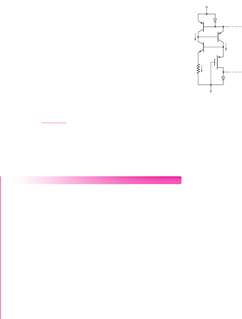
The basic bias circuit is shown in Figure l3.22. The current mirror consisting of
Q
1
and D
1
ensures that the two branch currents I
1
and I
2
are equal, since Q
1
and D
1
are matched. The p-channel MOSFET M
8
is to operate in the saturation region, so
that we must have
V
SD
> V
SG
−
|
V
TP
|
(13.50)
From the figure, we see that
V
SG
= V
SD
+ V
D
(13.51)
or
V
SD
= V
SG
− V
D
(13.52)
Combining Equations (13.52) and (13.50) yields
V
SG
− V
D
> V
SG
−|V
TP
|
(13.53)
which implies that
|V
TP
| > V
D
. In other words, for M
8
to remain biased in the saturation
region, the magnitude of the threshold voltage must be greater than the diode voltage.
From the left branch of the bias circuit, we see that the current can be written
I
2
∼
=
I
R1
=
V
SG
− V
BE7
R
1
(13.54)
and from the right branch, we have
I
1
= K
p
(V
SG
−|V
TP
|)
2
(13.55)
Since
I
1
= I
2
, a simultaneous solution of Equations (13.54) and (13.55) determines
the currents and voltages in this bias circuit.
EXAMPLE 13.12
Objective: Determine the currents and voltages in the bias circuit of the
CA3140 op-amp.
Consider the bias circuit in Figure 13.22, with parameters:
V
+
= 15 V
,
V
−
=
−15 V
, and
R
1
= 8k
. Assume transistor parameters of
V
BE
(npn) = V
EB
(pnp) =
0.6V
for the bipolars, and
K
p
= 0.2mA/V
2
and
|V
TP
|=1.4V
for the MOSFET M
8
.
Solution: Set
I
1
= I
2
. Then, from Equations (13.54) and (13.55), we find
V
SG
= 2.49 V and I
1
= I
2
= 0.236 mA
The voltage at the collector of Q
6
is
V
C6
= V
SG8
+ V
−
= 2.49 −15 =−12.5V
and the voltage at the collector of Q
7
is
V
C7
= V
+
− V
EB1
− V
EB6
= 15 −0.6 −0.6 = 13.8V
Therefore, the collector–base junctions of both Q
6
and Q
7
are reverse biased by
13.8 − (−12.5) = 26.3V
, and both Q
6
and Q
7
are biased in the active region.
Comment: The nominal bias current listed in Table 13.2 is 200
μ
A, which correlates
well with our calculated value of 236
μ
A. As long as the B–C junctions of Q
6
and Q
7
remain reverse biased, the bias currents remain constant. This means that the bias
current is independent of
V
+
and
V
−
over a wide range of voltages.
Chapter 13 Operational Amplifier Circuits 985
Q
7
I
2
R
1
=
8 kΩ
I
1
I
R1
M
8
D
2
D
1
Q
1
V
+
V
–
Q
6
+
–
V
D
+
+
–
–
V
SD
V
SG
Figure 13.22 Bias circuit,
CA3140 BiCMOS op-amp
nea80644_ch13_947-1008.qxd 6/23/09 1:59 PM Page 985 pmath DATA-DISK:Desktop Folder:23/06/09:MHDQ134-13:

The PSpice analysis, using
I
S
= 2 ×10
−15
A
for the BJTs shows that the cur-
rents in the two branches of the current source are essentially
220 μA
. This compares
very favorably with the
236 μA
obtained by the hand analysis.
EXERCISE PROBLEM
Ex 13.12: (a) Assume the bias circuit of the CA3140 op-amp circuit shown in
Figure 13.22 has supply voltages of
V
+
= 5
V and
V
−
=−5
V. Let
R
1
= 10
k
.
The transistor parameters are
V
TP
=−0.8
V and
K
p
= 0.15
mA/V
2
for
M
8
; and
V
BE7
(on) = V
EB6
= 0.6
V for the bipolars. Find the currents
I
1
and
I
2
; and the
voltages
V
SG8
,
V
C7
,
V
C6
,
V
CB7
, and
V
BC6
. (b) Using the results of part (a),
determine the minimum supply voltages that will still maintain the bipolar tran-
sistors biased in the forward active region. Assume
V
+
=−V
−
. (Ans. (a)
I
1
=
I
2
= 0.1028
mA,
V
SG8
= 1.628
V,
V
C7
= 3.8
V,
V
C6
=−3.37
V,
V
CB7
= V
BC6
=
7.17
V; (b)
V
+
=−V
−
= 1.414
V)
Transistors Q
1
through Q
6
and diode D
1
in Figure 13.21 are all matched, which
means that
I
C5
= I
C4
∼
=
200 μA
. The current in D
2
establishes the diode voltage that
also biases Q
14
and Q
15
. The nominal value of I
C18
is 2 mA.
CA3140 Small-Signal Analysis
We analyze the small-signal voltage gain of the CA3140 op-amp by dividing the con-
figuration into its basic circuits and using results previously obtained.
Input Stage
From the results in Chapter 11, the small-signal differential voltage gain can be written
A
d
=
2K
p
I
Q5
(r
o10
R
act1
R
i2
)
(13.56)
where I
Q5
is the bias current supplied by Q
2
and Q
5
. Resistance r
o10
is the output
resistance looking into the drain of M
10
, R
act1
is the effective resistance of the active
load, and R
i2
is the input resistance of the gain stage.
EXAMPLE 13.13
Objective: Calculate the small-signal differential voltage gain of the CA3140 op-
amp input stage. Assume a bias current of
I
Q
= 0.2
mA.
Assume a conduction parameter value of
K
p
= 0.6 mA/V
2
for M
10
, an npn
bipolar current gain of
β
n
= 200
, and a bipolar Early voltage of
V
A
= 50
V.
Solution: The input resistance to the gain stage is
R
i2
= r
π13
; therefore,
R
i2
= r
π13
=
β
n
V
T
I
C13
=
(200)(0.026)
0.20
= 26 k
Resistances r
o10
and R
act1
are normally in the hundreds of kilohms or megohm range,
so the small value of R
i2
dominates the parallel resistance value in the gain expres-
sion. We then have
A
d
∼
=
2K
p
I
Q5
(R
i2
) =
2(0.6)(0.2)(26) = 12.7
Comment: The low input resistance of the gain stage severely loads the input stage,
which in turn results in a relatively low voltage gain for the input stage.
13.4.4
986 Part 2 Analog Electronics
nea80644_ch13_947-1008.qxd 6/23/09 1:59 PM Page 986 pmath DATA-DISK:Desktop Folder:23/06/09:MHDQ134-13:

EXERCISE PROBLEM
Ex 13.13: Repeat Example 13.13 for the case when
K
p
= 1
mA/V
2
for M
10
and
when the Early voltage of a bipolar transistor is
V
A
= 120
V. All other circuit and
transistor parameters are the same as given in Example 13.13. (Ans.
A
d
= 16.4
)
Gain Stage
The magnitude of the small-signal voltage gain for the second stage is
|A
v2
|=g
m13
(r
o13
R
o4
R
i3
)
(13.57)
where R
i3
is the input resistance of the output stage and R
o4
is the output resistance of
the cascode configuration of Q
3
and Q
4
. Transistor Q
17
, which is the input transistor
of the output stage, is connected as an emitter follower, which means that R
i3
is typ-
ically in the megohm range. Similarly, the output resistance R
o4
of the cascode con-
figuration is typically in the megohm range.
The voltage gain of the second stage is then approximately
|A
v2
|
∼
=
g
m13
r
o13
(13.58)
EXAMPLE 13.14
Objective: Calculate the small-signal voltage gain of the second stage of the
CA3140 op-amp.
Assume an Early voltage of
V
A
= 50
V for Q
13
.
Solution: The transconductance is
g
m13
=
I
C13
V
T
=
0.20
0.026
= 7.69 mA/V
and the output resistance is
r
o13
=
V
A
I
C13
=
50
0.20
= 250 k
The voltage gain is therefore
|A
v2
|=g
m13
r
o13
= (7.69)(250) = 1923
Comment: The second stage of the CA3l40 operational amplifier provides the
majority of the voltage gain.
EXERCISE PROBLEM
*Ex 13.14: Assume the gain stage of the CA3140 op-amp is modified to include
an emitter resistor, as shown in Figure 13.23. Let
λ = 0.02 V
−1
for M
10
. Assume
all other transistor parameters are the same as those in Example 13.13. If the tran-
sistor bias currents in M
10
and Q
12
are
100 μA
and the current in Q
13
is
200 μA
,
determine the new value of the small-signal differential voltage gain of the input
stage. (Ans. 69.1)
Chapter 13 Operational Amplifier Circuits 987
R
E13
= 1 kΩ
C
1
= 12 pF
V
–
Q
13
Figure 13.23 Figure for
Exercise Ex 13.14
nea80644_ch13_947-1008.qxd 6/23/09 1:59 PM Page 987 pmath DATA-DISK:Desktop Folder:23/06/09:MHDQ134-13: