Neamen D. Microelectronics: Circuit Analysis and Design
Подождите немного. Документ загружается.

0.01 V
−1
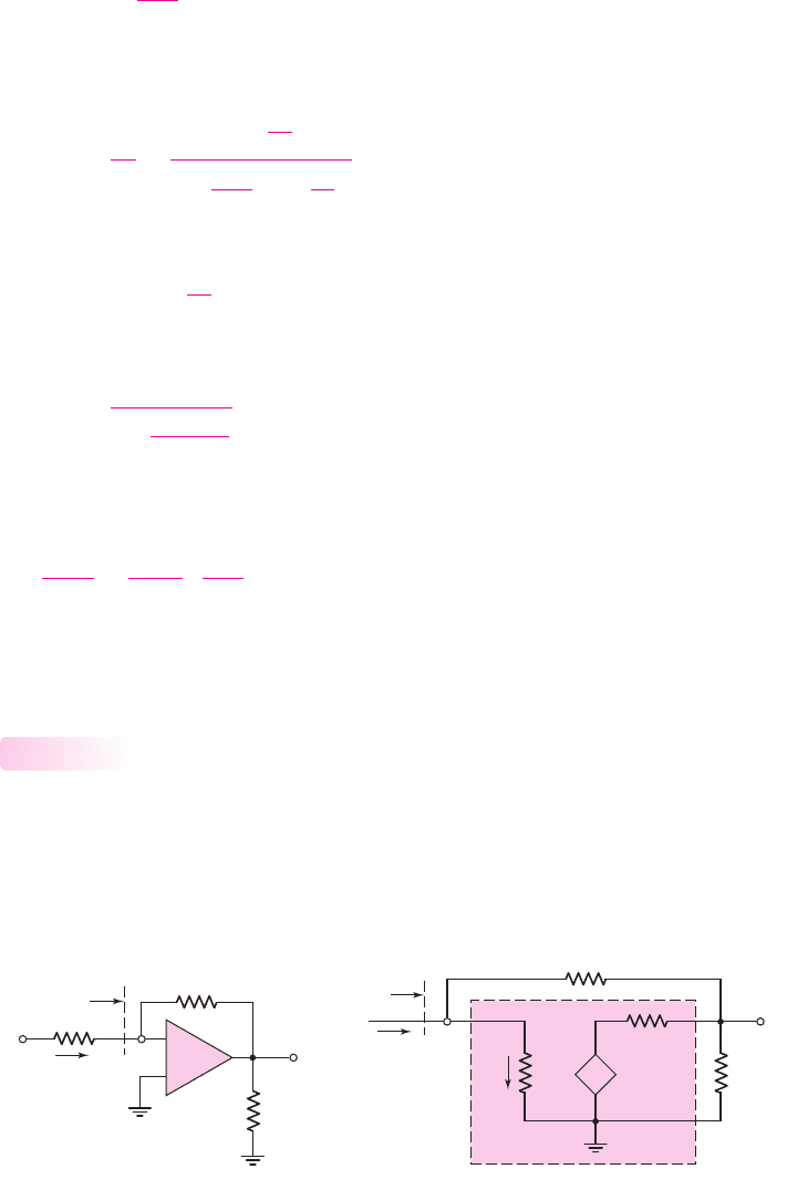
for all transistors. (a) Determine the overall low-frequency dif-
ferential voltage gain. Compare these results with those in Example 13.9.
(b) If the compensation capacitor is
C
1
= 12
pF, plot the magnitude of the
voltage gain versus frequency. What is the 3 dB frequency?
DESIGN PROBLEMS
*D13.67 Consider the input stage and bias circuit of the 741 op-amp shown in Fig-
ure 13.5. Design a complementary circuit such that the input transistors are
pnp devices, and the bias currents are
I
REF
= 0.4
mA and
I
C10
= 24μ
A
when the circuit is biased at
±5
V.
*D13.68 Redesign the CMOS op-amp in Figure 13.14 to provide a minimum over-
all voltage gain of at least 50,000. The bias voltages are
V
+
= 10
V and
V
−
=−10 V
. The threshold voltage is
|V
T
|=1V
for all transistors, and
λ = 0.01 V
−1
for all transistors. Design reasonable width-to-length ratios
and bias currents.
*D13.69 Consider the CMOS op-amp in Figure 13.14. Design a complementary
CMOS circuit in which each element is replaced by its complement. The
bias voltages are
±5
V. The threshold voltage is
|V
T
|=0.7V
for all tran-
sistors, and
λ = 0.01 V
−1
for all transistors. Design reasonable width-to-
length ratios and bias currents to provide a minimum overall voltage gain
of at least 20,000.
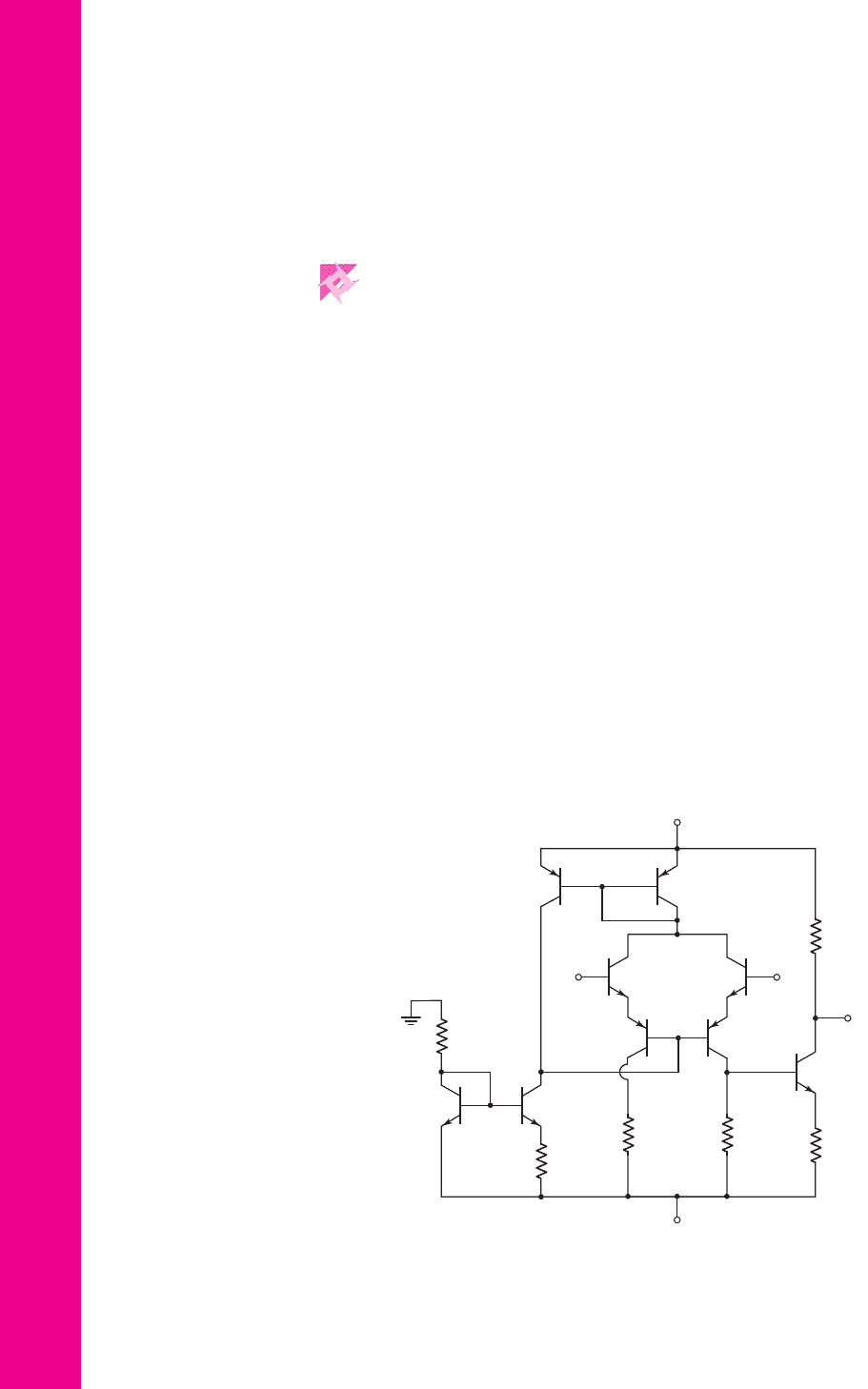
*D13.70 Consider the bipolar op-amp circuit in Figure P13.70. Design the circuit
such that the differential gain is at least 800, and the output voltage is zero
when the input voltages are zero. The transistor current gains are 120 for
all transistors, and the base–emitter voltages are 0.6 V, where appropriate.
1008 Part 2 Analog Electronics
R
3
R
5
R
4
R
2
R
1
V
–
= –15 V
V
+
= 15 V
Q
A
Q
B
Q
4
Q
3
Q
2
Q
D
Q
C
Q
1
Q
5
R
REF
v
–
v
+
v
o
Figure P13.70
nea80644_ch13_947-1008.qxd 6/23/09 1:59 PM Page 1008 pmath DATA-DISK:Desktop Folder:23/06/09:MHDQ134-13:
[Note: Each design should be correlated with a computer analysis.]

1009
Chapter
Nonideal Effects in
Operational Amplifier
Circuits
14
14
1009
Chapter 9 introduced the ideal operational amplifier and covered a few of its many
applications. In the previous chapter, we analyzed actual operational amplifier cir-
cuits, including the classic 741 op-amp. From these discussions, we can identify
sources of nonideal properties in actual op-amps. In particular, we consider the
effects of a finite open-loop gain, reconsider the frequency response, consider the source
and effects of offset voltage, and consider the source and effects of input bias currents.
Although nonideal effects could have been introduced in Chapter 9, that discus-
sion would have been less meaningful since the source of any nonideal effect would
not have been completely understood at that time. In particular, the reason for a very
low dominant-pole frequency in the basic amplifier would have been a mystery.
Therefore, the discussion of nonideal effects in op-amp circuits has been postponed
until now.
PREVIEW
In this chapter, we will:
• Define and discuss various practical op-amp parameters.
• Analyze the effect of finite open-loop gain.
• Analyze the open-loop and closed-loop frequency response.
• Define and analyze sources and effects of offset voltage.
• Define and analyze effects of input bias currents.
• Discuss and analyze additional nonideal properties, such as temperature and
common-mode rejection effects.
• As an application, design an offset voltage compensation network for a CMOS
diff-amp.
nea80644_ch14_1009-1060.qxd 07/12/2009 3:44 Page 1009 pinnacle MHDQ-New:MHDQ134:MHDQ134-14:

1010 Part 2 Analog Electronics
14.1 PRACTICAL OP-AMP PARAMETERS
Objective: • Define and discuss various practical op-amp parameters.
In ideal op-amps, we assume, for example, that the differential voltage gain is infinite,
the input resistance is infinite, and the output resistance is zero. In practical op-amp
circuits, these ideal parameter values are not realized. In this section, we define some of
the practical op-amp parameters that will be considered in detail throughout the chapter.
We will discuss and analyze the effect of these nonideal parameters in op-amp circuits.
Practical Op-Amp Parameter Definitions
Input voltage limits. Two input voltage limitations must be considered—a dc input
voltage limit and a differential signal input voltage. All transistors in the input diff-amp
stage must be properly biased, so there is a limit in the range of common-mode input
voltage that can be applied and still maintain the proper transistor biasing. The maxi-
mum differential input signal voltage that can be applied and still maintain linear cir-
cuit operation is limited primarily by the maximum allowed output signal voltage.
Output voltage limits. The output voltage of the op-amp can never exceed the
limits of the dc supply voltages. In practice, the difference between the bias voltage
and the maximum output voltage depends on the design of the output stage. In older
designs, this difference was on the order of 1 to 2 volts. In newer designs, this differ-
ence can be on the order of millivolts. If
V
out
= A
v
· V
in
(where
A
v
is the overall volt-
age gain) is greater than the bias voltage, then the output voltage would saturate and
would no longer be a linear function of the input voltage.
Output current limitation. The maximum current out of or into the op-amp is
determined by the current ratings of the output transistors. Practical op-amp circuits
cannot source or sink an infinite amount of current.
Finite open-loop voltage gain. The open-loop gain of the ideal op-amp is as-
sumed to be infinite. In practice, the open-loop gain of any op-amp circuit is always
finite. This nonideal parameter value will affect circuit performance.
Input resistance. The input resistance R
i
is the small-signal resistance between
the inverting and noninverting terminals when a differential voltage is applied. Ide-
ally, this parameter is infinite, but, especially for BJT circuits, this parameter is finite.
Output resistance. The output resistance is the Thevenin equivalent small-signal
resistance looking back into the output terminal of the op-amp measured with respect
to ground. The ideal output resistance is zero, which means there is no loading effect
at the output. In practice, this value is not zero.
Finite bandwidth. In the ideal op-amp, the bandwidth is infinite. In practical
op-amps, the bandwidth is finite because of capacitances within the op-amp circuit.
Slew rate. The slew rate is defined as the maximum rate of change in output volt-
age per unit of time. The maximum rate at which the output voltage can change is
also a function of capacitances within the op-amp circuit.
Input offset voltage. In an ideal op-amp, the output voltage is zero for zero dif-
ferential input signal voltage. However, mismatches between input devices, for
example, may create an output voltage with zero input. The input offset voltage is the
applied differential input voltage required to induce a zero output voltage.
14.1.1
nea80644_ch14_1009-1060.qxd 07/12/2009 3:44 Page 1010 pinnacle MHDQ-New:MHDQ134:MHDQ134-14:

Input bias currents. In an ideal op-amp, the input current to the op-amp circuit
is assumed to be zero. However, in practical op-amps, especially with BJT input
devices, the input bias currents are not zero.
The cause of these nonideal op-amp parameters will be discussed in the follow-
ing sections, as well as the effect these nonideal parameters have on op-amp circuit
performance. A few other nonideal parameters will be considered in the last section
of the chapter.
Table 14.1 lists a few of the nonideal parameter values for three of the op-amps
considered in the previous chapter. We will refer to this table as we discuss each of
the nonideal parameters.
Input and Output Voltage Limitations
For linear circuit operation, all BJTs in an op-amp circuit must be biased in the
forward-active region and all MOSFETs must be biased in the saturation region. For
these reasons, there are limitations to the range of input and output voltages in
op-amp circuits.
Figure l4.1(a) shows the simple all-BJT op-amp circuit discussed at the begin-
ning of Chapter 13 and Figure 14.1(b) shows the all-CMOS folded cascode op-amp
circuit discussed in the last chapter. We will use these two circuits to discuss the input
and output voltage limitations.
Input Voltage Limitations
Assume that in the BJT circuit of Figure 14.1(a) we apply a common-mode input
voltage such that
v
cm
= v
1
= v
2
. As
v
cm
increases, the base–collector voltages of
Q
1
and
Q
2
decrease, since the collector voltages are fixed at two base–emitter voltage
drops below
V
+
. If we assume the minimum base–collector voltage is zero so that
the transistor is still biased in the active mode, then the maximum value of
v
cm
is
v
cm
(max) = V
+
−2V
EB
(on)
.
As
v
cm
decreases, the collector–emitter voltage of
Q
3
decreases. If we again as-
sume the minimum base–collector voltage is zero, or the minimum collector–emitter
voltage is
V
BE
(on), then, taking into account the base–emitter voltage of the input
transistors, the minimum value of
v
cm
is
v
cm
(min) = V
−
+2V
BE
(on)
. So the maxi-
mum range of
v
cm
is within approximately 1.4 V of each bias voltage.
14.1.2
Chapter 14 Nonideal Effects in Operational Amplifier Circuits 1011
Table 14.1 Nonideal parameter values for three op-amp circuits
741E CA3140 LH0042C
Typ. Max. Unit Typ. Max. Unit Typ. Max. Unit
Input offset voltage 0.8 3 mV 5 15 mV 6 20 mV
Average input offset voltage drift 15 μV/C10μV/C
Input offset current 3.0 30 nA 0.5 30 pA 2 pA
Average input offset current drift 0.5 nA/C
Input bias current 30 80 nA 10 50 pA 2 10 pA
Slew rate 0.7 V/μs9 V/μs3 V/μs
CMRR 95 dB 90 dB 80 dB
nea80644_ch14_1009-1060.qxd 07/12/2009 3:44 Page 1011 pinnacle MHDQ-New:MHDQ134:MHDQ134-14:
1012 Part 2 Analog Electronics
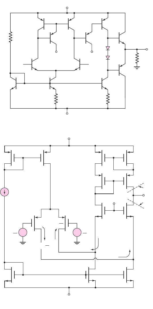
+
–
–
+
v
d
2
v
d
2
R
o6
R
L
R
o8
V
B2
V
+
V
–
V
–
V
–
V
+
V
–
M
1
v
1
v
2
v
2
v
1
M
2
M
3
M
13
M
4
M
6
M
5
M
7
M
9
M
11
I
REF
M
12
M
10
R
3
Q
12
Q
11
Q
8
Q
6
Q
5
Q
7
Q
9
D
2
D
1
Q
10
Q
3
Q
4
Q
2
Q
1
R
2
R
1
M
8
i
i
v
d
2
i = g
m
v
d
2
i = g
m
v
o
v
O
(a)
(b)
Figure 14.1 (a) Simple all-bipolar op-amp circuit; (b) all-CMOS folded cascode op-amp
circuit
nea80644_ch14_1009-1060.qxd 07/12/2009 3:44 Page 1012 pinnacle MHDQ-New:MHDQ134:MHDQ134-14:

The same range of common-mode input voltage can be found for the all-MOSFET
diff-amp in Figure 14.1(b). In this case, all MOSFETs must be biased in the satura-
tion region. We can again define the common-mode input voltage as
v
cm
= v
1
= v
2
.
Now, as
v
cm
increases,
V
SD
of
M
11
decreases. The minimum value of
V
SD
is
V
SD11
(sat) = V
SG11
+ V
TP11
. The maximum value of
v
cm
is then
v
cm
(max) =
V
+
−[V
SG1
+(V
SG11
+ V
TP11
)]
. The gate-to-source voltages can be determined
from the transistor parameters and currents.
As
v
cm
decreases, the source-to-drain voltage of the input transistors decreases.
Assuming that
M
3
and
M
4
are matched to
M
13
, then the drain-to-source voltage of
these transistors is equal to
V
GS13
. The minimum common-mode input voltage is
then
v
cm
(min) = V
−
+[V
GS11
+(V
SG1
+ V
TP1
) − V
SG1
]
. The
V
SG1
terms cancel,
so
v
cm
(min) = V
−
+[V
GS11
+ V
TP1
]
.
Output Voltage Limitations
As the output voltage of the BJT circuit in Figure 14.1(a) increases or decreases, the
collector–emitter voltages of the output transistors change. Again, assuming the min-
imum base–collector voltage is zero for a BJT biased in the forward active region,
then the maximum output voltage is
v
O
(max) = V
+
−[V
EB8
(on) + V
BE11
(on)]
.
The minimum output voltage is similarly found to be
v
O
(min) = V
−
+[V
BE4
(on) +
V
EB12
(on)]
.
For the all-CMOS circuit in Figure 14.1(b), the maximum output voltage
is
v
O
(max) = V
+
−[(V
SG8
+ V
TP8
) + V
SG10
]
. The minimum output voltage is
v
O
(min) = V
−
+[(V
GS6
− V
TN6
) + V
GS13
]
.
Test Your Understanding
TYU 14.1 Using the circuit and transistor parameters of Example 13.11, and assum-
ing threshold voltages of
V
TN
= 0.5
V and
V
TP
=−0.5V
, determine the maximum
range of common-mode input voltage for the all-CMOS folded cascode circuit of
Figure 14.1(b). (Ans.
V
−
−0.184 ≤ v
CM
≤ V
+
−1.13 V
)
TYU 14.2 Using the same circuit and transistor parameters as in Exercise TYU14.1,
calculate the maximum range of output voltage for the all-CMOS folded cascode
circuit of Figure 14.1(b). (Ans.
V
−
+0.54 V ≤ v
O
≤ V
+
−1.13 V
)
14.2 FINITE OPEN-LOOP GAIN
Objective: • Analyze the effect of finite open-loop gain.
In the ideal op-amp, the open-loop gain is infinite, the input differential resistance is
infinite, and the output resistance is zero. None of these conditions exists in actual
operational amplifiers. In the last chapter, we determined that the open-loop gain and
input differential resistance may be large but finite, and the output resistance may be
small but nonzero. In this section, we will determine the effect of a finite open-loop
gain and input resistance on both the inverting and noninverting amplifier character-
istics. We will then calculate the output resistance.
In this section, we limit our discussion of the finite open-loop gain to low fre-
quency. In the next section, we consider the effect of finite gain as well as the
frequency response of the amplifier.
Chapter 14 Nonideal Effects in Operational Amplifier Circuits 1013
nea80644_ch14_1009-1060.qxd 07/12/2009 3:44 Page 1013 pinnacle MHDQ-New:MHDQ134:MHDQ134-14:
Inverting Amplifier Closed-Loop Gain
The equivalent circuit of the inverting amplifier with a finite open-loop gain is shown
in Figure 14.2. If the open-loop input resistance is assumed to be infinite, then
i
1
= i
2
,or
v
I
−v
1
R
1
=
v
1
−v
O
R
2
(14.1(a))
or
v
I
R
1
= v
1
1
R
1
+
1
R
2
−
v
O
R
2
(14.1(b))
Since
v
2
= 0
, the output voltage is
v
O
=−A
OL
v
1
(14.2)
where
A
OL
is the low-frequency open-loop gain. Solving for
v
1
from Equation (14.2)
and substituting the result into Equation (14.1(b)), we find
v
I
R
1
=−
v
O
A
OL
1
R
1
+
1
R
2
−
v
O
R
2
(14.3)
The closed-loop voltage gain is then
A
CL
=
v
O
v
I
=
−
R
2
R
1
1 +
1
A
OL
1 +
R
2
R
1
(14.4)
EXAMPLE 14.1
Objective: Determine the minimum open-loop voltage gain to achieve a particular
accuracy.
A pressure transducer produces a maximum dc voltage signal of 2 mV and has
an output resistance of
R
S
= 2k
. The maximum dc current from the transducer is
to be limited to 0.2
μ
A. An inverting amplifier is to be used in conjunction with the
transducer to produce an output voltage of
−0.10 V
for a 2 mV transducer signal.
The error in the output voltage cannot be greater than 0.1 percent. Determine the
minimum open-loop gain of the amplifier to meet this specification.
14.2.1
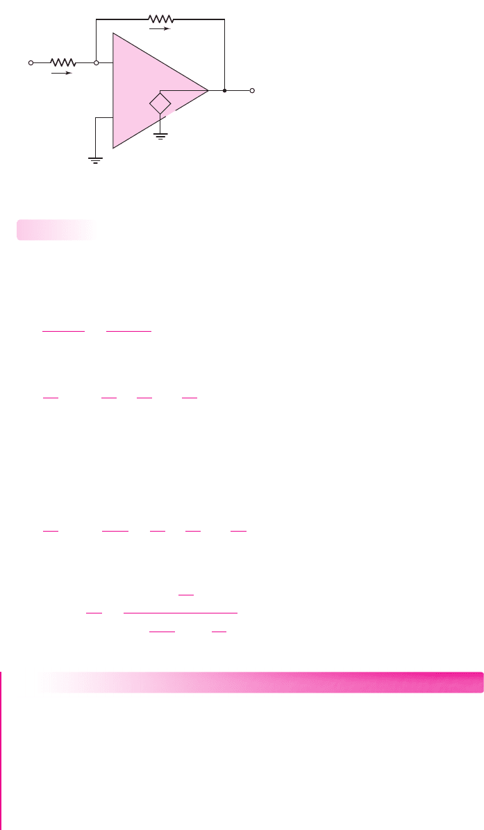
1014 Part 2 Analog Electronics
v
2
R
1
i
1
R
2
v
1
i
2
v
O
v
I
–
+
+
–
A
OL
(v
2
– v
1
)
Figure 14.2 Equivalent circuit, inverting amplifier with finite open-loop gain
nea80644_ch14_1009-1060.qxd 07/12/2009 3:44 Page 1014 pinnacle MHDQ-New:MHDQ134:MHDQ134-14:

Solution: We must first determine the resistor values to be used in the inverting am-
plifier. The source resistor is in series with
R
1
, so let
R
1
= R
1
+ R
S
The minimum input resistance is found from the maximum input current as
R
1
(min) =
v
i
i
i
(max)
=
2 × 10
−3
0.2 × 10
−6
= 10 ×10
3
= 10 k
The resistor
R
1
then needs to be
8k
. The closed-loop voltage gain required is
A
CL
=
v
O
v
i
=
−0.10
2 × 10
−3
=−50 =
−R
F
R
1
The required value of the feedback resistor is then
R
F
= 500 k
.
For the voltage gain to be within 0.1 percent, the minimum gain (magnitude) is
49.95. Using Equation (14.4), we can determine the minimum value of the open-loop
gain. We have
A
CL
=
−R
2
R
1
1 +
1
A
OL
1 +
R
2
R
1
=−49.95 =
−50
1 +
1
A
OL
(51)
which yields
A
OL
(min) = 50,949
.
Comment: If the open-loop gain is greater than the value of A
OL
(min) = 50,949,
then the error in the voltage gain will be less than 0.1 percent.
EXERCISE PROBLEM
Ex 14.1: Consider an inverting amplifier in which the op-amp open-loop gain is
A
OL
= 2 ×10
5
and the ideal closed-loop amplifier gain is
A
CL
(
∞
)
=−40
.
(a) Determine the actual closed-loop gain. (b) Repeat part (a) if the open-loop gain is
A
OL
= 5 ×10
4
. (c) What is the percent change between the magnitudes of the actual
gains from part (a) to part (b)? (Ans. (a)
−
39.9918, (b)
−
39.9672, (c)
−
0.0615%)
In the limit as
A
OL
→∞
, the closed-loop gain is equal to the ideal value,
designated
A
CL
(∞)
, which for the inverting amplifier is
A
CL
(∞) =−
R
2
R
1
(14.5)
as previously determined. Equation (14.4) is then
A
CL
=
A
CL
(∞)
1 +
1 − A
CL
(∞)
A
OL
(14.6)
To determine the variation in closed-loop gain with changes in open-loop gain,
we take the derivative of
A
CL
with respect to
A
OL
. We find
dA
CL
dA
OL
=
A
CL
(∞)(1 − A
CL
(∞))
[A
OL
+(1 − A
CL
(∞))]
2
(14.7)
Chapter 14 Nonideal Effects in Operational Amplifier Circuits 1015
nea80644_ch14_1009-1060.qxd 07/12/2009 3:44 Page 1015 pinnacle MHDQ-New:MHDQ134:MHDQ134-14:
which can be rearranged in the form
dA
CL
A
CL
=
dA
OL
A
OL
1 − A
CL
(∞)
A
OL
1 +
1 − A
CL
(∞)
A
OL
(14.8)
Normally,
A
CL
(∞)||A
OL
|
and Equation (14.8) is approximately
dA
CL
A
CL
∼
=
dA
OL
A
OL
1 − A
CL
(∞)
A
OL
(14.9)
Equation (14.9) relates the percent change in the closed-loop gain of the invert-
ing amplifier as the result of a change in open-loop gain. Open-loop gain variations
occur when individual transistor parameters change from one circuit to another or
with temperature.
From Equation (14.9), we see that changes in closed-loop gain become smaller
as the open-loop gain becomes larger.
Noninverting Amplifier Closed-Loop Gain
Figure 14.3 shows the equivalent circuit of the noninverting amplifier with a finite
open-loop gain. Again, the open-loop input differential resistance is assumed to be
infinite. The analysis proceeds in much the same way as in the previous section.
We have
i
1
= i
2
, and
−
v
1
R
1
=
v
1
−v
O
R
2
(14.10(a))
or
v
O
R
2
= v
1
1
R
1
+
1
R
2
(14.10(b))
The output voltage is
v
O
= A
OL
(v
2
−v
1
)
(14.11)
14.2.2
1016 Part 2 Analog Electronics
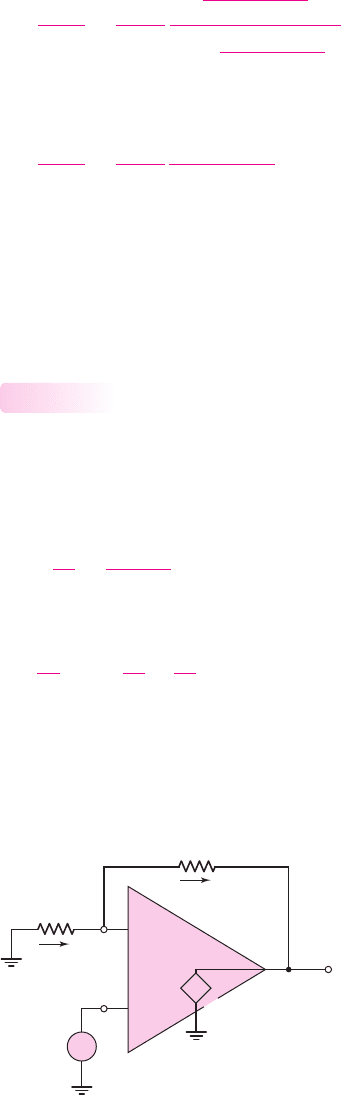
v
2
R
1
i
1
R
2
v
1
i
2
v
O
v
I
–
+
+
–
A
OL
(v
2
– v
1
)
+
–
Figure 14.3 Equivalent circuit, noninverting amplifier with finite open-loop gain
nea80644_ch14_1009-1060.qxd 07/12/2009 3:44 Page 1016 pinnacle MHDQ-New:MHDQ134:MHDQ134-14:
Since
v
2
= v
I
, voltage
v
1
can be written
v
1
= v
I
−
v
O
A
OL
(14.12)
Combining Equations (14.12) and (14.10(b)) and rearranging terms, we have an ex-
pression for the closed-loop voltage gain:
A
CL
=
v
O
v
I
=
1 +
R
2
R
1
1 +
1
A
OL
1 +
R
2
R
1
(14.13)
In the limit as
A
OL
→∞
, the ideal closed-loop gain is
A
CL
(∞) = 1 +
R
2
R
1
(14.14)
and Equation (14.13) becomes
A
CL
=
A
CL
(∞)
1 +
A
CL
(∞)
A
OL
(14.15)
Taking the derivative of the closed-loop gain with respect to the open-loop gain
and rearranging terms, we obtain
dA
CL
A
CL
=
dA
OL
A
OL
A
CL
A
OL
(14.16)
Equation (14.16) yields the fractional change in the closed-loop gain of the non-
inverting amplifier as a result of a change in the open-loop gain. The result for the
noninverting amplifier is very similar to that for the inverting amplifier.
Inverting Amplifier Closed-Loop Input Resistance
The closed-loop input resistance
R
if
of the inverting amplifier is defined in Fig-
ure 14.4(a), and it includes the effect of feedback. The equivalent circuit, including a
finite open-loop gain
A
OL
, finite open-loop input differential resistance
R
i
, and
nonzero output resistance
R
o
, is shown in Figure 14.4(b).
14.2.3
Chapter 14 Nonideal Effects in Operational Amplifier Circuits 1017
R
1
i
1
R
2
v
1
v
O
v
I
R
if
R
L
–
+
R
i
R
i
f
R
o
–A
OL
v
1
R
L
v
O
R
2
i
i
i
1
v
1
(a) (b)
–
+
+
–
Figure 14.4 (a) Inverting amplifier and (b) inverting amplifier equivalent circuit, for
calculating closed-loop input resistance
nea80644_ch14_1009-1060.qxd 07/12/2009 3:44 Page 1017 pinnacle MHDQ-New:MHDQ134:MHDQ134-14: