Neamen D. Microelectronics: Circuit Analysis and Design
Подождите немного. Документ загружается.

Sections 14.4 and 14.5 Offset Voltage and Input Bias Current: Total Effects
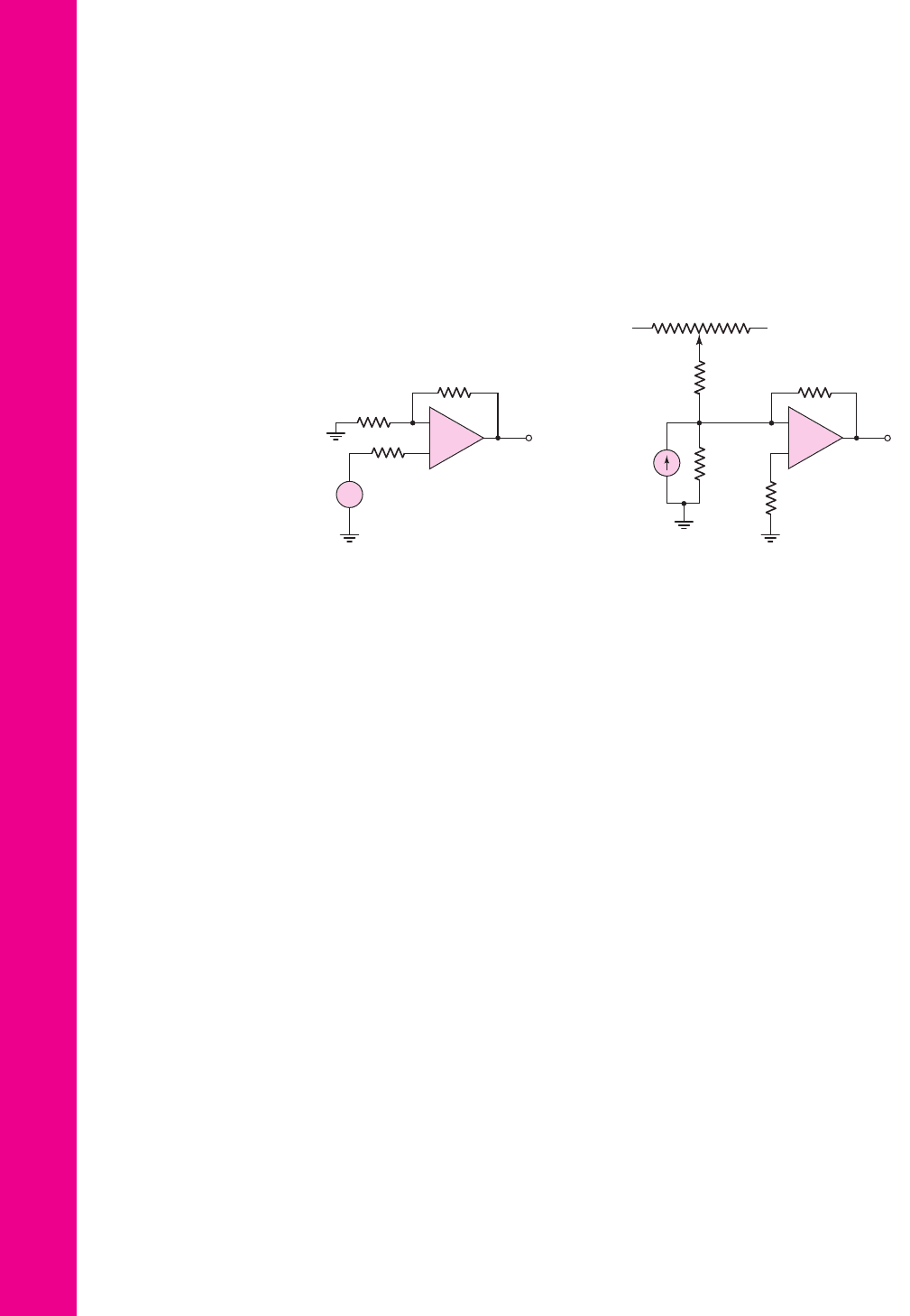
14.51 For the op-amp in Figure P14.51, the input offset voltage is
V
OS
= 3
mV,
the average input bias current is
I
B
= 0.4 μ
A, and the offset bias current is
I
OS
= 0.06 μ
A. (a) Determine the possible range in output voltage for
v
I
= 0
and
R = 0
. (b) Repeat part (a) for
v
I
= 0
and
R = 9.09
k
.
(c) Repeat part (a) for
v
I
= 0.2
V and
R = 9.09
k
.
1058 Part 2 Analog Electronics
D14.52 Consider the op-amp circuit in Figure P14.52. (a) Find the value of R
2
needed for a
±10
mV offset voltage adjustment. (b) Determine R
1
to mini-
mize bias current effects. (Assume
R
2
R
i
.)
D14.53 For each op-amp in the circuit in Figure P14.38, the offset voltage is
V
OS
= 10
mV and the input bias currents are
I
B1
= I
B2
= 2 μ
A. (a) Find
the worst-case output voltages
v
O1
and
v
O2
for
v
I
= 0
. (b) Design compen-
sation circuits to adjust both v
O1
and v
O2
to zero when
v
I
= 0
.
14.54 The op-amps in the circuit in Figure P14.49 have an offset voltage
V
OS
= 2
mV, an average input bias current of
I
B
= 0.2 μ
A, and an offset
current of
I
OS
= 0.02 μ
A. (a) For
v
I
= 0
and
R
A
= R
B
= 0
, determine the
possible range in output voltages
v
O1
,
v
O2
, and
v
O3
. (b) Repeat part (a) for
R
A
= 8.33
k
and
R
B
= 10
k
.
14.55 Each op-amp in Figure P14.50 has an offset voltage of
V
OS
= 2
mV, an
average input bias current of
I
B
= 500
nA, and an input offset current
of
I
OS
=
100 nA. Determine the worst-case output voltage for each
circuit.
Section 14.6 Additional Nonideal Effects
14.56 For each op-amp in Figure P14.50, the input offset voltage is
V
OS
= 2
mV
at
T = 25
◦
C
and the input offset voltage temperature coefficient is
TCv
OS
= 6.7 μ
V/°C. Find the output voltage v
O
due to the input offset
voltage effects at: (a)
T = 25
◦
C and (b)
T = 50
◦
C.
14.57 The input offset voltage in each op-amp in Figure P14.57 is
V
OS
= 1
mV at
T = 25
◦
C and the input offset voltage coefficient is TCv
OS
= 3.3
μ
V/
◦
C.
Find the worst-case output voltages
v
O1
and
v
O2
at: (a)
T = 25
◦
C and
(b)
T = 50
◦
C.
10 kΩ
100 kΩ
v
O
v
I
–
+
R
+
–
–
+
Figure P14.51
100 kΩ
+15 V
–
15 V
R
1
R
F
= 10 kΩ
R
i
=
15 kΩ
R
2
v
O
i
I
–
+
–
+
Figure P14.52
nea80644_ch14_1009-1060.qxd 07/12/2009 3:45 Page 1058 pinnacle MHDQ-New:MHDQ134:MHDQ134-14:
14.58 For each op-amp in Figure P14.50, the input bias current is
I
B
= 500
nA
at
T = 25
◦
C, the input offset current is
I
OS
= 200
nA at
T = 25
◦
C, the
input bias current temperature coefficient is 8 nA/
◦
C, and the input offset
current temperature coefficient is 2 nA/
◦
C. (a) Find the output voltage due
to the average input bias currents at
T = 25
◦
C. (b) Find the worst-case out-
put voltage due to the input bias current and input offset current at
T = 25
◦
C. (c) Repeat parts (a) and (b) for
T = 50
◦
C.
14.59 For each op-amp in Figure P14.57, the input bias current is
I
B
= 2 μ
A
at
T = 25
◦
C, the input offset current is
I
OS
= 0.2 μ
A at
T = 25
◦
C, the
input bias current temperature coefficient is 20 nA/
◦
C, and the input offset
current temperature coefficient is 5 nA/
◦
C. (a) Find the worst-case output
voltages
v
O1
and
v
O2
due to the average input bias currents at
T = 25
◦
C.
(b) Find the worst-case output voltages
v
O1
and
v
O2
due to the input bias
currents and input offset current at
T = 25
◦
C. (c) Repeat parts (a) and
(b) for
T = 50
◦
C.
14.60 The op-amp in the difference amplifier configuration in Figure P14.60 is
ideal. (a) If the tolerance of each resistor is
±1.5%
, determine the minimum
value of
CMRR
dB
. (b) Repeat part (a) if the tolerance of each resistor is
±3%
.
14.61 If the tolerance of each resistor in the difference amplifier in Figure P14.60
is
±x%
, what is the maximum value of
x
if the minimum
CMRR
dB
is (a) 50 dB
and (b) 75 dB.
Chapter 14 Nonideal Effects in Operational Amplifier Circuits 1059
10 kΩ
50 kΩ
20 kΩ
50 kΩ
60 kΩ
v
O2
v
O1
v
I
–
+
–
+
Figure P14.57
v
O
v
I1
10 kΩ
10 kΩ
50 kΩ
50 kΩ
v
I2
–
+
Figure P14.60
COMPUTER SIMULATION PROBLEMS
14.62 Consider an inverting amplifier such as shown in Figure 14.2. Bias a stan-
dard op-amp at
±5
V, and let
R
2
= 100
k
and
R
1
= 10
k
. Using a com-
puter simulation, plot
v
O
versus
v
I
over the range
−0.7 ≤ v
I
≤ 0.7
V. What
is the output saturation voltage?
nea80644_ch14_1009-1060.qxd 07/12/2009 3:45 Page 1059 pinnacle MHDQ-New:MHDQ134:MHDQ134-14:

14.63 Consider the simplified op-amp shown in Figure 14.11. Use standard tran-
sistors and take the output at the collector of
Q
6
. Assume the bias current for
Q
1
and
Q
2
is
I
Q
= 19 μA
and the bias current for
Q
5
and
Q
6
is
I
Q
= 0.15
mA.
Let
C
1
= 30
pF. (a) Using a computer simulation, determine the slew rate of
the amplifier. (b) Using a computer simulation, determine the small-signal
bandwidth for (i)
v
d
= 1 μ
V and (ii)
v
d
= 5 μ
V. Use an appropriate load.
14.64 The equivalent circuit of the all-CMOS MC14573 op-amp was given in
Figure 13.14. Using a computer simulation, determine the slew rate of the
op-amp assuming
C
1
= 12
pF. Use standard transistors.
14.65 A basic bipolar input diff-amp stage is shown in Figure 14.22. Use standard
transistors and other appropriate circuit parameters. Let
v
1
= v
2
= 0
.
(a) Plot
i
C1
and
i
C2
as a function of the wiper arm position
x
. (b) Plot the
collector voltage of
Q
4
as a function of wiper arm position
x
.
DESIGN PROBLEMS
[Note: Each design should be verified with a computer analysis.]
*D14.66An amplifier system, using op-amps, is to be designed to provide a low-
frequency voltage gain of 50 and a bandwidth of 20 kHz. The only available
op-amps have a low-frequency open-loop voltage gain of
3 × 10
4
and a
bandwidth of 10 Hz. Design an appropriate system.
*D14.67Consider the simplified op-amp in Figure 14.11. Neglect the emitter-fol-
lower output stage. Assume bias voltages of
V
+
= 3
V and
V
−
=−3V
. Let
the bias current for
Q
5
and
Q
6
be
I
Q
= 0.1
mA. The total power dissipated
in the circuit is to be limited to 0.65 mW. Design the circuit such that the
slew rate is
2
V/
μ
s. Determine
I
Q
for
Q
1
and
Q
2
, and find the appropriate
value for
C
1
.
*D14.68Consider the op-amp circuit shown in Figure P14.12. Each op-amp has an
offset voltage of
V
OS
= 2
mV. Design an offset voltage compensation
circuit. Assume bias voltages are limited to
±5
V.
*D14.69Consider the op-amp circuit shown in Figure P14.12. Each op-amp has an
average input bias current of
I
B
= 1 μ
A and the offset bias current is
I
OS
= 0.1 μ
A. Design an optimum bias-current compensation circuit. What
is the possible range of output voltage
v
O2
for
v
I
= 0
?
1060 Part 2 Analog Electronics
nea80644_ch14_1009-1060.qxd 07/12/2009 3:45 Page 1060 pinnacle MHDQ-New:MHDQ134:MHDQ134-14:

Chapter
Applications and Design
of Integrated Circuits
15
15
1061
In Chapter 9, we introduced the ideal operational amplifier and analyzed and designed
basic op-amp circuits. In this chapter, we consider additional applications and designs
of op-amp and comparator circuits that may be fabricated as integrated circuits.
A comparator is essentially an op-amp operated in an open-loop configuration with
either a high or low saturated output signal.
Circuits to be considered include active filters, oscillators, Schmitt trigger cir-
cuits, integrated circuit power amplifiers, and voltage regulators.
A general goal of this chapter is to increase our skill at designing electronic
circuits to meet particular specifications and to perform particular functions.
PREVIEW
In this chapter, we will:
• Analyze and design active filters that transmit desired frequency components
of an input signal and attenuate undesired frequency components.
• Analyze and design oscillators that provide sinusoidal signals at specified
frequencies.
• Analyze and design various Schmitt trigger circuits.
• Analyze and design multivibrator circuits that provide signals with particular
waveforms.
• Analyze and design IC power amplifiers that usually consist of high-gain
small-signal amplifiers in cascade with an output stage.
• Analyze and design voltage regulators that establish a relatively constant dc
voltage generated from an ac signal source.
• As an application, design an active bandpass filter to meet a set of specifications.
nea80644_ch15_1061-1140.qxd 07/12/2009 3:58 Page 1061 pinnacle MHDQ-New:MHDQ134:MHDQ134-15:

1062 Part 2 Analog Electronics
15.1 ACTIVE FILTERS
Objective: • Analyze and design active filters that transmit desired
frequency components of an input signal and attenuate undesired fre-
quency components.
An important application of an op-amp is the active filter. The word filter refers to
the process of removing undesired portions of the frequency spectrum. The word
active implies the use of one or more active devices, usually an operational amplifier,
in the filter circuit. As an example of the application of op-amps in the area of active
filters, we will discuss the Butterworth filter. There are many types or classifications
of filters. However, the objective here is to concentrate mainly on a single type
(Butterworth) in order to demonstrate the use of op-amps in filter design. Additional
types of filters are discussed in other references.
Two advantages of active filters over passive filters are:
1. The maximum gain or the maximum value of the transfer function may be
greater than unity.
2. The loading effect is minimal, which means that the output response of the filter
is essentially independent of the load driven by the filter.
Active Network Design
From our discussions of frequency response in Chapter 7, we know that RC networks
form filters. Figure 15.1(a) is a simple example of a coupling-capacitor circuit. The
voltage transfer function for this circuit is
T (s) =
V
o
(s)
V
i
(s)
=
R
R +
1
sC
=
sRC
1 + sRC
(15.1)
The Bode plot of the voltage gain magnitude
|T ( jω)|
is shown in Figure 15.1(b). The
circuit is called a high-pass filter.
Figure 15.2(a) is another example of a simple RC network. Here, the voltage
transfer function is
T (s) =
V
o
(s)
V
i
(s)
=
1
sC
1
sC
+ R
=
1
1 + sRC
(15.2)
15.1.1
(a)
|T( jw)|
f
f
L
0
1
Stopband Passband
(b)
V
i
V
o
C
R
Figure 15.1 (a) Simple high-pass filter and (b) Bode plot of transfer function magnitude
nea80644_ch15_1061-1140.qxd 07/12/2009 3:58 Page 1062 pinnacle MHDQ-New:MHDQ134:MHDQ134-15:
Chapter 15 Applications and Design of Integrated Circuits 1063
(a)
|T( jw)|
f
f
H
0
1
StopbandPassband
(b)
V
i
V
o
R
C
Figure 15.2 (a) Simple low-pass filter and (b) Bode plot of transfer function magnitude
(a)
V
i
V
o
C
R
–
+
(b)
R
V
i
V
o
C
–
+
Figure 15.3 (a) High-pass filter with voltage follower and (b) low-pass filter with voltage
follower
The Bode plot of the voltage gain magnitude
|T ( jω)|
for this circuit is shown in
Figure 15.2(b). This circuit is called a low-pass filter.
Although these circuits both perform a basic filtering function, they may suffer
from loading effects, substantially reducing the maximum gain from the unity value
shown in Figures 15.1(b) and 15.2(b). Also, the cutoff frequencies
f
L
and
f
H
may
change when a load is connected to the output. The loading effect can essentially be
eliminated by using a voltage follower as shown in Figure 15.3. In addition, a nonin-
verting amplifier configuration can be incorporated to increase the gain, as well as
eliminate the loading effects.
These two filter circuits are called one-pole filters; the slope of the voltage gain
magnitude curve outside the passband is 6 dB/octave or 20 dB/decade. This charac-
teristic is called the rolloff. The rolloff becomes sharper or steeper with higher-order
filters and is usually one of the specifications given for active filters.
Two other categories of filters are bandpass and band-reject. The desired ideal
frequency characteristics are shown in Figure 15.4.
(a)
|T( jw )|
f
f
L
f
H
1
(b)
|T( jw )|
f
f
L
f
H
1
Figure 15.4 Ideal frequency characteristics: (a) bandpass filter and (b) band-reject filter
nea80644_ch15_1061-1140.qxd 07/12/2009 3:58 Page 1063 pinnacle MHDQ-New:MHDQ134:MHDQ134-15:
1064 Part 2 Analog Electronics
+
–
V
i
V
a
V
b
V
o
Y
1
Y
2
Y
4
Y
3
–
+
Figure 15.5 General two-pole active filter
General Two-Pole Active Filter
Consider Figure 15.5 with admittances
Y
1
through
Y
4
and an ideal voltage follower.
We will derive the transfer function for the general network and will then apply spe-
cific admittances to obtain particular filter characteristics.
15.1.2
A KCL equation at node
V
a
yields
(V
i
− V
a
)Y
1
= (V
a
− V
b
)Y
2
+(V
a
− V
o
)Y
3
(15.3)
A KCL equation at node
V
b
produces
(V
a
− V
b
)Y
2
= V
b
Y
4
(15.4)
From the voltage follower characteristics, we have
V
b
= V
o
. Therefore, Equa-
tion (15.4) becomes
V
a
= V
b
Y
2
+ Y
4
Y
2
= V
o
Y
2
+ Y
4
Y
2
(15.5)
Substituting Equation (15.5) into (15.3) and again noting that
V
b
= V
o
, we have
V
i
Y
1
+ V
o
(Y
2
+ Y
3
) = V
a
(Y
1
+ Y
2
+ Y
3
)
= V
o
Y
2
+ Y
4
Y
2
(Y
1
+ Y
2
+ Y
3
)
(15.6)
Multiplying Equation (15.6) by
Y
2
and rearranging terms, we get the following
expression for the transfer function:
T (s) =
V
o
(s)
V
i
(s)
=
Y
1
Y
2
Y
1
Y
2
+ Y
4
(Y
1
+ Y
2
+ Y
3
)
(15.7)
To obtain a low-pass filter, both
Y
1
and
Y
2
must be conductances, allowing the
signal to pass into the voltage follower at low frequencies. If element
Y
4
is a capaci-
tor, then the output rolls off at high frequencies.
To produce a two-pole function, element
Y
3
must also be a capacitor. On the
other hand, if elements
Y
1
and
Y
2
are capacitors, then the signal will be blocked at
low frequencies but will be passed into the voltage follower at high frequencies, re-
sulting in a high-pass filter. Therefore, admittances
Y
3
and
Y
4
must both be conduc-
tances to produce a two-pole high-pass transfer function.
nea80644_ch15_1061-1140.qxd 07/12/2009 3:58 Page 1064 pinnacle MHDQ-New:MHDQ134:MHDQ134-15:
Chapter 15 Applications and Design of Integrated Circuits 1065
V
i
V
o
C
3
C
4
R
1
=
1
G
1
R
2
=
1
G
2
–
+
Figure 15.6 General two-pole low-pass filter
Two-Pole Low-Pass Butterworth Filter
To form a low-pass filter, we set
Y
1
= G
1
= 1/R
1
,
Y
2
= G
2
= 1/R
2
,
Y
3
= sC
3
, and
Y
4
= sC
4
, as shown in Figure 15.6. The transfer function, from Equation (15.7),
becomes
T (s) =
V
o
(s)
V
i
(s)
=
G
1
G
2
G
1
G
2
+sC
4
(G
1
+ G
2
+sC
3
)
(15.8)
15.1.3
At zero frequency,
s = jω = 0
and the transfer function is
T (s = 0) =
G
1
G
2
G
1
G
2
= 1
(15.9)
In the high-frequency limit,
s = jω →∞
and the transfer function approaches zero.
This circuit therefore acts as a low-pass filter.
A Butterworth filter is a maximally flat magnitude filter. The transfer func-
tion is designed such that the magnitude of the transfer function is as flat as possible
within the passband of the filter. This objective is achieved by taking the derivatives
of the transfer function with respect to frequency and setting as many as possible
equal to zero at the center of the passband, which is at zero frequency for the low-
pass filter.
Let
G
1
= G
2
≡ G = 1/R
. The transfer function is then
T (s) =
1
R
2
1
R
2
+sC
4
2
R
+sC
3
=
1
1 + sRC
4
(2 + sRC
3
)
(15.10)
We define time constants at
τ
3
= RC
3
and
τ
4
= RC
4
. If we then set
s = jω
,we
obtain
T ( jω) =
1
1 + jωτ
4
(2 + jωτ
3
)
=
1
(1 − ω
2
τ
3
τ
4
) + j(2ωτ
4
)
(15.11)
The magnitude of the transfer function is therefore
|T ( jω)|=[(1 − ω
2
τ
3
τ
4
)
2
+(2ωτ
4
)
2
]
−1/2
(15.12)
nea80644_ch15_1061-1140.qxd 07/12/2009 3:58 Page 1065 pinnacle MHDQ-New:MHDQ134:MHDQ134-15:

1066 Part 2 Analog Electronics
For a maximally flat filter (that is, a filter with a minimum rate of change), which
defines a Butterworth filter, we set
d|T |
dω
ω=0
= 0
(15.13)
Taking the derivative, we find
d|T |
dω
=−
1
2
[(1 − ω
2
τ
3
τ
4
)
2
+(2ωτ
4
)
2
]
−3/2
−4ωτ
3
τ
4
(1 − ω
2
τ
3
τ
4
) + 8ωτ
2
4
(15.14)
Setting the derivative equal to zero at
ω = 0
yields
d|T |
dω
ω=0
=
−4ωτ
3
τ
4
(1 − ω
2
τ
3
τ
4
) + 8ωτ
2
4
= 4ωτ
4
[−τ
3
(1 − ω
2
τ
3
τ
4
) + 2τ
4
]
(15.15)
Equation (15.15) is satisfied when
2τ
4
= τ
3
,or
C
3
= 2C
4
(15.16)
For this condition, the transfer magnitude is, from Equation (15.12),
|T |=
1
[1 + 4(ωτ
4
)
4
]
1/2
(15.17)
The 3 dB, or cutoff, frequency occurs when
|T |=1/
√
2
, or when
4(ω
3dB
τ
4
)
4
= 1
.
We then find that
ω
3dB
= 2π f
3dB
=
1
τ
4
√
2
=
1
√
2RC
4
(15.18)
In general, we can write the cutoff frequency in the form
ω
3dB
=
1
RC
(15.19)
Finally, comparing Equations (15.19), (15.18), and (15.16) yields
C
4
= 0.707C
(15.20(a))
and
C
3
= 1.414C
(15.20(b))
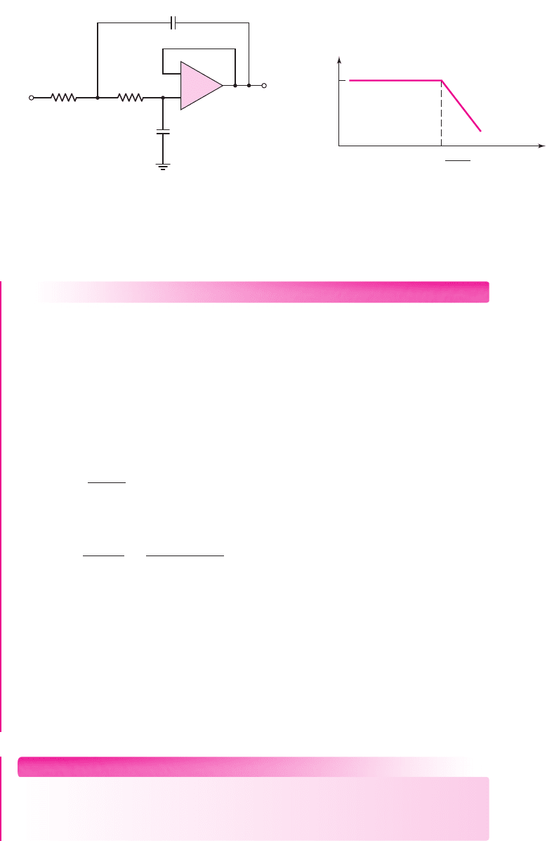
The two-pole low-pass Butterworth filter is shown in Figure 15.7(a). The Bode
plot of the transfer function magnitude is shown in Figure 15.7(b). From Equa-
tion (15.17), the magnitude of the voltage transfer function for the two-pole low-pass
Butterworth filter can be written as
|T |=
1
1 +
f
f
3dB
4
(15.21)
Equation (15.15) shows that the derivative of the voltage transfer function mag-
nitude at
ω = 0
is zero even without setting
2τ
4
= τ
3
. However, the added condition
of
2τ
4
= τ
3
produces the maximally flat transfer characteristics of the Butterworth
filter.
nea80644_ch15_1061-1140.qxd 07/12/2009 3:58 Page 1066 pinnacle MHDQ-New:MHDQ134:MHDQ134-15:
Chapter 15 Applications and Design of Integrated Circuits 1067
(a)
|T( jw)|
f
0
1
f
3dB
=
2pRC
1
–12 dB/octave
or
–40 dB/decade
(b)
V
i
V
o
C
3
= 1.414C
C
4
= 0.707C
R
R
–
+
Figure 15.7 (a) Two-pole low-pass Butterworth filter and (b) Bode plot, transfer function
magnitude
DESIGN EXAMPLE 15.1
Objective: Design a two-pole low-pass Butterworth filter for an audio amplifier
application.
Specifications: The circuit with the configuration shown in Figure 15.7(a) is to be
designed such that the bandwidth is 20 kHz.
Choices: An ideal op-amp is available and standard-valued resistors and capacitors
must be used.
Solution: From Equation (15.19), we have
f
3dB
=
1
2π RC
or
RC =
1
2π f
3dB
=
1
2π(20 ×10
3
)
= 7.96 ×10
−6
If we let
R = 100 k
, then
C = 79.6pF
, which means that
C
3
= 1.414C = 113 pF
and
C
4
= 0.707C = 56.3pF
.
Trade-offs: Standard-valued 100 k
resistors can be used. Standard-valued
C
3
=
120 pF and
C
4
= 56 pF
capacitors can be used. For these elements, a bandwidth of
20.1 kHz is obtained.
Comment: These resistance and capacitance values are generally too large to be fab-
ricated conveniently on an IC. Instead, discrete resistors and capacitors, in conjunc-
tion with the IC op-amp, would need to be used.
EXERCISE PROBLEM
Ex 15.1: Design a two-pole low-pass Butterworth filter with a bandwidth of
25 kHz. The largest capacitor value to be used is 50 pF. (Ans. Set
C
3
= 50
pF,
then
C
4
= 25
pF,
R = 180
k
)
nea80644_ch15_1061-1140.qxd 07/12/2009 3:58 Page 1067 pinnacle MHDQ-New:MHDQ134:MHDQ134-15: