Neamen D. Microelectronics: Circuit Analysis and Design
Подождите немного. Документ загружается.

1028 Part 2 Analog Electronics
EXERCISE PROBLEM
Ex 14.6: A 0.5 V input step function is applied at
t = 0
to a noninverting ampli-
fier with a closed-loop gain of 8. The slew rate of the op-amp is 1.25 V/
μ
s.
Determine the output voltage at (a) (i)
t = 2 μ
s, (ii)
t = 4 μ
s, and (iii)
t = 6 μ
s.
(b) At what time does the output reach its full scale response? (Ans. (a) (i) 2.5 V,
(ii)
4
V, (iii) 4 V; (b)
3.2 μ
s)
Typical slew-rate values for the CA3140 BiCMOS and LH0042C BiFET
op-amps are also given in Table 14.1. The BiCMOS circuit has a typical slew rate of
9V/
μ
s, and the BiFET op-amp has a typical value of 3 V/
μ
s. The slew rates are
larger in the FET op-amps because the bias currents are larger than in the 741 circuit
and the gain of the FET input stage is smaller than that of the 741 input stage.
The slew rate is directly related to the unity-gain bandwidth. To explain, the
unity-gain bandwidth is directly proportional to the dominant-pole frequency, or
f
T
∝ f
PD
. In turn, the dominant-pole frequency is inversely proportional to
R
eq
C
1
,
where
R
eq
is the equivalent resistance at the node of the second stage input and
C
1
is
the compensation capacitance. The equivalent resistance
R
eq
is a function of the sec-
ond stage input resistance and the diff-amp stage output resistance, both of which are
inversely proportional to
I
Q
. Then,
f
T
∝ f
PD
∝
1
R
eq
C
1
∝
1
1
I
Q
C
1
∝
I
Q
C
1
(14.51)
where
I
Q
/C
1
is the slew rate. Equation (14.51) shows that the slew rate is directly
proportional to the unity-gain bandwidth.
Now consider what happens when a sinosoidal input signal is applied, for ex-
ample, to the noninverting amplifier shown in Figure 14.9. If
v
I
= V
p
sin ωt
, then
v
O
(t) = V
P
1 +
R
2
R
1
sin ωt = V
po
sin ωt
(14.52)
where
V
po
is the ideal peak value of the sinusoidal output voltage.
The rate at which the output voltage changes is
dv
O
(t)
dt
= ωV
po
cos ωt
(14.53)
Therefore, the maximum rate of change is
ωV
po
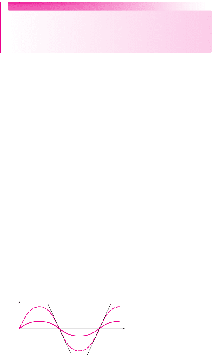
. Figure 14.13 shows two sinusoidal
waveforms of the same frequency but different peak amplitudes. The maximum rate of
v
O
(t)
Time
Slope = –SR Slope = +SR
a
b
Figure 14.13 Two sinusoidal waveforms of the same frequency with different peak voltages,
showing different maximum slopes
nea80644_ch14_1009-1060.qxd 07/12/2009 3:45 Page 1028 pinnacle MHDQ-New:MHDQ134:MHDQ134-14:

change, or slope, occurs as the curves cross the zero axis. The waveform with the larger
peak value has a larger maximum slope. Curve
a
in Figure 14.13 has a maximum slope
corresponding to the slew rate; curve
b
, with a smaller peak value, has a maximum
slope less than the slew rate. If the maximum slope,
ωV
po
, is greater than the slew rate
SR, then the op-amp is slew-rate-limited and the output signal is distorted.
Thus, the maximum frequency at which the op-amp can operate without being
slew-rate-limited is a function of both the frequency and peak amplitude of the signal.
We have that
ω
max
V
po
= 2π f
max
V
po
= SR
(14.54(a))
or
f
max
=
SR
2π V
po
(14.54(b))
As the output voltage peak amplitude increases, the maximum frequency at which
slew-rate-limiting occurs decreases. The full-power bandwidth (FPBW) is the fre-
quency at which the op-amp output becomes slew-rate-limited. The FPBW is the
f
max
frequency from Equation (l4.54(b)), or
FPBW =
SR
2π V
po
(14.55)
The full-power bandwidth can be considerably less than the small-signal bandwidth.
EXAMPLE 14.7
Objective: Determine the small-signal bandwidth of an amplifier and the full-power
bandwidth that will produce an undistorted output voltage.
Consider an amplifier with a unity-gain bandwidth of
f
T
= 1
MHz and a low-
frequency closed-loop gain of
A
CLO
= 10
. Assume the op-amp slew rate is
SR = 1V/μs
and the desired peak output voltage is
V
po
= 10
V.
Solution: The small-signal closed-loop bandwidth is, from Equation (14.44),
f
3-dB
=
f
T
A
CLO
=
10
6
10
⇒ 100 kHz
The full-power bandwidth, based on slew-rate limitation, from Equations (14.54(b))
and (14.55), is
f
max
= FPBW =
SR
2π V
po
=
(1V/μs)(10
6
μs/s)
2π(10)
⇒ 15.9 kHz
Comment: The full-power bandwidth, or the actual maximum frequency at which
the system can be operated and still produce a large, undistorted output signal, is
considerably smaller than the bandwidth under small-signal nonslew-rate-limiting
conditions.
EXERCISE PROBLEM
Ex 14.7: The slew rate of the 741 op-amp is 0.63 V/
μ
s. Determine the full-power
bandwidth for a peak undistorted output voltage of (a) 0.25 V, (b) 2 V, and (c) 8 V.
(Ans. (a) 401 kHz, (b) 50.1 kHz, (c) 12.5 kHz)
Chapter 14 Nonideal Effects in Operational Amplifier Circuits 1029
nea80644_ch14_1009-1060.qxd 07/12/2009 3:45 Page 1029 pinnacle MHDQ-New:MHDQ134:MHDQ134-14:
Test Your Understanding
TYU 14.8 (a) An op-amp is connected in an inverting configuration. The para-
meters of the op-amp are
A
OL
= 5 ×10
4
,
f
PD
= 15
Hz, and
SR = 0.8
V/
μ
s. The
low-frequency closed-loop gain is
|
A
CLO
|
= 25
. (i) What is
f
3-dB
of the closed-loop
system? (ii) If
f
max
= f
3-dB
, determine the maximum undistorted output voltage am-
plitude. (b) Repeat part (a) if the op-amp parameters are
A
OL
= 5 ×10
5
,
f
PD
= 10
Hz, and
SR = 0.8
V/
μ
s. (Ans. (a) (i)
f
3-dB
= 30
kHz, (ii)
V
po
= 4.24
V;
(b) (i)
f
3-dB
= 200
kHz, (ii)
V
po
= 0.637
V)
14.4 OFFSET VOLTAGE
Objective: • Define and analyze sources and effects of offset voltage.
In Chapter 11, we analyzed the basic difference amplifier, which is the input stage of the
op-amp. In that analysis, we assumed the input differential-pair transistors to be identi-
cal, or matched. If the two input devices are mismatched, the currents in the two branches
of the diff-amp are unequal and this affects the diff-amp dc output voltage. In fact, the
internal circuitry of the entire op-amp usually contains imbalances and asymmetries, all
of which can cause a nonzero output voltage for a zero input differential voltage.
The output dc offset voltage is the measured open-loop output voltage when
the input voltage is zero. This configuration is shown in Figure 14.14. The input dc
offset voltage is defined as the input differential voltage that must be applied to the
open-loop op-amp to produce a zero output voltage. This configuration is shown in
Figure 14.15. The input offset voltage is the parameter most often specified and is
usually referred to simply as the offset voltage.
Offset voltage values have a statistical distribution among op-amps of the same
type, and the offset voltage polarity may vary from one op-amp to another. The offset
voltage specification for an op-amp is the magnitude of the maximum offset voltage
for a particular type of op-amp. The offset voltage is a dc value, generally in the range
of 1 to 2 mV for bipolar op-amps, although some op-amps may have offset voltages
in the range of 5 to 10 mV. Further, the maximum offset voltage specification for a
precision op-amp may be as low as 10
μ
V.
In this section we will analyze offset voltage effects in the input diff-amp stage
and will then consider various techniques used to compensate for offset voltage.
Input Stage Offset Voltage Effects
Several possible mismatches in the input diff-amp stage can produce offset voltages.
We will analyze offset voltage effects in two bipolar input stages and in a MOSFET
input diff-amp circuit.
Basic Bipolar Diff-Amp Stage
A basic bipolar diff-amp is shown in Figure 14.16. The differential pair is biased with
a constant-current source. If
Q
1
and
Q
2
are matched, then for
v
1
= v
2
= 0, I
Q
splits
evenly between the two transistors and
i
C1
= i
C2
. If a two-sided output is defined as
14.4.1
1030 Part 2 Analog Electronics
V
OS
+
–
v
O
= 0
+
–
–
+
Figure 14.15 Circuit for
measuring input offset
voltage
+
–
v
O
–
+
Figure 14.14 Circuit for
measuring output offset
voltage
nea80644_ch14_1009-1060.qxd 07/12/2009 3:45 Page 1030 pinnacle MHDQ-New:MHDQ134:MHDQ134-14:
the difference in voltage between the two collector terminals, then
v
O
= 0
when the
transistors are matched and the collector resistors are matched, which means that
the offset voltage is zero.
The collector currents can be written as
i
C1
= I
S1
e
v
BE1
/V
T
(14.56(a))
and
i
C2
= I
S2
e
v
BE2
/V
T
(14.56(b))
where
I
S1
and
I
S2
are related to the reverse-saturation currents in the B–E junctions
and are functions of the electrical and geometric transistor properties. If the two tran-
sistors are exactly matched, then
I
S1
= I
S2
; if there is any mismatch in the electrical
or geometric parameters, then
I
S1
= I
S2
.
The input offset voltage is defined as the input differential voltage required to
produce a zero output voltage, or in this case to produce
i
C1
= i
C2
. Figure 14.17
shows the
i
C
versus
v
BE
characteristics of two unmatched transistors. Slightly dif-
ferent B–E voltages must be applied to produce equal collector currents that will
result in a zero output voltage in the diff-amp.
For
i
C1
= i
C2
, we have
I
S1
e
v
BE1
/V
T
= I
S2
e
v
BE2
/V
T
(14.57)
or
e
(v
BE1
−v
BE2
)/V
T
=
I
S2
I
S1
(14.58)
We define the offset voltage as
v
BE1
−v
BE2
≡ V
OS
Since
v
1
−v
2
= v
BE1
−v
BE2
, then the offset voltage
V
OS
is the differential
input voltage that must be applied to produce
i
C1
= i
C2
.
Equation (14.58) can then be written as
e
V
OS
/V
T
=
I
S2
I
S1
(14.59(a))
Chapter 14 Nonideal Effects in Operational Amplifier Circuits 1031
V
+
V
–
I
Q
R
C
R
C
Q
1
Q
2
v
1
v
2
+
+
–
+
–
–
v
O
v
BE1
v
BE2
i
C1
i
C2
Figure 14.16 Basic bipolar
difference amplifier
i
C
v
BE
V
OS
Figure 14.17 The
i
C
versus
v
BE
characteristics for two unmatched
bipolar transistors
nea80644_ch14_1009-1060.qxd 07/12/2009 3:45 Page 1031 pinnacle MHDQ-New:MHDQ134:MHDQ134-14:

or
V
OS
= V
T
ln
I
S2
I
S1
(14.59(b))
EXAMPLE 14.8
Objective: Calculate the offset voltage in a bipolar diff-amp for a given mismatch
between the input transistors.
Consider the diff-amp in Figure 14.16 with transistor parameters
I
S1
=10
−14
A
and
I
S2
=1.05 ×10
−14
A
.
Solution: From Equation (14.59(b)), the offset voltage is
V
OS
= V
T
ln
I
S2
I
S1
= (0.026) ln
1.05 × 10
−14
1 × 10
−14
= 0.00127 V ⇒ 1.27 mV
Comment: A 5 percent difference in
I
S
for
Q
1
and for
Q
2
produces an offset volt-
age of 1.27 mV. Since the offset voltage is defined as a positive quantity, if in the pre-
vious example
I
S1
were 5 percent larger than
I
S2
, the offset voltage would also be
1.27 mV.
EXERCISE PROBLEM
Ex 14.8: Consider the bipolar diff-amp in Figure 14.16. For
Q
1
, assume
I
S1
= 2 ×10
−15
A. If the offset voltage is
V
OS
= 2
mV, what is the percent dif-
ference in the value of
I
S2
compared to
I
S1
? (Ans. 8 percent)
It should be cautioned that the offset voltage in this example is one component
of the offset voltage for the entire op-amp. For example, if the two collector resistors
are not equal, then the two-sided output voltage
v
O
will not be zero even if the two
transistors are identical. Nevertheless, the calculation provides information on one
source of offset voltage, as well as the resulting magnitude of
V
OS
.
Bipolar Active Load Diff-Amp Stage
Figure 14.18 shows a bipolar diff-amp with a simple two-transistor active load. As
before, this input stage is biased with a constant-current source. If
Q
1
and
Q
2
are
matched and if
Q
3
and
Q
4
are matched, then
I
Q
splits evenly between
Q
1
and
Q
2
for
v
1
= v
2
, and the E–C voltages of
Q
3
and
Q
4
are equal. The one-sided dc output volt-
age
v
O
will therefore be one E–B voltage below
V
+
.
If, however,
Q
3
and
Q
4
are not exactly matched, then
i
C1
and
i
C2
may not be
equal since the active load influences the split in the bias current, even if
Q
1
and
Q
2
are matched. This effect is caused by a finite Early voltage. Taking the Early
voltages into account, but neglecting base currents, we can write the collector
currents as
i
C1
= i
C3
= I
S1
(e
v
BE1
/V
T
)
1 +
v
CE1
V
A1
= I
S3
(e
v
EB3
/V
T
)
1 +
v
EC3
V
A3
(14.60(a))
1032 Part 2 Analog Electronics
nea80644_ch14_1009-1060.qxd 07/12/2009 3:45 Page 1032 pinnacle MHDQ-New:MHDQ134:MHDQ134-14:
and
i
C2
= i
C4
= I
S2
(e
v
BE2
/V
T
)
1 +
v
CE2
V
A2
= I
S4
(e
v
EB4
/V
T
)
1 +
v
EC4
V
A4
(14.60(b))
If we assume that
Q
1
and
Q
2
are matched, then
I
S1
= I
S2
≡ I
S
and
V
A1
=
V
A2
≡ V
AN
. Assume that
Q
3
and
Q
4
are slightly mismatched, so that
I
S3
= I
S4
but
still assume that
V
A3
= V
A4
≡ V
AP
. For
v
1
= v
2
, we have
v
BE1
= v
BE2
; also,
v
EB3
= v
EB4
= v
EC3
≡ v
EB
. Taking the ratio of Equations (14.60(a)) and (14.60(b))
produces
i
C1
i
C2
=
1 +
v
CE1
V
AN
1 +
v
CE2
V
AN
=
I
S3
I
S4
1 +
v
EB
V
AP
1 +
v
EC4
V
AP
(14.61)
Equation (14.61) can be rearranged in the form
1 +
v
CE1
V
AN
1 +
v
EB
V
AP
=
I
S3
I
S4
1 +
v
CE2
V
AN
1 +
v
EC4
V
AP
(14.62)
Since
Q
3
is connected as a diode,
v
CE1
is a constant for a given bias current and
supply voltage, which means that the left side of Equation (14.62) is a constant. If
I
S3
= I
S4
, then
v
CE2
= v
CE1
and
v
EC4
= v
EB
= v
EC3
.However,if
I
S3
= I
S4
, then the
collector–emitter voltages on
Q
2
and
Q
4
must change. If, for example,
I
S3
> I
S4
, then
v
EC4
must increase and
v
CE2
must decrease in order to keep Equation (14.62) balanced.
If, on the other hand,
I
S4
> I
S3
, then
v
CE2
must increase and
v
EC4
must decrease. A
decrease in
v
EC4
means that
Q
4
may be driven into saturation by the mismatch.
Chapter 14 Nonideal Effects in Operational Amplifier Circuits 1033
i
C4
i
C3
v
O
V
+
V
–
I
Q
Q
1
v
1
v
2
Q
2
i
C2
i
C1
Q
4
Q
3
Figure 14.18 Basic bipolar diff-amp with active load
nea80644_ch14_1009-1060.qxd 07/12/2009 3:45 Page 1033 pinnacle MHDQ-New:MHDQ134:MHDQ134-14:

EXAMPLE 14.9
Objective: Calculate the change in output voltage for a given mismatch in the active
load transistors.
Consider the diff-amp in Figure 14.18 with
V
+
= 10
V. Assume that
Q
1
and
Q
2
are matched with
v
BE1
= v
BE2
= 0.6
V, and assume that
v
EB3
= v
EB4
= v
EC3
=
0.6 V. Let
I
S3
= 1.05I
S4
. Also assume that
V
AN
= V
AP
= 50
V.
Solution: Since
v
EB3
= 0.6V= v
BE1
, then for
v
1
= v
2
= 0
,
v
CE1
= V
+
= 10 V
The left side of Equation (14.62) is therefore
1 +
v
CE1
V
AN
1 +
v
EB
V
AP
=
1 +
10
50
1 +
0.6
50
= 1.186
We have that
v
EC4
+v
CE2
= V
+
+v
BE2
= 10.6V
or
v
CE2
= 10.6 −v
EC4
Equation (14.62) then becomes
1.186 = 1.05
1 +
10.6 − v
EC4
50
1 +
v
EC4
50
which yields
v
EC4
= 1.94 V
Comment: A 5 percent difference between the properties of
Q
3
and
Q
4
produces a
change from 0.6 to 1.94 V in the E–C voltage of
Q
4
.
Computer Simulation Verification: A PSpice analysis of the offset voltage effects in
the active load diff-amp was performed. The two input terminals are at ground
potential.
Using
I
S
= 5 ×10
−15
A
for all transistors, the PSpice analysis shows that
v
EB3
= 0.654
V rather than the assumed value of 0.6 V. Also,
v
EC4
is 1.19 V rather
than equal to
v
EB3
. This occurs because the circuit is slightly unbalanced; that is,
i
C1
includes the base currents of
Q
3
and
Q
4
, and
i
C4
does not. When
Q
3
and
Q
4
are not
matched and
I
S3
= 1.05I
S4
= 5.25 ×10
−15
A
, then
v
EC4
increases to 2.51 V, com-
pared to 1.94 V from the hand analysis. If, however,
I
S3
= 0.95I
S4
= 4.75 ×10
−15
A
,
then
Q
4
goes into saturation.
EXERCISE PROBLEM
*Ex 14.9: Consider the active load bipolar diff-amp stage in Figure 14.18. Assume
the circuit and transistor parameters are as given in Example 14.9. Using Equa-
tions (14.60(a)) and (14.60(b)), determine the offset voltage
V
OS
=|v
BE2
−v
BE1
|
such that
v
EC3
= v
EC4
and
v
CE1
= v
CE2
. (Ans. 1.27 mV)
1034 Part 2 Analog Electronics
nea80644_ch14_1009-1060.qxd 07/12/2009 3:45 Page 1034 pinnacle MHDQ-New:MHDQ134:MHDQ134-14:
An offset voltage that will slightly change
i
C1
and
i
C2
will allow the E–C volt-
age of
Q
4
to be adjusted back to its original value.
As shown in actual op-amp circuits, resistors are usually included in the emitters
of the active load transistors. By producing a slight imbalance in the two resistor val-
ues, we can change the ratio of
i
C1
to
i
C2
, causing a change in the output voltage. This
is discussed in the next section when offset voltage null adjustment is discussed.
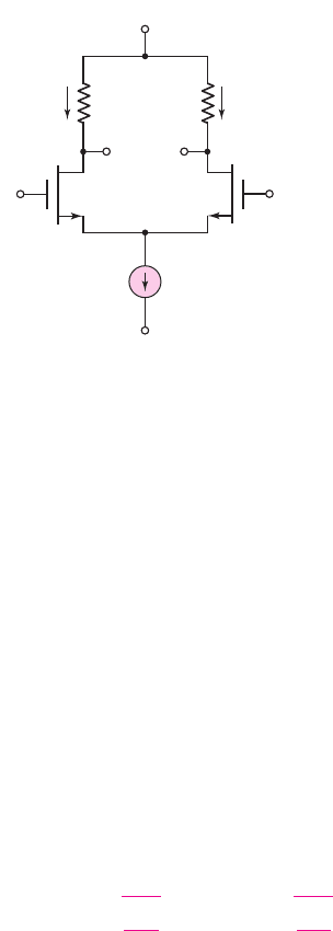
MOSFET Diff-Amp Stage
Figure 14.19 shows a basic MOSFET diff-amp in which the differential pair is biased
with a constant-current source. If
M
1
and
M
2
are matched, then for
v
1
= v
2
= 0, I
Q
splits evenly between the two transistors and
i
D1
= i
D2
. Since a two-sided output is
the voltage difference between the two drain terminals, then for this symmetrical
situation,
v
O
= 0
and the offset voltage is zero.
Chapter 14 Nonideal Effects in Operational Amplifier Circuits 1035
V
+
V
–
I
Q
R
D
R
D
v
2
v
1
+
++
–
––
v
O
v
GS1
v
GS2
i
D1
i
D2
M
1
M
2
Figure 14.19 Basic MOSFET diff-amp
The drain currents can be written as
i
D1
= K
n1
(v
GS1
− V
TN1
)
2
(14.63(a))
and
i
D2
= K
n2
(v
GS2
− V
TN2
)
2
(14.63(b))
As previously stated, the conduction parameters
K
n1
and
K
n2
are functions of
the electrical and geometric properties of the two transistors, and the threshold volt-
ages
V
TN1
and
V
TN2
are also functions of the transistor electrical properties. If there
is a mismatch in electrical or geometric parameters, then we may have
K
n1
= K
n2
and
V
TN1
= V
TN2
.
As with the bipolar diff-amp, the input offset voltage is defined as the input dif-
ferential voltage that must be applied to produce a zero output voltage, or
V
OS
= v
GS1
−v
GS2
(14.64)
When the offset voltage is applied,
i
D1
= i
D2
= I
Q
/2
; when the two drain resistors
are equal, then
v
O
= 0
. Solving Equations (14.63(a)) and (14.63(b)) for
v
GS1
and
v
GS2
and substituting the results into Equation (14.64), we find
V
OS
=
i
D1
K
n1
+ V
TN1
−
i
D2
K
n2
+ V
TN2
(14.65)
nea80644_ch14_1009-1060.qxd 07/12/2009 3:45 Page 1035 pinnacle MHDQ-New:MHDQ134:MHDQ134-14:

The various difference and average quantities are defined as follows:
K
n
= K
n1
− K
n2
(14.66(a))
K
n
=
K
n1
+ K
n2
2
(14.66(b))
V
TN
= V
TN1
− V
TN2
(14.67(a))
and
V
TN
=
V
TN1
+ V
TN2
2
(14.67(b))
Combining Equations (14.66(a)) and (14.66(b)), we have
K
n1
= K
n
+
K
n
2
(14.68(a))
and
K
n2
= K
n
−
K
n
2
(14.68(b))
Similarly,
V
TN1
= V
TN
+
V
TN
2
(14.69(a))
and
V
TN2
= V
TN
−
V
TN
2
(14.69(b))
Noting that
i
D1
= i
D2
= I
Q
/2
and substituting Equations (14.68(a)) through
(14.69(b)) into Equation (14.65), we obtain
V
OS
=
I
Q
2
1
√
K
n
+(K
n
/2)
−
1
√
K
n
−(K
n
/2)
+V
TN
(14.70)
If we assume that
K
n
K
n
then Equation (14.70) reduces to
V
OS
=−
1
2
I
Q
2K
n
·
K
n
K
n
+V
TN
(14.71)
Equation (14.71) is the offset voltage in a MOSFET diff-amp as a function of the
differences in conduction parameters and threshold voltages.
EXAMPLE 14.10
Objective: Calculate the offset voltage in a MOSFET diff-amp stage for a given
mismatch between input transistors.
Consider the diff-amp in Figure 14.19 with transistor parameters
K
n1
=
105 μA/V
2
,
K
n2
= 100 μA/V
2
, and
V
TN1
= V
TN2
. Assume
I
Q
= 200 μ
A.
Solution: From Equation (14.66(a)), the difference in conduction parameters is
K
n
= K
n1
− K
n2
= 105 −100 = 5 μA/V
2
1036 Part 2 Analog Electronics
nea80644_ch14_1009-1060.qxd 07/12/2009 3:45 Page 1036 pinnacle MHDQ-New:MHDQ134:MHDQ134-14:

From Equation (14.66(b)), the average of the conduction parameters is
K
n
=
K
n1
+ K
n2
2
=
105 + 100
2
= 102.5 μA/V
2
The magnitude of the offset voltage is, from Equation (14.71),
|V
OS
|=
1
2
I
Q
2K
n
·
K
n
K
n
=
1
2
200
2(102.5)
5
102.5
= 0.0241 V ⇒ 24.1mV
Comment: A 5 percent difference in conduction parameter values between the input
MOS transistors produces an offset voltage of 24.1 mV.
EXERCISE PROBLEM
Ex 14.10: Assume the MOSFET diff-amp shown in Figure 14.19 is biased with a
current
I
Q
= 150 μA
. Let
V
TN1
= V
TN2
. Assume the nominal conduction para-
meter value is
K
n
= 50 μA/V
2
. Determine the maximum variation
K
n
such that
the offset voltage is limited to
V
OS
= 20
mV. (Ans.
K
n
= 1.63 μA/V
2
)
Comparing the results of Examples 14.8 and 14.10 shows that typically the
offset voltage for a MOSFET diff-amp is substantially larger than that of a bipolar
diff-amp. The difference can be explained by comparing Equation (14.71) for the
MOSFET diff-amp and Equation (14.59(b)) for the bipolar diff-amp. The offset volt-
age for the MOSFET diff-amp is directly proportional to the percent change in
conduction parameter values, whereas the offset voltage for the bipolar diff-amp is
proportional to the logarithm of the percent change in the
I
S
current parameters. In
addition, the offset voltage for the MOSFET pair is proportional to
I
Q
/K
n
= V
GS
− V
TN
which is typically in the range of 0.3–2 V. In contrast, the offset voltage for the bipo-
lar pair is proportional to
V
T
∼
=
26 mV
which is substantially smaller than
(V
GS
− V
TN
)
. Thus, a MOSFET diff-amp inher-
ently displays a higher input offset voltage than a bipolar pair for the same level of
mismatch.
Partial data sheets showing some of the nonideal characteristics for the op-amps
considered in the last chapter are in Table 14.1. The 741 op-amp, an all-bipolar
circuit, has a maximum input offset voltage of 3 mV. The CA3140, which has a
MOSFET input differential pair, has a maximum input offset voltage of 15 mV;
and the LH0042C, which has a JFET input differential pair, has a maximum input
offset voltage of 20 mV. This supports our conclusion that op-amps with FET input
transistors have substantially larger input offset voltages than the all-bipolar cir-
cuit discussed.
Offset Voltage Compensation
In many applications, especially those for which the input signal is large compared to
the offset voltage V
OS
, the effect of the offset voltage is negligible. However, there are
14.4.2
Chapter 14 Nonideal Effects in Operational Amplifier Circuits 1037
nea80644_ch14_1009-1060.qxd 07/12/2009 3:45 Page 1037 pinnacle MHDQ-New:MHDQ134:MHDQ134-14: