Neamen D. Microelectronics: Circuit Analysis and Design
Подождите немного. Документ загружается.

situations in which it is necessary to compensate for, or “null out,” the offset voltage.
Two such methods are: (a) an externally connected offset compensation network,
and (2) an operational amplifier with offset-null terminals.
External Offset Compensation Network
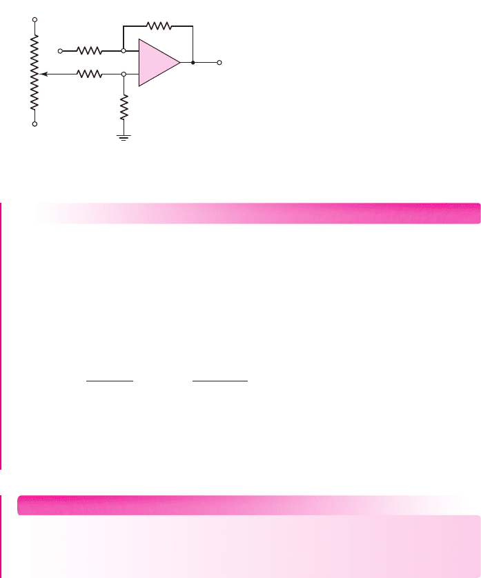
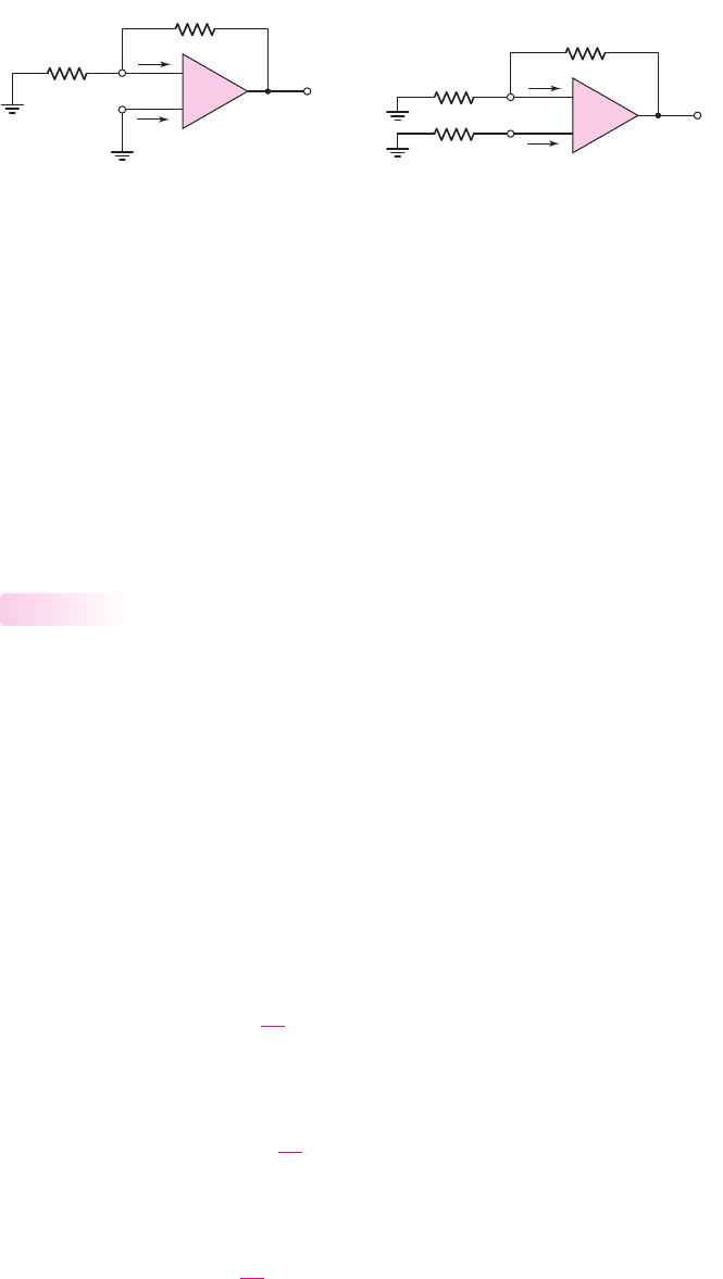
Figure 14.20 shows a simple network for offset voltage compensation in an inverting
amplifier. The resistive voltage divider of
R
4
and
R
5
, in conjunction with poten-
tiometer
R
3
, is used to make voltage adjustments of either polarity at the noninvert-
ing terminal to cancel the effects of
V
OS
. If
R
5
R
4
, then the compensating voltage
applied to the noninverting terminal can be in the millivolt range, which is typical of
offset voltage values.
1038 Part 2 Analog Electronics
R
1
R
2
R
3
V
X
V
Y
v
O
v
I
R
4
–
+
R
5
V
–
V
+
Figure 14.20 Offset voltage compensation circuit for inverting amplifier
EXAMPLE 14.11
Objective: Determine the range of voltage produced by an offset voltage compensa-
tion network.
Consider the compensation network in Figure 14.20 with
R
5
= 100
,
R
4
=
100 k
, and a 100 k
potentiometer
R
3
. Let
V
+
= 15
V and
V
−
=−15 V
. Deter-
mine the voltage range at
V
Y
.
Solution: Assume the potentiometer wiper arm is connected to the
V
+
supply volt-
age. The voltage
V
Y
is then
V
Y
=
R
5
R
5
+ R
4
V
+
=
0.1
0.1 + 100
(15) ⇒ 15 mV
Comment: For this particular circuit, the compensation voltage range is
−15 mV
to
+15
mV. A larger resistance
R
5
will increase the offset voltage compensation
range, and a smaller resistance
R
5
will increase the sensitivity of offset voltage
compensation.
EXERCISE PROBLEM
Ex 14.11: Consider the compensation network in Figure 14.20. Assume
V
+
=
10 V,
V
−
=−10 V
,
R
3
= 100 k
, and
R
4
= 100 k
. Design
R
5
such that the circuit
can compensate for an offset voltage of
V
OS
= 5
mV. (Ans. 50
)
Figure 14.21 shows a compensation network that can be used with a noninverting
op-amp circuit. The same
R
4
–
R
5
voltage divider is used with the potentiometer
R
3
.
Typically,
R
5
is on the order of
100
and
R
4
on the order of
100 k
. If
V
+
= 15
V
nea80644_ch14_1009-1060.qxd 07/12/2009 3:45 Page 1038 pinnacle MHDQ-New:MHDQ134:MHDQ134-14:
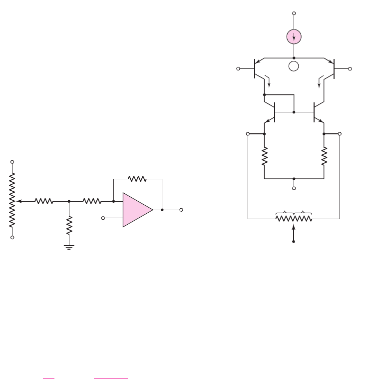
and
V
−
=−15 V
, then the compensation voltage is again in the range of
−15 mV
to
+15
mV.
The voltage gain of the noninverting amplifier becomes a function of the com-
pensation network. Since
R
5
R
4
, then the gain of the amplifier, to a good approx-
imation, is
A
v
=
v
O
v
I
=
1 +
R
2
R
1
+ R
5
(14.72)
Since
R
5
is small, Equation (14.72) shows that the gain is not a strong function of the
compensation network; however, it may still need to be taken into account.
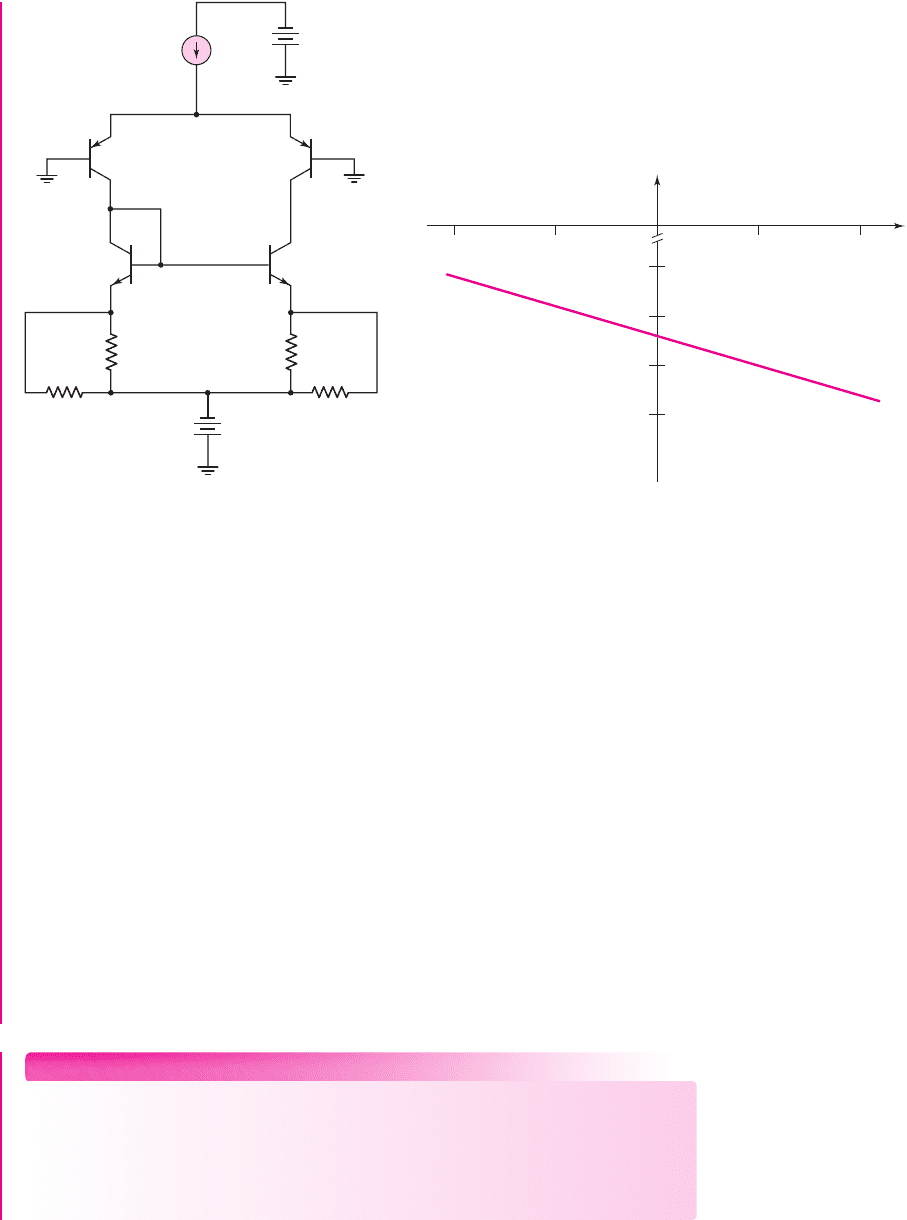
Offset-Null Terminals
Many op-amps, including the 741 bipolar and the CA3140 BiCMOS circuits studied
in Chapter 13, include a pair of external offset-null terminals, which are used to com-
pensate for the offset voltage. Figure 14.22 shows a basic bipolar input diff-amp stage,
including a pair of offset-null terminals. An external potentiometer
R
x
is connected
between these terminals, and the wiper arm is connected to supply voltage
V
−
.
If the wiper arm of
R
x
is centered, then
R
1
and
R
2
will each have a resistance
R
x
/2
connected in parallel. When the wiper arm is moved off center, then
R
1
and
R
2
will each have a different resistance connected in parallel, and an asymmetry will be
introduced into the circuit. This asymmetry in turn introduces an offset voltage,
which cancels the input offset voltage effects. In practice, to adjust for offset voltage
effects, the op-amp is connected in a feedback configuration with the input differen-
tial voltage set equal to zero. The wiper arm of potentiometer
R
x
is then adjusted
until the output voltage becomes zero.
Chapter 14 Nonideal Effects in Operational Amplifier Circuits 1039
R
2
v
O
v
I
R
4
= 100 kΩ
R
5
= 100 Ω
R
1
R
3
V
–
V
+
–
+
Figure 14.21 Offset voltage compensation circuit
for noninverting amplifier
V
+
V
–
V
–
I
Q
R
x
x
1 – x
Q
3
R
1
R
2
Q
4
i
C1
i
C2
v
2
v
1
3
Q
2
Q
1
++
––
v
BE3
v
BE4
Offset-
null
terminal
Offset-
null
terminal
Figure 14.22 Basic bipolar input diff-amp stage, including
a pair of offset-null terminals connected to a potentiometer
nea80644_ch14_1009-1060.qxd 07/12/2009 3:45 Page 1039 pinnacle MHDQ-New:MHDQ134:MHDQ134-14:

To demonstrate the offset-null technique, we first write a KVL equation between
the base terminals of
Q
3
and
Q
4
and voltage
V
−
in Figure 14.22, as follows:
v
BE3
+i
C1
R
1
= v
BE4
+i
C2
R
2
(14.73)
where
R
1
and
R
2
are the effective resistances in the emitters of
Q
3
and
Q
4
, including
the parallel effects of potentiometer
R
x
. We have that
R
1
= R
1
xR
x
and R
2
= R
2
(1 − x)R
x
The base–emitter voltages are
v
BE3
= V
T
ln
i
C1
I
S3
(14.74(a))
and
v
BE4
= V
T
ln
i
C2
I
S4
(14.74(b))
Substituting Equations (14.74(a)) and (14.74(b)) into Equation (14.73) yields
V
T
ln
i
C1
I
S3
+i
C1
R
1
= V
T
ln
i
C2
I
S4
+i
C2
R
2
(14.75)
If a mismatch occurs between
Q
3
and
Q
4
, meaning
I
S3
= I
S4
, then a deliberate
mismatch between
R
1
and
R
2
can be introduced to compensate for the transistor
mismatch and the adjustment can make
i
C1
= i
C2
. Similarly, a deliberate mismatch
between
R
1
and
R
2
can be used to compensate for a mismatch between
Q
1
and
Q
2
.
EXAMPLE 14.12
Objective: Determine the required difference between
R
1
and
R
2
, and the value of
x
in the potentiometer to compensate for a mismatch between active load transistors
Q
3
and
Q
4
in the diff-amp in Figure 14.22.
Assume that
I
Q
= 200 μA
, which means that we want
i
C1
= i
C2
= 100 μA
. Let
I
S3
= 10
−14
A
and
I
S4
= 1.05 ×10
−14
A
. Also assume
R
1
= R
2
= 1k
and
R
x
= 100 k
.
Solution: The difference between
R
2
and
R
1
is determined from Equation (14.75),
as follows:
V
T
ln
i
C1
I
S3
+i
C1
R
1
= V
T
ln
i
C2
I
S4
+i
C2
R
2
or
(0.026) ln
100 × 10
−6
10
−14
+(0.10)R
1
= (0.026) ln
100 × 10
−6
1.05 × 10
−14
+(0.10)R
2
which yields
R
2
− R
1
= 0.0127 k ⇒ 12.7
We can also write the difference between
R
2
and
R
1
as
R
2
(1 − x)R
x
R
2
+(1 − x)R
x
−
R
1
xR
x
R
1
+ xR
x
= 0.0127 k
1040 Part 2 Analog Electronics
nea80644_ch14_1009-1060.qxd 07/12/2009 3:45 Page 1040 pinnacle MHDQ-New:MHDQ134:MHDQ134-14:
Substituting the values for
R
1
, R
2
, and
R
x
, we find that
x = 0.349
Comment: On the basis of this analysis, the value of
R
1
is
134.9 = 0.9721 k
, and
the value of
R
2
is
1(100 − 34.9) = 0.9849 k
.
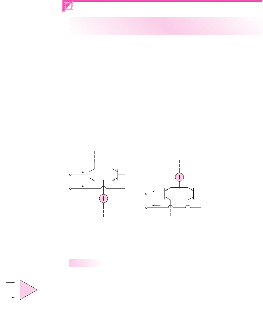
Computer Simulation Verification: Figure 14.23 is the circuit used in PSpice simu-
lation. The values of
R
X
and
R
Y
were varied to simulate a change in the variable x in
the potentiometer in the circuit in Figure 14.22. The output voltage
v
O
is taken off the
common collectors of
Q
1
and
Q
3
. This voltage would correspond to the input volt-
age of a second stage.
A change in the values of
R
X
and
R
Y
causes a slight change in the currents in the
two sides of the circuit. A change in current causes a change in the collector–emitter
voltages of
Q
1
and
Q
3
, or a change in the output voltage. Figure 14.24 shows the out-
put voltage as a function of
x
, or as a function of the position of the potentiometer.
The results show that a change of approximately 0.7 V is possible for this range in
potentiometer setting. This change in voltage would represent a large change in input
voltage for the second stage, which in turn would cause a large change in the dc value
of the output voltage. The dc output voltage could therefore be set to zero by adjust-
ing the potentiometer setting.
Chapter 14 Nonideal Effects in Operational Amplifier Circuits 1041
Q
2
2N3906
Q
1
2N3906
Q
3
2N3904
Q
4
2N3904
200 mA
5 V
0
00
+
–
I
1
V
1
5 V
0
–
+
V
6
R
2
1 kΩ
R
Y
50 kΩ
R
X
50 kΩ
R
1
1 kΩ
I
DC
Figure 14.23 Circuit used in the computer
simulation analysis for Example 14.12
v
o
(V)
0.3 0.4 0.6
–3.5
–3.75
– 4.0
– 4.25
0.5 0.7
x
Figure 14.24 Output voltage versus potentiometer setting
EXERCISE PROBLEM
*Ex 14.12: Consider the diff-amp in Figure 14.22 with a pair of offset-null ter-
minals. Let
R
1
= R
2
= 1
k
. Let R
x
be a 100 k
potentiometer. Assume
I
Q
=
100 μA and
I
S3
= 10
−14
A
. If the wiper arm on the potentiometer is adjusted such
that 25 k
is in parallel with R
1
and 75 k
is in parallel with R
2
, determine the
value of I
S4
for
i
C1
= i
C2
. (Ans.
1.05 × 10
−14
A
)
nea80644_ch14_1009-1060.qxd 07/12/2009 3:45 Page 1041 pinnacle MHDQ-New:MHDQ134:MHDQ134-14:
14.5 INPUT BIAS CURRENT
Objective: • Define and analyze effects of input bias currents.
The input currents to an ideal op-amp are zero. In actual operational amplifiers, how-
ever, the input bias currents are not zero. If the input stage consists of a pair of npn
transistors, as shown in Figure 14.25(a), the bias currents enter the input terminals.
However, if the input state consists of a pair of pnp transistors, as shown in Fig-
ure l4.25(b), the bias currents leave the input terminals.
If the input diff-amp consists of a pair of JFETs, the input bias currents are nor-
mally much smaller than those in a bipolar differential pair. A MOSFET input dif-
ferential pair, generally, must include protection devices as discussed in Chapter 13,
so the input bias currents are also not zero even in this case.
For op-amps with a bipolar input stage, the input bias currents may be as high as
10
μ
A and as low as a few nanoamperes. For op-amps with an FET input stage, the
bias currents may be as low as a few picoamperes. Table 14.1 lists the typical input
bias current. For the 741 op-amp it is 30 nA, and for the FET input op-amps it is in
the low picoampere range.
1042 Part 2 Analog Electronics
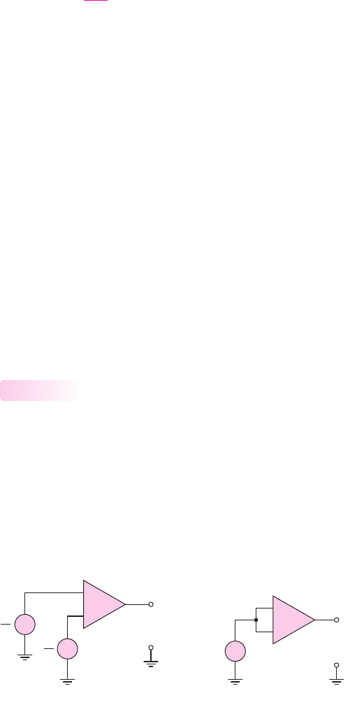
I
B1
I
B2
I
Q
Q
1
Q
2
I
B1
I
B2
I
Q
Q
1
Q
2
(a) (b)
Figure 14.25 (a) Pair of npn transistors, showing input bias currents, and (b) pair of pnp
transistors, showing input bias currents
I
B1
I
B2
–
+
Figure 14.26 Op-amp with
input bias currents
Bias Current Effects
Figure 14.26 schematically shows an op-amp with input bias currents. If the input
stage is symmetrical, with all corresponding elements matched, then
I
B1
= I
B2
.
However, if the input transistors are not exactly identical, then
I
B1
= I
B2
. The input
bias current is then defined as the average of the two input currents, or
I
B
=
I
B1
+ I
B2
2
(14.76)
The difference between the two input currents is called the input offset current
I
OS
and is given by
I
OS
=|I
B1
− I
B2
|
(14.77)
14.5.1
nea80644_ch14_1009-1060.qxd 07/12/2009 3:45 Page 1042 pinnacle MHDQ-New:MHDQ134:MHDQ134-14:
Chapter 14 Nonideal Effects in Operational Amplifier Circuits 1043
R
2
R
1
V
Y
v
O
V
X
I
B1
I
B2
–
+
Figure 14.27 Op-amp with grounded
noninverting terminal
R
2
R
1
V
Y
v
O
V
X
I
B1
I
B2
–
+
R
3
Figure 14.28 Op-amp circuit with resistor connected to
noninverting terminal, for input bias current compensation
The algebraic sign of the offset current is usually not important, just as the offset
voltage polarity is not critical. The typical input offset current is on the order of
10 percent of the input bias current, although data sheets may list larger values. The
typical and maximum input offset currents for the three op-amps analyzed in the last
chapter are given in Table 14.1.
Figure 14.27 shows an op-amp and associated resistors for a zero input voltage.
Even if
I
B2
= 0
, the noninverting terminal is still at zero volts, or
V
Y
= 0
. From the
virtual ground concept, we have
V
X
= 0
, which means that the current in R
1
must be
zero. Bias current I
B1
is therefore supplied by the output of the op-amp and flows
through R
2
, producing an output voltage. If, for example,
I
B1
= 5 μ
A and
R
2
=
100 k
, then
v
O
= 0.5
V, which is unacceptable in most applications. Smaller input
bias currents and a smaller feedback resistor will reduce the bias current effects.
Bias Current Compensation
The effect of bias currents in op-amp circuits can be minimized with a simple com-
pensation technique. Consider the circuit in Figure 14.28. We determine
v
O
as a
function of I
B1
and I
B2
using superposition. For
I
B2
= 0
, then
V
Y
= V
X
= 0
, and the
output voltage due to I
B1
is
v
O
(I
B1
) = I
B1
R
2
(14.78(a))
For
I
B1
= 0
, we find
V
Y
=−I
B2
R
3
= V
X
Since
v
O
= (1 + R
2
/R
1
)V
X
the output voltage due to I
B2
is
v
O
(I
B2
) =−I
B2
R
3
1 +
R
2
R
1
(14.78(b))
The net output voltage due to both I
B1
and I
B2
is the sum of Equations (14.78(a))
and (14.78(b)), or
v
O
= I
B1
R
2
− I
B2
R
3
1 +
R
2
R
1
(14.79)
If
I
B1
= I
B2
≡ I
B
and if the combination of the three resistances can be adjusted
to produce
v
O
= 0
, then Equation (14.79) becomes
0 = I
B
R
2
− R
3
1 +
R
2
R
1
(14.80)
14.5.2
nea80644_ch14_1009-1060.qxd 07/12/2009 3:45 Page 1043 pinnacle MHDQ-New:MHDQ134:MHDQ134-14:

which means that
R
2
= R
3
1 +
R
2
R
1
(14.81)
Equation (14.81) can be rearranged as follows:
R
3
=
R
1
R
2
R
1
+ R
2
= R
1
R
2
(14.82)
Equation (14.82) shows that R
3
should be made equal to the parallel combination
of R
1
and R
2
, to eliminate the effect of equal input bias currents.
If
R
3
= R
1
R
2
and if the bias currents are not equal, then from Equation (14.79),
we have
v
O
= R
2
(
I
B1
− I
B2
)
= R
2
I
OS
(14.83)
Since the input offset current is normally a fraction of the input bias current,
Equation (14.83) shows that the bias current effect can be reduced by making
R
3
= R
1
R
2
.
EXAMPLE 14.13
Objective: Determine the bias current effect in an op-amp circuit, with and without
bias current compensation.
Consider the op-amp circuits in Figures 14.27 and 14.28. Let
R
1
= 10
k
and
R
2
= 100
k
. Assume
I
B1
= 1.1 μ
A and
I
B2
= 1.0 μ
A.
Solution: For the op-amp circuit in Figure 14.27, the output voltage due to the bias
currents is
v
O
= I
B1
R
2
= (1.1 ×10
−6
)(100 × 10
3
) = 0.11 V
For the circuit in Figure 14.28, we design R
3
such that
R
3
= R
1
R
2
= 10100 = 9.09 k
Then, from Equation (14.83), we find
v
O
= R
2
(I
B1
− I
B2
) = (100 ×10
3
)(1.1 − 1.0) × 10
−6
= 0.010 V
Comment: Even if the input offset current is not zero, the effect of the input bias
currents can be reduced substantially by incorporating resistor R
3
.
EXERCISE PROBLEM
Ex 14.13: For the op-amp circuit shown in Figure 14.28, the parameters are
R
1
= 20
k
and
R
2
= 120
k
. (a) Let
I
B1
= I
B2
= 0.8 μ
A. (i) Can
R
3
be ad-
justed such that
v
O
= 0
? (ii) If so, what is the value of
R
3
? (b) Repeat part (a) if
I
B1
= 0.75 μ
A and
I
B2
= 0.85 μ
A. (Ans. (a)
R
3
= 17.14
k
,(b)
R
3
= 15.13
k
)
Usually the effect of bias currents in op-amp circuits is significant only for cir-
cuits with large resistor values. For these situations, an op-amp with an FET input
stage may be necessary.
1044 Part 2 Analog Electronics
nea80644_ch14_1009-1060.qxd 07/12/2009 3:45 Page 1044 pinnacle MHDQ-New:MHDQ134:MHDQ134-14:
Test Your Understanding
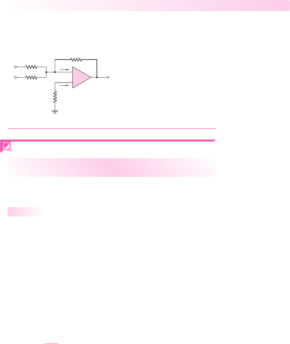
TYU 14.9 Consider the inverting summing amplifier in Figure 14.29. Assume input
bias currents of
I
B1
= I
B2
= 1.1
μA. (a) For
v
i1
= v
i2
= 0
and
R
4
= 0
, determine
v
O
due to the bias currents. (b) Find the value of R
4
that compensates for the effects
of the bias currents. (Ans. (a)
v
O
= 0.22
V (b)
R
4
= 28.6
k
)
Chapter 14 Nonideal Effects in Operational Amplifier Circuits 1045
R
3
= 200 kΩ
R
1
= 100 kΩ
v
O
I
B1
I
B2
–
+
R
2
= 50 kΩ
v
I1
v
I2
R
4
Figure 14.29 Figure for Exercise TYU14.9
14.6 ADDITIONAL NONIDEAL EFFECTS
Objective: • Discuss and analyze additional nonideal effects.
Two additional nonideal effects in op-amps are: temperature effects and common-
mode rejection ratio. We will look at each of these in this section.
Temperature Effects
Individual transistor parameters are functions of temperature. For bipolar transistors,
the collector current is
i
C
= I
S
e
v
BE
/V
T
(14.84)
where both I
S
and V
T
are functions of temperature. We expect the open-loop gain to
vary with temperature, but as we saw in Section 14.2, the fractional change in the
closed-loop gain is orders of magnitude less than the fractional change in the open-
loop gain. This then makes the closed-loop gain very insensitive to temperature
variations.
Offset Voltage Temperature Coefficient
Since the electrical properties of transistors are functions of temperature, the input
offset voltage is also a function of temperature. The rate of change of offset voltage
with temperature is defined as the temperature coefficient of offset voltage, or
input offset voltage drift, and is given by
TCv
OS
=
dV
OS
dT
(14.85)
For a bipolar diff-amp input stage, the offset voltage, from Equation (14.59(b)), is
V
OS
= V
T
ln(I
S2
/I
S1
)
14.6.1
nea80644_ch14_1009-1060.qxd 07/12/2009 3:45 Page 1045 pinnacle MHDQ-New:MHDQ134:MHDQ134-14:
The temperature variations of the I
S
parameters cancel; therefore, the offset voltage
is directly proportional to the thermal voltage V
T
, which in turn is directly propor-
tional to temperature. From Equation (14.59(b)), the temperature coefficient is then
TCv
OS
=
V
OS
T
(14.86)
where T is the absolute temperature. Thus, for
V
OS
= 1
mV, the temperature coeffi-
cient is
TCv
OS
= 1mV/300 K ⇒ 3.3 μV/
◦
C
. A change of
10
◦
C
will therefore
result in an offset voltage change of approximately 33
μ
V. The temperature coeffi-
cients of offset voltage listed in Table 14.1 are in the range of 10 to 15
μ
V/°C.
Consequently, the offset voltage compensation techniques discussed previously
are completely effective at only one temperature. As the device temperature drifts in
either direction from the temperature at which the compensation network was de-
signed, the offset voltage effect is not completely compensated. However, the offset
voltage drift is substantially less than the initial offset voltage, so offset voltage com-
pensation is still desirable.
Input Offset Current Temperature Coefficient
The input bias currents are functions of temperature. For example, the input bias cur-
rent of a bipolar input stage has the same functional dependence as the collector
current, as given by Equation (14.84). If the input devices are not matched, then an
input offset current I
OS
exists, which is also a function of temperature. The input
offset current temperature coefficient is dI
OS
/dT. For the 741 op-amp, the maximum
value given in Table 14.1 is 0.5 nA/°C. If the input offset current becomes a problem
in a particular design, then a JFET of MOSFET input stage op-amp may be required.
Common-Mode Rejection Ratio
We considered the common-mode gain (A
cm
) and common-mode rejection ratio
(CMRR) of the difference amplifier in Chapter 11. Since a diff-amp is the op-amp
input stage, any common-mode signal produced at the input stage will propagate
through the op-amp to the output. Therefore, the CMRR of the op-amp is essentially
the same as the CMRR of the input diff-amp.
Figure 14.30(a) shows the open-loop op-amp with a pure differential-mode input
signal. The differential-mode gain A
d
is the same as the open-loop gain A
OL
. Figure
14.30(b) shows the open-loop op-amp with a pure common-mode input signal.
14.6.2
1046 Part 2 Analog Electronics
(a) (b)
+
–
v
o
= A
cm
v
cm
v
cm
+
–
–
+
+
–
v
o
= A
d
v
d
v
d
2
v
d
2
+
–
–
+
–
+
Figure 14.30 Open-loop op-amp (a) with pure differential-mode input signal and (b) with
pure common-mode input signal
nea80644_ch14_1009-1060.qxd 07/12/2009 3:45 Page 1046 pinnacle MHDQ-New:MHDQ134:MHDQ134-14:
The common-mode rejection ratio, in dB, is
CMRR
dB
= 20 log
10
A
d
A
cm
(14.87)
Typical values of CMRR
dB
range from 80 to 100 dB. Table 14.1 lists typical
CMRR
dB
values for three op-amps.
14.7 DESIGN APPLICATION: AN OFFSET VOLTAGE
COMPENSATION NETWORK
Objective: • Design an offset voltage compensation network for a
CMOS diff amp.
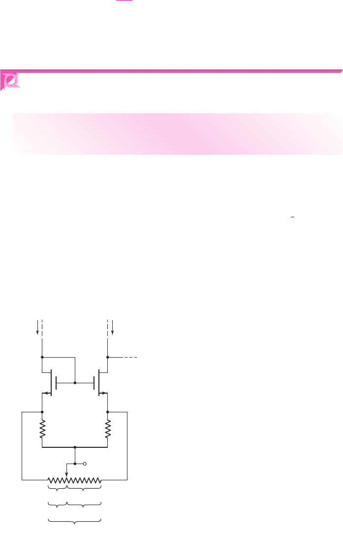
Specifications: An offset voltage compensation network is to be designed at the
active load of a CMOS diff-amp.
Design Approach: An offset voltage compensation network with the configuration
shown in Figure 14.31 is to be designed. Assume both a 5 percent and
2
1
2
percent dif-
ference in conduction parameters between M
1
and M
2
. This mismatch will demon-
strate how the network can compensate for an offset voltage.
Choices: For both M
1
and M
2
, assume parameters
V
TN
= 0.5
V,
W/L = 20
, and
λ
n
= 0.02 V
−1
. For M
1
, assume
k
n1
= 80 μA/V
2
and for M
2
, assume (i)
k
n2
=
76 μA/V
2
and then (ii)
k
n2
= 78 μA/V
2
. A 50 k
center-tapped potentiometer is
available.
Chapter 14 Nonideal Effects in Operational Amplifier Circuits 1047
V
–
= –15 V
R
1
=
1 kΩ
50 kΩ
R
2
=
1 kΩ
+
++
–
–
–
M
1
M
2
V
DS2
V
GS1
R
A
I – x x
R
B
V
GS2
100 mA 100 m
A
Figure 14.31 An offset voltage compensation network for the design application
nea80644_ch14_1009-1060.qxd 07/12/2009 3:45 Page 1047 pinnacle MHDQ-New:MHDQ134:MHDQ134-14: