Neamen D. Microelectronics: Circuit Analysis and Design
Подождите немного. Документ загружается.


1178 Part 3 Digital Electronics
Solution: From Equation (16.52), power dissipation in the CMOS inverter is
P = fC
L
V
2
DD
= (10
5
)(2 × 10
−12
)(5)
2
⇒ 5 μW
Comment: Previously determined values of static power dissipation in NMOS in-
verters were on the order of 500
μ
W; therefore, power dissipation in a CMOS
inverter is substantially smaller. In addition, in most digital systems, only a small
fraction of the logic gates change state during each clock cycle; consequently, the
power dissipation in a CMOS digital system is substantially less than in an NMOS
digital system of similar complexity.
EXERCISE PROBLEM
Ex 16.8: A CMOS inverter is biased at
V
DD
= 3V
. The inverter drives an effec-
tive load capacitance of
C
L
= 0.5pF
. Determine the maximum switching fre-
quency such that the power dissipation is limited to
P = 0.10 μW
. (Ans.
f =
22.2 kHz
)
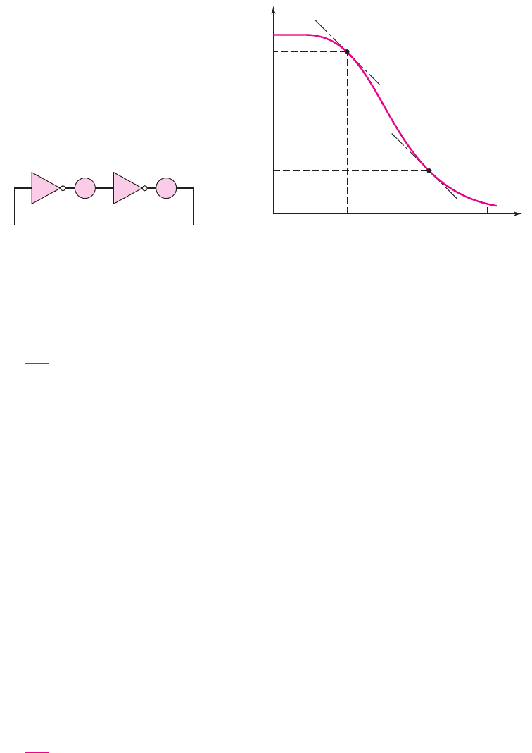
Noise Margin
The word “noise” means transient, unwanted variations in voltages or currents. In dig-
ital circuits, if the magnitude of the noise at a logic node is too large, logic errors can
be introduced into the system. However, if the noise amplitude is less than a specified
value, called the noise margin, the noise signal will be attenuated as it passes through
a logic gate or circuit, while the logic signals will be transmitted without error.
Noise signals are usually generated outside the digital circuit and transferred
to logic nodes or interconnect lines through parasitic capacitances or inductances.
The coupling process is usually time dependent, leading to dynamic conditions in
the circuit. In digital systems, however, the noise margins are usually defined in
terms of static voltages.
Noise Margin Definition
For static noise margins, the type of noise usually considered is called series-voltage
noise. Figure 16.30 shows two inverters in series in which the output of the second is
connected back to the input of the first. Also included are series-voltage noise sources
δV
L
and
δV
H
. This type of noise can be developed by inductive coupling. The input
voltage levels are indicated by H (high) and L (low). The noise amplitudes
δV
L
and
δV
H
can be different, and the polarities may be such as to increase the low output and
reduce the high output. The noise margins are defined as the maximum values of
δV
L
and
δV
H
at which the inverters will remain in the correct state.
The actual definitions of the noise margins
NM
L
and
NM
H
are not unique. In ad-
dition other types of noise, other than series-voltage source noise, may be present in
the system. Dynamic noise sources also complicate the issue. However, in this text,
in order to provide some measure of noise margin in a logic circuit, we will use the
unity-gain approach to determine the logic threshold levels
V
IL
and
V
IH
and the cor-
responding noise margins.
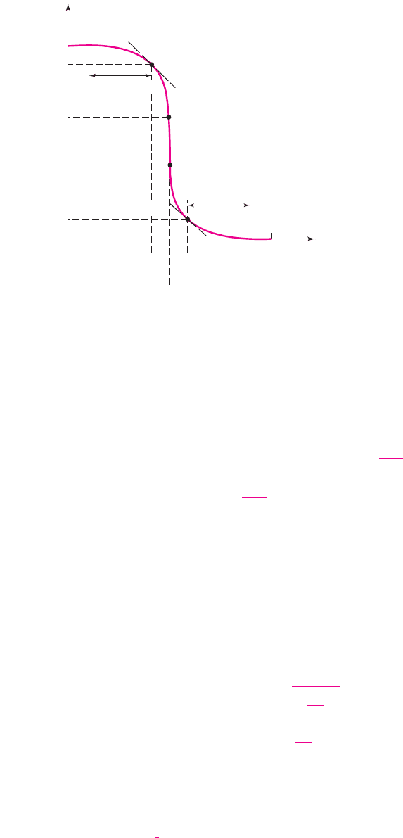
Figure 16.31 shows a general voltage transfer function for an inverter. The ex-
pected logic 1 and logic 0 output voltages of the inverter are
V
OH
and
V
OL
, respec-
16.3.4
nea80644_ch16_1145-1254.qxd 07/12/2009 3:37 Page 1178 pinnacle MHDQ-New:MHDQ134:MHDQ134-16:
Chapter 16 MOSFET Digital Circuits 1179
tively. The parameters
V
IH
and
V
IL
, which determine the noise margins, are defined
as the points at which
dv
O
dv
I
=−1
(16.53)
For
v
I
≤ V
IL
, the inverter gain magnitude is less than unity, and the output
changes slowly with a change in the input voltage. Similarly, for
v
I
≥ V
IH
, the out-
put again changes slowly with input voltage since the gain magnitude is less than
unity. However, when the input voltage is in the range
V
IL
<v
I
< V
IH
, the gain
magnitude is greater than one, and the output signal changes rapidly. This region is
called the undefined range. If the input voltage is inadvertently pushed into this
range by a noise signal, the output may change logic states, and a logic error could be
introduced into the system. The corresponding output voltages at the unity-gain
points are denoted
V
OHU
and
V
OLU
, where the last subscript U signifies the unity-
gain values.
The noise margins are defined as
NM
L
= V
IL
− V
OLU
(16.54(a))
and
NM
H
= V
OHU
− V
IH
(16.54(b))
Figure 16.32 shows the general voltage transfer function of a CMOS inverter.
(The numbers in the figure are from Example 16.9 to be considered later.) The
parameters
V
IH
and
V
IL
determine the noise margins and are defined as the points at
which
dv
O
dv
I
=−1
(16.55)
For
v
I
≤ V
IL
and
v
I
≥ V
IH
, the gain is less than unity and the output changes slowly
with input voltage. However, when the input voltage is in the range
V
IL
<v
I
< V
IH
,
the inverter gain is greater than unity, and the output signal changes rapidly with a
change in the input voltage. This is the undefined range.
LHH
d V
L
d V
H
V
1
V
2
V
1
G
1
G
2
+
–
–
+
Figure 16.30 Two-inverter flip-flop,
including series-voltage noise sources
v
O
v
I
V
IL
V
IH
V
OH
V
OL
V
OLU
V
OHU
V
OH
dv
O
dv
I
= –1
dv
O
dv
I
= –1
Figure 16.31 Generalized inverter voltage curve and
defined voltage limits
V
IL
and
V
IH
nea80644_ch16_1145-1254.qxd 07/12/2009 3:37 Page 1179 pinnacle MHDQ-New:MHDQ134:MHDQ134-16:
1180 Part 3 Digital Electronics
Point
V
IL
occurs when the NMOS is biased in the saturation region and the
PMOS is biased in the nonsaturation region. The relationship between the input and
output voltages is given by Equation (16.35). Taking the derivative with respect to
v
I
yields
2K
n
[v
I
− V
TN
] = K
p
−2(V
DD
−v
O
) − 2(V
DD
−v
I
+ V
TP
)
dv
O
dv
I
−2(V
DD
−v
O
)
−
dv
O
dv
I
(16.56)
Setting the derivative equal
−1
, we have
K
n
[v
I
− V
TN
] =−K
p
[(V
DD
−v
O
) − (V
DD
−v
I
+ V
TP
) + (V
DD
−v
O
)]
(16.57)
Solving for
v
O
produces
v
O
= V
OHU
=
1
2
1 +
K
n
K
p
v
I
+ V
DD
−
K
n
K
p
V
TN
− V
TP
(16.58)
Combining Equations (16.58) and (16.35), we see that voltage
V
IL
is
v
I
= V
IL
= V
TN
+
(V
DD
+ V
TP
− V
TN
)
K
n
K
p
−1
⎡
⎢
⎢
⎢
⎣
2
K
n
K
p
K
n
K
p
+3
−1
⎤
⎥
⎥
⎥
⎦
(16.59)
If
K
n
= K
p
, Equation (16.59) becomes indefinite, since a zero would exist in
both the numerator and the denominator. However, when
K
n
= K
p
, Equation (16.58)
becomes
v
O
= V
OHU(K
n
=K
p
)
=
1
2
{2v
I
+ V
DD
− V
TN
− V
TP
}
(16.60)
V
OLU
= 0.3125
1.25
2.05
V
IH
=
1.9625 V
V
OHU
V
OLU
V
It
= 1.65 V
V
IL
=
1.3375 V
V
OHU
= 2.9875
V
OH
= 3.3
3.3
0
Slope = –1
Slope = –1
NM
H
= 1.025
v
O
(V)
v
I
(V)
NM
L
= 1.025 V
Figure 16.32 CMOS inverter voltage transfer characteristics with defined noise margins
nea80644_ch16_1145-1254.qxd 07/12/2009 3:37 Page 1180 pinnacle MHDQ-New:MHDQ134:MHDQ134-16:

Chapter 16 MOSFET Digital Circuits 1181
Substituting Equation (16.60) into Equation (16.35) yields a voltage
V
IL
of
v
I
= V
IL(K
n
=K
p
)
= V
TN
+
3
8
(V
DD
+ V
TP
− V
TN
)
(16.61)
for
K
n
= K
p
.
Point
V
IH
occurs when the NMOS is biased in the nonsaturation region and the
PMOS is biased in the saturation region. The relationship between the input and
output voltages is given by Equation (16.43). Taking the derivative with respect to
v
I
yields
K
n
2(v
I
− V
TN
)
dv
O
dv
I
+2v
O
−2v
O
dv
O
dv
I
= 2K
p
(V
DD
−v
I
+ V
TP
)(−1)
(16.62)
Setting the derivative equal to
−1
, we find that
K
n
[−(v
I
− V
TN
) + v
O
+v
O
] =−K
p
[V
DD
−v
I
+ V
TP
]
(16.63)
The output voltage
v
O
is then
v
O
= V
OLU
=
v
I
1 +
K
n
K
p
− V
DD
−
K
n
K
p
V
TN
− V
TP
2
K
n
K
p
(16.64)
Combining Equations (16.64) and (16.43), yields voltage
V
IH
as
v
I
= V
IH
= V
TN
+
(V
DD
+ V
TP
− V
TN
)
K
n
K
p
−1
⎡
⎢
⎢
⎢
⎢
⎣
2
K
n
K
p
3
K
n
K
p
+1
−1
⎤
⎥
⎥
⎥
⎥
⎦
(16.65)
Again, if
K
n
= K
p
, Equation (16.65) becomes indefinite, since a zero would
exist in both the numerator and the denominator. However, when
K
n
= K
p
, Equation
(16.64) becomes
v
O
= V
OLU(K
n
=K
p
)
=
1
2
{2v
I
− V
DD
− V
TN
− V
TP
}
(16.66)
Substituting Equation (16.66) into Equation (16.43) yields a voltage
V
IH
of
v
I
= V
IH(K
n
=K
p
)
= V
TN
+
5
8
(V
DD
+ V
TP
− V
TN
)
(16.67)
EXAMPLE 16.9
Objective: Determine the noise margins of a CMOS inverter.
Consider a CMOS inverter biased at
V
DD
= 3.3
V. Assume the transistors are
matched with
K
n
= K
p
and
V
TN
=−V
TP
= 0.4
V.
Solution: From Equation (16.41), the input voltage at the transition points, or the in-
verter switching point, is 1.65 V. Since
K
n
= K
p
,
V
IL
is, from Equation (16.61),
V
IL
= V
TN
+
3
8
(
V
DD
+ V
TP
− V
TN
)
= 0.4 +
3
8
(
3.3 − 0.4 −0.4
)
= 1.3375 V
Point
V
IH
is, from Equation (16.67),
V
IH
= V
TN
+
5
8
(
V
DD
+ V
TP
− V
TN
)
= 0.4 +
5
8
(
3.3 − 0.4 −0.4
)
= 1.9625 V
nea80644_ch16_1145-1254.qxd 07/12/2009 3:37 Page 1181 pinnacle MHDQ-New:MHDQ134:MHDQ134-16:

1182 Part 3 Digital Electronics
The output voltages at points
V
IL
and
V
IH
are determined from Equations
(16.60) and (16.66), respectively. They are
V
OHU
=
1
2
[2V
IL
+ V
DD
− V
TN
− V
TP
]
=
1
2
[2(1.3375) + 3.3 − 0.4 +0.4] = 2.9875 V
and
V
OLU
=
1
2
[2V
IH
− V
DD
− V
TN
− V
TP
]
=
1
2
[2(1.9625) − 3.3 − 0.4 +0.4] = 0.3125 V
The noise margins are therefore
NM
L
= V
IL
− V
OLU
= 1.3375 −0.3125 = 1.025 V
and
NM
H
= V
OHU
− V
IH
= 2.9875 −1.9625 = 1.025 V
Comment: The results of this example are shown in Figure 16.32. Since the two
transistors are electrically identical, the voltage transfer curve and the resulting
critical voltages are symmetrical. Also,
(V
OH
− V
OHU
) = 0.3125
V, which is less
than
|V
TP
|
, and
(V
OLU
− V
OL
) = 0.3125
V, which is less than
V
TN
. As long as the
input voltage remains within the limits of the noise margin, no logic error will be
transmitted through the digital system.
EXERCISE PROBLEM
Ex 16.9: A CMOS inverter is biased at
V
DD
= 1.8
V. The transistor parameters
are
V
TN
= 0.4
V,
V
TP
=−0.4
V,
K
n
= 200 μ
A/V
2
, and
K
p
= 80 μA/V
2
.
(a) Determine the transition points. (b) Find the critical voltages
V
IL
and
V
IH
,
and the corresponding output voltages. (c) Calculate the noise margins NM
L
and NM
H
. (Ans. (a)
V
It
= 0.7874
V,
V
OPt
= 1.187
V,
V
ONt
= 0.3874
V;
(b)
V
IL
= 0.6323
V,
V
IH
= 0.8767
V,
V
OHU
= 1.7065
V,
V
OLU
= 0.1337
V;
(c) NM
L
= 0.4986
V, N M
H
= 0.8298
V)
Test Your Understanding
TYU 16.7 Consider a CMOS inverter biased at
V
DD
= 5V
, with transistor thresh-
old voltages of
V
TN
=+0.8V
and
V
TP
=−0.8
V. Calculate the peak current in
the inverter for: (a)
K
n
= K
p
= 50 μA/V
2
, and (b)
K
n
= K
p
= 200 μA/V
2
.
(Ans. (a)
i
D
(max) = 145 μA
(b)
i
D
(max) = 578 μA
)
TYU 16.8 Repeat Exercise Ex 16.9 for a CMOS inverter biased at
V
DD
= 5
V with
transistor parameters of
V
TN
= 0.8
V,
V
TP
=−2
V, and
K
n
= K
p
= 100 μ
A/V
2
.
(Ans. (a)
V
It
= 1.9
V,
V
OPt
= 3.9
V,
V
ONt
= 1.1
V; (b)
V
IL
= 1.625
V,
V
IH
=
2.175
V,
V
OLU
= 0.275
V,
V
OHU
= 4.725
V; (c) NM
L
= 1.35
V, N M
H
= 2.55
V)
nea80644_ch16_1145-1254.qxd 07/15/2009 09:30 PM Page 1182 F506 Hard disk:Desktop Folder:ALI-07-15-09:
Chapter 16 MOSFET Digital Circuits 1183
16.4 CMOS LOGIC CIRCUITS
Objective: • Analyze and design static CMOS logic gates.
Large-scale integrated CMOS circuits are used extensively in digital systems, in-
cluding watches, calculators, and microprocessors. We will look at the basic CMOS
NOR and NAND gates, and will then analyze more complex CMOS logic circuits.
Since there is no clock signal applied to these logic circuits, they are referred to as
static CMOS logic circuits.
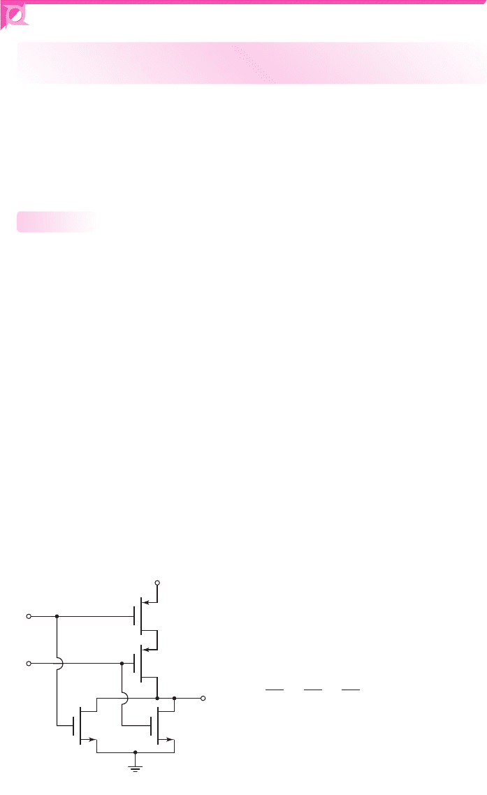
Basic CMOS NOR and NAND Gates
In the basic or classical CMOS logic circuits, the gates of a PMOS and an NMOS are
connected together, and additional PMOS and NMOS transistors are connected in se-
ries or parallel to form specific logic circuits. Figure 16.33(a) shows a two-input
CMOS NOR gate. The NMOS transistors are in parallel and the PMOS transistors
are in series.
If
A = B = logic 0
, then both
M
NA
and
M
NB
are cut off, and the current in the
circuit is zero. The source-to-gate voltage of
M
PA
is
V
DD
but the current is zero;
therefore,
v
SD
of
M
PA
is zero. This means that the source-to-gate voltage of
M
PB
is
also
V
DD
. However, since the current is zero, then
v
SD
of
M
PB
is also zero. The out-
put voltage is therefore
v
O
= V
DD
= logic 1
.
If the input signals are
A = logic 1 = V
DD
and
B = logic 0 = 0V
, then the
source-to-gate voltage of
M
PA
is zero, and the current in the circuit is again zero. The
gate-to-source voltage of
M
NA
is
V
DD
but the current is zero, so
v
DS
of
M
NA
is zero
and
v
O
= 0 = logic 0
. This result also holds for the other two possible input condi-
tions, since at least one PMOS is cut off and at least one NMOS is in a conducting
state. The NOR logic function is shown in the truth table of Figure 16.33(b).
16.4.1
v
O
M
NA
M
NB
A
V
DD
B
M
PB
M
PA
00
0
0
0
0
0
V
DD
V
DD
V
DD
V
DD
V
DD
v
O
AB
(a) (b)
Figure 16.33 (a) Two-input CMOS NOR logic circuit and (b) truth table
nea80644_ch16_1145-1254.qxd 07/12/2009 3:37 Page 1183 pinnacle MHDQ-New:MHDQ134:MHDQ134-16:
1184 Part 3 Digital Electronics
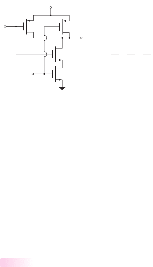
A two-input CMOS NAND logic gate is shown in Figure 16.34(a). In this case,
the NMOS transistors are in series and the PMOS transistors are in parallel. If
A = B = logic 0
, the two NMOS devices are cut off and the current in the circuit is
zero. The source-to-gate voltage of each PMOS device is
V
DD
, which means that
both PMOS transistors are in a conducting state. However, since the current is zero,
v
SD
for both
M
PA
and
M
PB
is zero and
v
O
= V
DD
. This result applies if at least one
input is a logic 0.
If the input signals are
A = B = logic 1 = V
DD
, then both PMOS transistors are
cut off, and the current in the circuit is zero. With
A = logic 1
,
M
NA
is in a conduct-
ing state; however, since the current is zero, then
v
DS
of
M
NA
is zero. This means that
the gate-to-source voltage of
M
NB
is also
V
DD
and
M
NB
is also in a conducting state.
However, since the current is zero, then
v
DS
of
M
NB
is zero, and
v
O
= logic 0 = 0V
.
The NAND logic function is shown in the truth table in Figure 16.34(b).
In both the CMOS NOR and NAND logic gates, the current in the circuit is
essentially zero when the inputs are in any quiescent state. Only very small reverse-
bias pn junction currents exist. The quiescent power dissipation is therefore essen-
tially zero. Again, this is the primary advantage of CMOS circuits.
Transistor Sizing
CMOS Inverter
We briefly discussed in Section 16.3.2 the sizing of transistors in the CMOS inverter
in terms of symmetrical transfer curves. Other factors involved in the sizing of tran-
sistors are, for example, switching speed, power, area, and noise margin.
Since the standby power is very small in a CMOS inverter, the sizing can be based
on switching speed. We will specify that the switching time in the pull-up mode
should be the same as the switching time in the pull-down mode. Figure 16.35(a)
shows the effective CMOS inverter in the pull-down mode. The PMOS is cutoff and
the load capacitance is discharged through the NMOS device. The switching time is
therefore a function of the current capability of the NMOS transistor. Figure 16.35(b)
shows the effective CMOS inverter in the pull-up mode. The NMOS is cutoff and the
16.4.2
v
O
B
A
M
PB
M
PA
V
DD
M
NA
M
NB
00
0
0
V
DD
V
DD
0
V
DD
V
DD
V
DD
V
DD
V
DD
v
O
AB
(a) (b)
Figure 16.34 (a) Two-input CMOS NAND logic circuit and (b) truth table
nea80644_ch16_1145-1254.qxd 07/12/2009 3:37 Page 1184 pinnacle MHDQ-New:MHDQ134:MHDQ134-16:
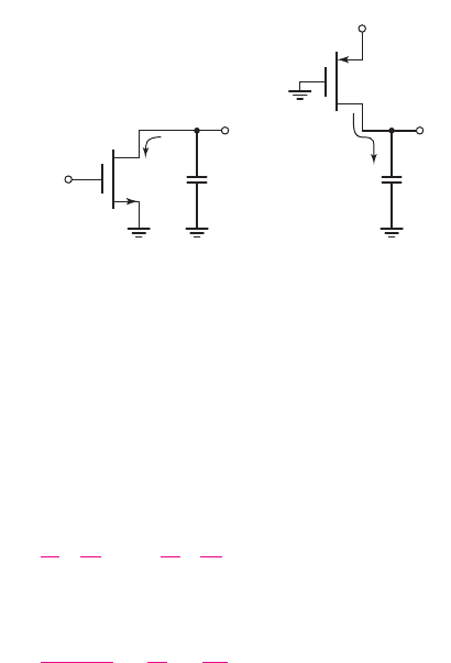
Chapter 16 MOSFET Digital Circuits 1185
load capacitance is charged through the PMOS device. The switching time is a func-
tion of the current capability of the PMOS transistor.
Assuming that
V
TN
=|V
TP
|
, equal switching times then implies that the con-
duction parameters of the NMOS and PMOS devices be equal, or
k
n
2
W
L
n
=
k
p
2
W
L
p
(16.68)
Assuming that
μ
n
≈ 2μ
p
, we have
(W/L)
p
(W/L)
n
=
k
n
k
p
=
μ
n
μ
p
≈ 2
(16.69)
The width-to-length ratio of the PMOS device must be approximately twice as large
as that of the NMOS device to obtain equal switching times.
In any given technology, the channel lengths of the NMOS and PMOS devices
are the same. Therefore the channel widths are sized to the desired value. We can
write that
W
n
= W
and
W
p
= 2W
, where
W
n
and
W
p
are the channel widths of the
NMOS and PMOS devices, respectively, and W is a standard width.
CMOS Logic Gates
We can now consider the sizing of transistors in the basic CMOS NAND and NOR
logic gates. We will specify, again, equal pull-up and pull-down switching times, and
we want the same switching times as the CMOS inverter with a load capacitance
C
L
.
We will use the effective 2:1 ratio between PMOS and NMOS sizes from the CMOS
inverter.
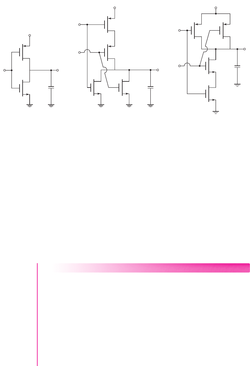
Consider the two-input CMOS NOR gate shown in Figure 16.33. Assume a load
capacitance
C
L
is connected to the output. In the worst case during a pull-down op-
eration, only one NMOS device will be turned on. To achieve the same switching
time as the CMOS inverter, the NMOS channel widths should be
W
n
= W
. If both
NMOS devices are turned on, the effective channel width will be doubled (see Fig-
ure 16.14(a)) and the switching time will be shorter.
During a pull-up operation, both PMOS devices must be turned on. Since the
PMOS devices are in series, the effective channel length doubles (see Figure 16. 14(b)).
Therefore, to maintain the same effective width-to-length ratio, the channel widths
must be doubled. We must therefore have
W
p
= 2(2W) = 4W
.
v
I
=
V
DD
C
L
V
DD
v
O
(a) (b)
C
L
v
O
Figure 16.35 (a) Effective CMOS inverter in pull-down mode and (b) effective CMOS
inverter in pull-up mode
nea80644_ch16_1145-1254.qxd 07/12/2009 3:37 Page 1185 pinnacle MHDQ-New:MHDQ134:MHDQ134-16:
1186 Part 3 Digital Electronics
Now consider the two-input NAND logic gate shown in Figure 16.34. Again, as-
sume a load capacitance
C
L
is connected to the output. In the worst case during a
pull-up operation, only one PMOS device will be turned on. This is equivalent to the
CMOS inverter, so the channel width should be
W
p
= 2W
. If both PMOS devices are
turned on, the effective channel width is doubled and the switching time will be
shorter.
During the pull-down operation, both NMOS devices must be turned on. Again,
since the NMOS devices are in series, the effective channel length doubles. There-
fore to maintain the same effective width-to-length ratio, the channel widths must be
doubled. We must therefore have
W
n
= 2(W) = 2W
.
The results of the transistor sizing for the CMOS inverter, and CMOS NOR and
NAND gates are shown in Figure 16.36.
EXAMPLE 16.10
Objective: Determine the transistor width-to-length ratios of a three-input CMOS
NAND logic gate.
Symmetrical switching times are desired and the switching times should corre-
spond to the basic CMOS inverter.
Solution: There are three p-channel transistors in parallel for the three-input CMOS
NAND gate. The worst case is when only one PMOS device is on in the pull-up
mode. This corresponds to the basic CMOS inverter, so the effective width should be
W
p
= 2W
.
There are three n-channel transistors in series for the three-input CMOS NAND
gate. All three transistors must be turned on in the pull-down mode. For three tran-
sistors in series, the effective channel length triples. Therefore, to keep the effective
NMOS width equal to W, we must have
W
n
= 3(W) = 3W
.
W
p
= 2W
W
p
= 4W
W
p
= 2W
W
p
= 2W
W
n
= 2W
W
n
= 2W
W
p
= 4W
W
n
= W
W
n
= W
W
n
= W
C
L
C
L
C
L
V
DD
V
DD
V
DD
F
F
F
A
A
B
A
B
(a) (b) (c)
Figure 16.36 The width-to-length ratios of (a) the CMOS inverter, (b) the CMOS NOR gate,
and (c) the CMOS NAND gate
nea80644_ch16_1145-1254.qxd 07/12/2009 3:37 Page 1186 pinnacle MHDQ-New:MHDQ134:MHDQ134-16:

Chapter 16 MOSFET Digital Circuits 1187
The results are shown in Figure 16.37.
Comment: As the number of inputs to a basic CMOS logic gate increases, the size
of the transistors must increase. The increased area of the transistors means that the
effective input capacitance increases so that switching times of cascaded logic gates
will increase.
EXERCISE PROBLEM
Ex 16.10: Determine the transistor sizes of a 3-input CMOS NOR logic gate.
Symmetrical switching times are desired and the switching times should corre-
spond to the basic CMOS inverter. (Ans.
W
p
= 6W
,
W
n
= W
)
Complex CMOS Logic Circuits
Just as with NMOS logic designs, we can form complex logic gates in CMOS, which
avoids connecting large numbers of NOR, NAND, and inverter gates to implement
the logic function. There are formal methods that can be used to implement the logic
circuit. However, we can use the knowledge gained in the analysis and design of the
NOR and NAND circuits.
DESIGN EXAMPLE 16.11
Objective: Design a CMOS logic circuit to implement a particular logic function.
Implement the logic function
Y = AB + C(D + E)
in a CMOS design. The
signals A, B, C, D, and E are available.
Design Approach: The general CMOS design is shown in Figure 16.38, in which
the inputs are applied to both the PMOS and NMOS networks. We may start the
16.4.3
C
L
W
p
=
2W
BAC
W
p
=
2W
A
W
n
= 3W
W
n
= 3W
W
n
= 3W
B
C
W
p
=
2W
V
DD
F
Figure 16.37 Width-to-length ratios for a three-input CMOS NAND logic gate
nea80644_ch16_1145-1254.qxd 07/12/2009 3:37 Page 1187 pinnacle MHDQ-New:MHDQ134:MHDQ134-16: