Neamen D. Microelectronics: Circuit Analysis and Design
Подождите немного. Документ загружается.

1198 Part 3 Digital Electronics
v
O
v
I
V
DD
= 3.3 V
M
L
f
M
D
M
N
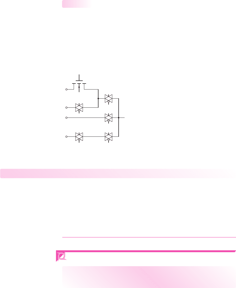
Figure 16.51 Figure for Exercise Ex16.13
EXERCISE PROBLEM
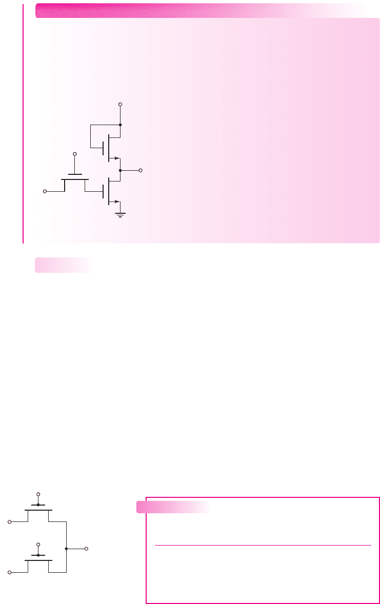
Ex 16.13: Consider the NMOS inverter with enhancement load driven by an
NMOS transmission gate in Figure 16.51. The threshold voltage of each n-channel
transistor is
V
TN
= 0.5
V. Neglect the body effect. Design
K
D
/K
L
of the inverter
such that
v
O
= 0.1
V when: (a)
v
I
= 2.8
V,
φ = 3.3
V; and (b)
v
I
= φ = 2.8
V.
(Ans. (a)
K
D
/K
L
= 16.2
,(b)
K
D
/K
L
= 20.8)
B
A
A
–
–
B
M
N1
M
N2
f
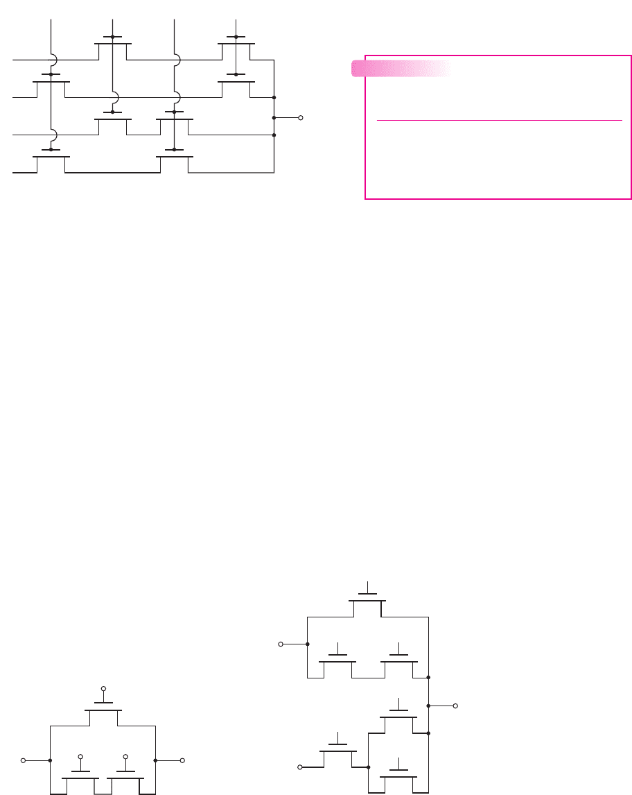
Figure 16.52 Simple NMOS
pass logic network
Table 16.1 Input and output states for the
circuit in Figure 16.52
State AB
¯
A
¯
BM
N1
M
N2
f
1 0011 off on 1
2 1001 off on 0
3 0110 on off 0
4 1100 on off 1
NMOS Pass Networks
As integrated circuit technology advances, one emphasis is on increased circuit den-
sity. The maximum number of circuit functions per unit area is determined either by
power dissipation density or by the area occupied by transistors and related devices.
One form of NMOS circuit logic that minimizes power dissipation and maximizes
device density is called pass transistor logic. Pass transistor circuits use minimum-
sized transistors, providing high density and high operating speed. The average power
dissipation is due only to the switching power consumed by the driver circuits in charg-
ing and discharging the pass transistor control gates and driving the pass network inputs.
In this section, we present a few examples of NMOS pass transistor logic cir-
cuits. Consider the circuit in Figure 16.52. To determine the output response, we ex-
amine the conditions listed in Table 16.1 for the possible states of the input signals A
and B. We assume that a logic 1 level is
V
DD
volts. In states 1 and 2, transmission
gate
M
N2
is biased in its conducting state. For state 1,
¯
A = logic 1
is transmitted to
the output so
f = logic 1
, where the logic
1
level is (
V
DD
− V
TN
). The logic 1 level
is attenuated by one threshold voltage drop. For state 2,
A = logic 0
is transmitted
16.6.2
nea80644_ch16_1145-1254.qxd 07/12/2009 3:38 Page 1198 pinnacle MHDQ-New:MHDQ134:MHDQ134-16:
Chapter 16 MOSFET Digital Circuits 1199
unattenuated to the output. In states 3 and 4, transmission gate
M
N1
is biased in its
conducting state. The
A = logic 0
for state 3 is transmitted unattenuated to the out-
put, and
A = logic 1
for state 4 is attenuated during transmission; therefore,
f =
logic 1
. The output is thus the exclusive-NOR function.
Another example of an NMOS pass transistor logic circuit is shown in Fig-
ure 16.53. The output response as a function of the input gate controls A and B is
shown in Table 16.2. This circuit is a multiplexer; that is, for a specific set of gate con-
trols, the input signals
P
i
are individually passed to the output. By using both normal
and inverted forms of A and B, four inputs can be controlled with just two variables.
A potential problem of NMOS pass transistor logic is that the output may be left
floating in a high impedance state and charged high. Consider the circuit shown in
Figure 16.54. If, for example,
¯
B = C = logic 0
and
A = logic 1
, then
f = logic 1
,
which is the logic 1 level attenuated by
V
TN
. When A is switched to logic 0, the out-
put should be low, but there may not be a discharge path to ground, and the output
may retain the logic 1
stored at the output capacitance.
The NMOS pass network must be designed to avoid a high impedance output by
passing a logic 0 whenever a 0 is required at the output. A logic network that per-
forms the logic function
f = A +
¯
B · C
, as indicated in Figure 16.54, is shown in
Figure 16.55. The complementary function
¯
f =
¯
A ·(B +
¯
C)
attached at the output
node drives the output to a logic 0 whenever
f = 0
.
A
f = A + B
⋅
C
C
V
DD
–
–
B
Figure 16.54 NMOS pass logic network with
a potential problem
BB
A
f
A
P
1
P
2
P
3
P
4
–
–
Figure 16.53 NMOS pass logic network example
A
f
C
O
V
DD
–
B
–
A
B
–
C
Figure 16.55 NMOS pass logic network
with complementary function in parallel
Table 16.2 Input and output states for
the circuit in Figure 16.53
State AB
¯
A
¯
Bf
10011P
1
21001P
2
30110P
3
41100P
4
nea80644_ch16_1145-1254.qxd 07/12/2009 3:38 Page 1199 pinnacle MHDQ-New:MHDQ134:MHDQ134-16:
1200 Part 3 Digital Electronics
ab
NMOS
PMOS
V
DD
v
O
C
L
v
I
dc
–
C
L
v
O
v
I
–
(a) (b)
f
f
f
f
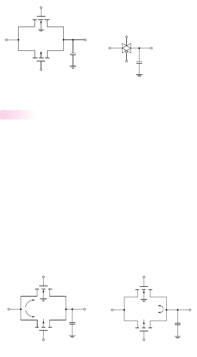
Figure 16.56 (a) CMOS transmission gate and (b) simplified circuit symbol
CMOS Transmission Gate
A CMOS transmission gate is shown in Figure 16.56(a). The parallel combination
of NMOS and PMOS transistors, with complementary gate signals, allows the input
signal to be transmitted to the output without the threshold voltage attenuation. Both
transistors must be bilateral; therefore, the NMOS substrate is connected to the most
negative potential in the circuit and the PMOS substrate is connected to the most pos-
itive potential (usually, ground and
V
DD
, respectively). Figure 16.56(b) shows a fre-
quently used simplified circuit symbol for the CMOS transmission gate.
We again assume that the transmission gate is to operate over a voltage range of
zero-to-
V
DD
. If the control voltages are
φ = 0
and
¯
φ = V
DD
, then both the NMOS
and PMOS transistors are cut off and the output is isolated from the input. In this
state, the circuit is essentially an open switch.
If
φ = V
DD
,
¯
φ = 0
,
v
I
= V
DD
, and
v
O
is initially zero, then for the NMOS de-
vice, terminal a acts as the drain and terminal b acts as the source, whereas for the
PMOS device, terminal c acts as the drain and terminal d acts as the source. Current
enters the NMOS drain and the PMOS source, as shown in Figure 16.57(a), to charge
the load capacitor. The NMOS gate-to-source voltage is
v
GSN
= φ − v
O
= V
DD
−v
O
(16.78(a))
16.6.3
(a) (b)
ab
dc
f = 0
NMOS
PMOS
V
DD
v
O
C
L
f = V
DD
v
I
= 0
–
+
+
–
–
v
SGP
v
GSN
i
DN
i
DP
ab
dc
NMOS
PMOS
V
DD
v
O
C
L
v
I
= V
DD
f = V
DD
f = 0
–
+
+
–
–
v
GSN
v
SGP
i
DN
i
DP
Figure 16.57 Currents and gate–source voltages in CMOS transmission gate for: (a) input
high condition and (b) input low condition
nea80644_ch16_1145-1254.qxd 07/12/2009 3:38 Page 1200 pinnacle MHDQ-New:MHDQ134:MHDQ134-16:
Chapter 16 MOSFET Digital Circuits 1201
n
v
O
v
I
C
L
p
p
NMOS
PMOS
p
n
n
f = V
DD
V
DD
f = 0
–
a
b
c
Figure 16.58 CMOS transmission gate showing cross sections of NMOS and
PMOS transistors
and the PMOS source-to-gate voltage is
v
SGP
= v
I
−
¯
φ = V
DD
−0 = V
DD
(16.78(b))
As with the NMOS transmission gate, when
v
O
= V
DD
− V
TN
, the NMOS transis-
tor cuts off and
i
DN
= 0
since
V
GSN
= V
TN
. However, since the source-to-gate volt-
age of the PMOS device is a constant at
v
SGP
= V
DD
, the PMOS transistor continues
to conduct. The drain current
i
DP
goes to zero when the PMOS source-to-drain volt-
age goes to zero, or
v
SDP
= 0
. This means that the load capacitor
C
L
continues to
charge through the PMOS device until the output and input voltages are equal, or in
this case,
v
O
= v
I
= V
DD
.
Consider what happens if
φ = V
DD
,
¯
φ = 0
,
v
I
= 0
, and
v
O
= V
DD
initially. For
the NMOS device, terminal a acts as the source and terminal b acts as the drain,
whereas for the PMOS device, terminal c acts as the source and terminal d acts as the
drain. Current enters the NMOS drain and the PMOS source, as shown in Figure
16.57(b), to discharge the capacitor. The NMOS gate-to-source voltage is
v
GSN
= φ − v
I
= V
DD
−0 = V
DD
(16.79(a))
and the PMOS source-to-gate voltage is
v
SGP
= v
O
−
¯
φ = v
O
−0 = v
O
(16.79(b))
When
v
SGP
= v
O
=|V
TP
|
, the PMOS device cuts off and
i
DP
goes to zero. How-
ever, since
v
GSN
= V
DD
, the NMOS transistor continues conducting and capacitor
C
L
completely discharges to zero.
Using a CMOS transmission gate in a MOS circuit may introduce a dynamic con-
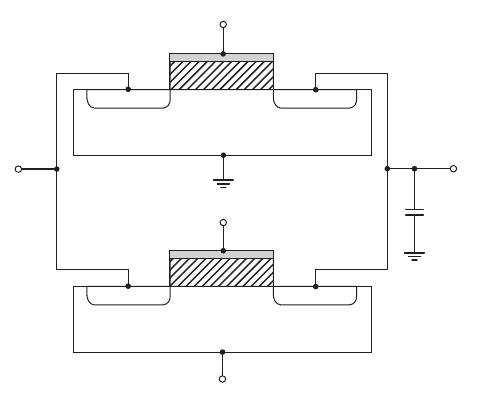
dition. Figure 16.58 shows the CMOS transmission gate with simplified cross sections
of the NMOS and PMOS transistors. If
φ = 0
and
¯
φ = V
DD
, then the input and output
are isolated. If
v
O
= V
DD
, then the NMOS substrate-to-terminal b pn junction is
reverse biased and capacitance
C
L
can discharge, as it did in the NMOS transmission
gate. If, however,
v
O
= 0
, then the PMOS terminal c-to-substrate pn junction is reverse
biased and capacitance
C
L
can charge to a positive voltage. This circuit is therefore
dynamic in that the output high or low conditions do not remain constant with time.
nea80644_ch16_1145-1254.qxd 07/12/2009 3:38 Page 1201 pinnacle MHDQ-New:MHDQ134:MHDQ134-16:
1202 Part 3 Digital Electronics
1
B
B
A
–
–
D
D
f
V
DD
PMOS
–
A
–
C
–
A
C
–
Figure 16.59 CMOS pass logic network
CMOS Pass Networks
CMOS transmission gates may also be used in pass network logic design. CMOS
pass networks use NMOS transistors to pass 0’s, PMOS transistors to pass 1’s, and
CMOS transmission gates to pass a variable to the output. An example is shown in
Figure 16.59. One PMOS transistor is used to transmit a logic 1, while transmis-
sion gates are used to transmit a variable that may be either a logic 1 or a logic 0. We
can show that for any combination of signals, a logic 1 or logic 0 is definitely passed
to the output.
16.6.4
Test Your Understanding
TYU 16.13 Design an NMOS pass network to perform the logic function
f = A(B + C)
.
TYU 16.14 Consider the CMOS transmission gate in Figure 16.56(a). Assume
transistor parameters of
V
TN
= 0.4
V and
V
TP
=−0.4
V. When
φ = 2.5
V, t h e
input voltage
v
I
varies with time as
v
I
= 2.5 −0.2t
for
0 ≤ t ≤ 12.5
s. Let
v
O
(t = 0) = 2.5
V and assume
C
L
= 0.2
pF. Determine the range of times that the
NMOS and PMOS devices are conducting. (Ans. NMOS conducting for
2 ≤ t ≤ 12.5
s; PMOS conducting for
0 ≤ t ≤ 10.5
s).
16.7 SEQUENTIAL LOGIC CIRCUITS
Objective: • Analyze and understand the characteristics of shift reg-
isters and various flip-flop designs.
In the logic circuits that we have considered in the previous sections, such as NOR and
NAND logic gates, the output is determined only by the instantaneous values of the
input signals. These circuits are therefore classified as combinational logic circuits.
nea80644_ch16_1145-1254.qxd 07/12/2009 3:38 Page 1202 pinnacle MHDQ-New:MHDQ134:MHDQ134-16:
Chapter 16 MOSFET Digital Circuits 1203
v
O4
v
I
f
1
f
2
V
DD
M
D2
v
O3
v
O2
V
DD
M
D1
v
O1
M
N1
M
N2
C
L2
C
L1
M
L2
M
L1
Figure 16.60 Dynamic shift register with NMOS inverters and transmission gates
Another class of circuits is called sequential logic circuits. The output depends
not only on the inputs, but also on the previous history of its inputs. This feature gives
sequential circuits the property of memory. Shift registers and flip-flops are typical
examples of such circuits. We will also briefly consider a full-adder circuit. The char-
acteristic of these circuits is that they store information for a short time until the
information is transferred to another part of the system.
In this section, we introduce a basic shift register and the basic concept of a flip-
flop. These circuits can become very complex and are usually described with logic
diagrams. We will also introduce a CMOS full adder circuit in terms of its logic
diagram and then provide the transistor implementation of this logic function. Addi-
tional information can be found in more advanced texts.
Dynamic Shift Registers
A shift register can be formed from transmission gates and inverters. Figure 16.60
shows a combination of NMOS transmission gates and NMOS depletion-load in-
verters. The clock signals applied to the gates of the NMOS transmission gates must
be complementary, nonoverlapping pulses. The effective capacitances at the gates of
M
D1
and
M
D2
are indicated by the dotted connections to
C
L1
and
C
L2
.
16.7.1
If, for example,
C
L1
is initially uncharged when
v
O1
= 0
and if
v
I
= V
DD
when
φ
1
= V
DD
, then a logic
1
= V
DD
− V
TN
voltage should exist at
v
O1
at the end of
clock pulse
φ
1
. The capacitance of
C
L1
charges through
M
N1
and the driving circuit
of
v
I
. The effective RC time constant must be sufficiently small to achieve this charg-
ing effect. As
v
O1
goes high,
v
O2
goes low, but the low is not transmitted through
M
N2
as long as
φ
2
remains low.
Figure 16.61 is used to determine the operation of this circuit and the voltages at
various times. For simplicity, we assume that
V
DD
= 5V
and
V
TN
= 1V
for the
NMOS drivers and transmission gate transistors.
At
t = t
1
,
v
I
= φ
1
= 5
V,
v
O1
charges to
v
DD
− V
TN
= 4
V, and
v
O2
goes low. At
this time,
M
N2
is still cut off, which means that the values of
v
O3
and
v
O4
depend on
the previous history. At
t = t
2
,
φ
1
is zero,
M
N1
is cut off, but
v
O1
remains charged. At
t = t
3
,
φ
2
is high, and the logic 0 at
v
O2
is transmitted to
v
O3
, which forces
v
O4
to 5 V.
The input signal
v
I
= 5V
at
t = t
1
has thus been transmitted to the output; therefore,
nea80644_ch16_1145-1254.qxd 07/12/2009 3:38 Page 1203 pinnacle MHDQ-New:MHDQ134:MHDQ134-16:
1204 Part 3 Digital Electronics
v
O4
= v
I
= 5V
at
t = t
3
. The input signal is transmitted, or shifted, from the input to
the output during one clock cycle, making this circuit one stage of a shift register.
At
t = t
4
,
v
I
= 0
, and
φ
1
= 5
V, so that
v
O1
= 0
and
v
O2
= 5V
. Since
φ
2
= 0
,
M
N2
is cut off, and
v
O2
and
v
O3
are isolated. At
t = t
5
,
φ
2
= 5
V, so that
v
O3
charges
to
V
DD
− V
TN
= 4
V, and
v
O4
goes low (logic 0). At
t = t
6
, both NMOS transmis-
sion gates are cut off, and the two inverters remain in their previous states. It is im-
portant that
φ
1
and
φ
2
do not overlap, or the signal would propagate through the
whole chain at once and we would no longer have a shift register.
In the dynamic condition of NMOS transmission gates, the high output voltage
across the output capacitance does not remain constant with time; it discharges
through the transmission gate transistor. This same effect applies to the shift register
in Figure 16.60. For example, from Figure 16.61, at
t = t
2
,
v
O1
= 4V
,
φ
1
= 0
, and
M
N1
is cut off. Voltage
v
O1
will start to decay and
v
O2
will begin to increase. To pre-
vent logic errors from being introduced into the system, the clock signal period T
must be small compared to the effective RC discharge time constant. The circuit in
Figure 16.60 is therefore called a dynamic shift register.
A dynamic shift register formed in a CMOS technology is shown in Figure 16.62.
Operation of this circuit is very similar to that of the dynamic NMOS shift register,
except for the voltage levels. For example, when
v
I
= φ
1
= V
DD
, then
v
O1
= V
DD
and
v
O2
= 0
. When
φ
2
goes high, then
v
O3
goes to zero,
v
O4
= V
DD
, and the input
signal is shifted to the output during one clock period.
V
DD
v
O4
f
1
f
2
v
I
v
O3
v
O2
v
O1
V
DD
Figure 16.62 CMOS dynamic shift register
v
O4
Time
t
1
t
2
t
4
t
5
t
6
t
3
0
5
v
O3
0
5
4
4
v
O2
0
5
v
O1
0
5
v
I
0
5
0
5
0
5
f
1
f
2
TT
Figure 16.61 NMOS shift register voltages at various times
nea80644_ch16_1145-1254.qxd 07/12/2009 3:38 Page 1204 pinnacle MHDQ-New:MHDQ134:MHDQ134-16:
Chapter 16 MOSFET Digital Circuits 1205
R
S
V
DD
QQ
–
M
1
M
4
M
2
M
5
M
6
M
3
Figure 16.63 NMOS R–S flip-flop
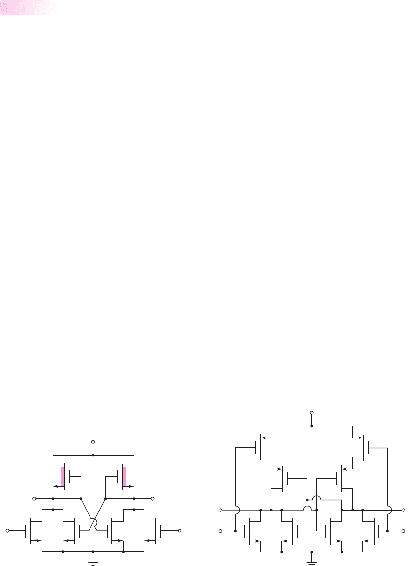
R–S Flip-Flop
Flip-flops are bistable circuits usually formed by cross-coupling two NOR gates.
Figure 16.63 shows an R–S flip-flop using NMOS NOR logic gates with depletion
loads. As shown,
M
1
,
M
2
, and
M
3
form one NOR gate, and
M
4
,
M
5
, and
M
6
form the
second. The outputs of the two NOR circuits are connected back to the inputs of the
opposite NOR gates.
If we assume that
S = logic 1
and
R = logic 0
, then
M
1
is biased in its con-
ducting state and output
¯
Q
is forced low. The inputs to both
M
4
and
M
5
are low, so
output Q goes high to a
logic 1 = V
DD
. Transistor
M
2
is then also biased in a con-
ducting state. The two outputs Q and
¯
Q
are complementary and, by definition, the
flip-flop is in the set state when
Q = logic 1
and
¯
Q = logic 0
.
If S returns to logic 0, then
M
1
turns off, but
M
2
remains turned on so
¯
Q
remains
low and Q remains high. Therefore, when S goes low, nothing in the circuit can force
a change and the flip-flop stores this particular logic state.
When
R = logic 1
and
S = logic 0
, then
M
4
turns on so output Q goes low.
With
S = Q = logic 0
, then both
M
1
and
M
2
are cut off and
¯
Q
goes high. Transistor
M
5
turns on, keeping Q low when R goes low. The flip-flop is now in the reset state.
If both S and R inputs were to go high, then both outputs Q and
¯
Q
would go low.
However, this would mean that the outputs would not be complementary. Therefore,
a logic 1 at both S and R is considered to be a forbidden or nonallowed condition. If
both inputs go high and then return to logic 0, the state of the flip-flop is determined
by whichever input goes low last. If both inputs go low simultaneously, then the out-
puts will flip into one state or the other, as determined by slight imbalances in tran-
sistor characteristics.
Figure 16.64 shows an R–S flip-flop using CMOS NOR logic gates. The outputs
of the two NOR gates are connected back to the inputs of the opposite NOR gates to
form the flip-flop.
If
S = logic 1
and
R = logic 0
, then
M
N1
is turned on,
M
P1
is cut off, and
¯
Q
goes
low. With
¯
Q = R = logic 0
, then both
M
N3
and
M
N4
are cut off, both
M
P3
and
M
P4
are biased in a conducting state so that the output Q goes high. With
Q = logic 1
,
M
N2
is biased on,
M
P2
is biased off, and the flip-flop is in a set condition. When S goes low,
M
N1
turns off,
M
N2
remains conducting, so the state of the flip-flop does not change.
16.7.2
R
S
Q
V
DD
Q
–
M
N1
M
N2
M
N4
M
N3
M
P3
M
P1
M
P4
M
P2
Figure 16.64 CMOS R–S flip-flop
nea80644_ch16_1145-1254.qxd 07/12/2009 3:38 Page 1205 pinnacle MHDQ-New:MHDQ134:MHDQ134-16:

1206 Part 3 Digital Electronics
When
S = logic 0
and
R = logic 1
, then output Q is forced low, output
¯
Q
goes
high, and the flip-flop is in a reset condition. Again, a logic 1 at both S and R is con-
sidered to be a forbidden or a nonallowed condition, since the resulting outputs are
not complementary.
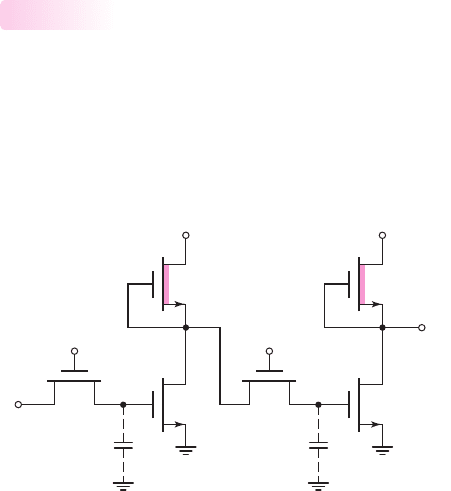
D Flip-Flop
A D-type flip-flop is used to provide a delay. The logic bit on the D input is trans-
ferred to the output at the next clock pulse. This flip-flop is used in counters and shift
registers. The basic circuit is similar to the CMOS dynamic shift register in Fig-
ure 16.62, except that additional circuitry makes the D flip-flop a static circuit.
Consider the circuit in Figure 16.65. The CMOS inverter composed of
M
N2
and
M
P2
is driven by a CMOS transmission gate composed of
M
N1
and
M
P1
. A second
CMOS inverter,
M
N3
and
M
P3
, is connected in a feedback configuration. If
v
I
=
high, then
v
O1
goes high when the transmission gate is conducting, and output
v
O
,
which is the input to the feedback inverter, goes low.
When the CMOS transmission gate turns off, the pn junction in the
M
N1
trans-
mission gate transistor is reverse biased. In this case, however, voltage
v
O1
is not sim-
ply across the gate capacitance of inverter
M
N2
–M
P2
. Transistor
M
P3
is biased in a
conducting state, so the reverse-biased pn junction leakage current
I
L
is supplied
through
M
P3
, as indicated in Figure 16.65. Since this leakage current is small, the
source-to-drain voltage of
M
P3
will be small, and
v
O1
will remain biased at essen-
tially
V
DD
. The circuit will therefore remain in this static condition.
Similarly, when
v
O1
is low and
v
O
is high, the pn junction in the
M
P1
transmis-
sion gate transistor is reverse biased and transistor
M
N3
is biased on. Transistor
M
N3
sinks the pn junction leakage current
I
L
, and the circuit remains in this static condi-
tion until changed by a new input signal through the transmission gate.
16.7.3
n
p
p
p
n
n
V
DD
V
DD
v
O
= Low
M
P2
M
P1
M
N1
v
O1
= High
v
I
= High
M
N2
V
DD
M
N3
M
P3
I
L
I
L
′
I
L
′
I
L
f
f
–
Figure 16.65 CMOS D-type flip-flop
nea80644_ch16_1145-1254.qxd 07/12/2009 3:38 Page 1206 pinnacle MHDQ-New:MHDQ134:MHDQ134-16:
Chapter 16 MOSFET Digital Circuits 1207
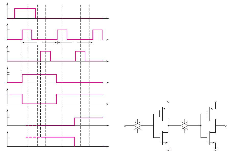
D
Q
Q′
TG2
TG3 TG4
TG1
Master Slave
ff
–
f
–
f
Figure 16.66 CMOS master–slave D flip-flop
D
Q ′
f
Q
Figure 16.67 D flip-flop signals at various times
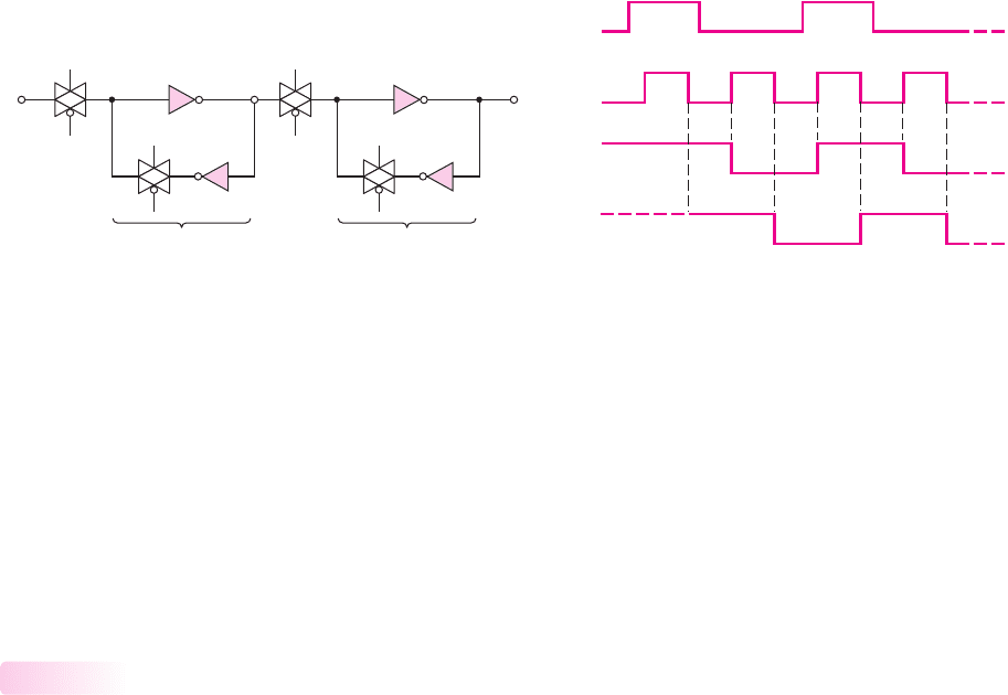
The circuit shown in Figure 16.66 is a master–slave configuration of a D flip-
flop. When clock pulse
φ
is high, transmission gate TG1 is conducting, and data D
goes through the first inverter, which means that
Q
=
¯
D
. Transmission gate TG2 is
off, so data stops at
Q
. When clock pulse
φ
goes low, then TG3 turns on, and the
master portion of the flip-flip is in a static configuration. Also when
φ
goes low, TG2
turns on, the data are transmitted through the slave portion of the flip-flop, and the
output is
Q =
¯
Q
= D
. The data present when
φ
is high are transferred to the output
of the flip-flop during the negative transition of the clock pulse. The various signals
in the D flip-flop are shown in Figure 16.67.
Additional circuitry can be added to the D flip-flop in Figure 16.66 to provide a
set and reset capability.
CMOS Full-Adder Circuit
One of the most widely used building blocks in arithmetic processing architectures
is the one-bit full-adder circuit. We will first consider the logic diagram from the
Boolean function and then consider the implementation in a conventional CMOS
design.
Assuming that we have two input bits to be added plus a carry signal from a pre-
vious stage, the sum-out and carry-out signals are defined by the following two
Boolean functions of three input variables A, B, and C.
Sum-out = A ⊕ B ⊕C
= ABC + A
¯
B
¯
C +
¯
A
¯
BC +
¯
AB
¯
C
(16.80(a))
Carry-out = AB + AC + BC
(16.80(b))
The logic diagrams for these functions are shown in Figure 16.68. As we have seen
previously, the implementation at the transistor level can be done with fewer transis-
tors than would be used if all the NOR and NAND gates were actually connected as
shown in the logic diagram.
Figure 16.69 is a transistor-level schematic of the one-bit full-adder circuit im-
plemented in a conventional CMOS technology. We can understand the basic design
from the logic diagram. For example, we may consider the NMOS portion of the
carry-out signal. We see that transistors
M
NA1
and
M
NB1
are in parallel, to perform
the basic OR function, and these transistors are in series with transistor
M
NC1
, to per-
form the basic AND function. These three transistors form the NMOS portion of the
design of the two gates labeled
G
1
and
G
2
in Figure 16.68. We also have transistors
M
NA2
and
M
NB2
in series, to perform the basic AND function of gate
G
3
. This set of
16.7.4
nea80644_ch16_1145-1254.qxd 07/12/2009 3:38 Page 1207 pinnacle MHDQ-New:MHDQ134:MHDQ134-16: