Neamen D. Microelectronics: Circuit Analysis and Design
Подождите немного. Документ загружается.


1158 Part 3 Digital Electronics
i
D
= 0
, the drain-to-source voltage of the load transistor must be zero; therefore,
v
O
= V
DD
for
v
I
≤ V
TND
. An advantage of the depletion-load inverter over the
enhancement-load inverter is that the high output voltage, or the logic 1 level, is at
the full
V
DD
value.
As the input voltage becomes just greater than the driver threshold voltage
V
TND
, the driver turns on and is biased in the saturation region; however, the load is
biased in the nonsaturation region. The Q-point lies between points A and B on the
load curve shown in Figure 16.7(c). We again set the two drain currents equal, or
i
DD
= i
DL
, which means that
K
D
[v
GSD
− V
TND
]
2
= K
L
2(v
GSL
− V
TNL
)v
DSL
−v
2
DSL
(16.22)
Writing Equation (16.22) in terms of the input and output voltages yields
K
D
[v
I
− V
TND
]
2
= K
L
[2(−V
TNL
)(V
DD
−v
O
) − (V
DD
−v
O
)
2
]
(16.23)
This equation relates the input and output voltages as long as the driver is biased in
the saturation region and the load is biased in the nonsaturation region.
There are two transition points for the NMOS inverter with a depletion load:
one for the load and one for the driver. These are points B and C, respectively, in
Figure 16.7(c). The transition point for the load is given by
v
DSL
= V
DD
− V
Ot
= v
GSL
− V
TNL
=−V
TNL
(16.24(a))
or
V
Ot
= V
DD
+ V
TNL
(16.24(b))
Since
V
TNL
is negative, the output voltage at the transition point is less than
V
DD
.
The transition point for the driver is given by
v
DSD
= v
GSD
− V
TND
or
V
Ot
= V
It
− V
TND
(16.25)
When the Q-point lies between points B and C on the load curve, both devices
are biased in the saturation region, and
K
D
(v
GSD
− V
TND
)
2
= K
L
(v
GSL
− V
TNL
)
2
(16.26(a))
or
K
D
K
L
(v
I
− V
TND
) =−V
TNL
(16.26(b))
Equation (16.26(b)) demonstrates that the input voltage is a constant as the Q-point
passes through this region. This effect is also shown in Figure 16.7(c); the load curve
between points B and C lies on a constant
v
GSD
curve. (This characteristic will
change when the body effect is taken into account.)
For an input voltage greater than the value given by Equation (16.26(b)), the dri-
ver is biased in the nonsaturation region while the load is biased in the saturation re-
gion. The Q-point is now between points C and D on the load curve in Figure 16.7(c).
Equating the two drain currents, we obtain
K
D
2(v
GSD
− V
TND
)v
DSD
−v
2
DSD
= K
L
(v
GSL
− V
TNL
)
2
(16.27(a))
which becomes
K
D
K
L
2(v
I
− V
TND
)v
O
−v
2
O
= (−V
TNL
)
2
(16.27(b))
nea80644_ch16_1145-1254.qxd 07/12/2009 3:37 Page 1158 pinnacle MHDQ-New:MHDQ134:MHDQ134-16:
Chapter 16 MOSFET Digital Circuits 1159
This equation implies that the relationship between the input and output voltages are
not linear in this region.
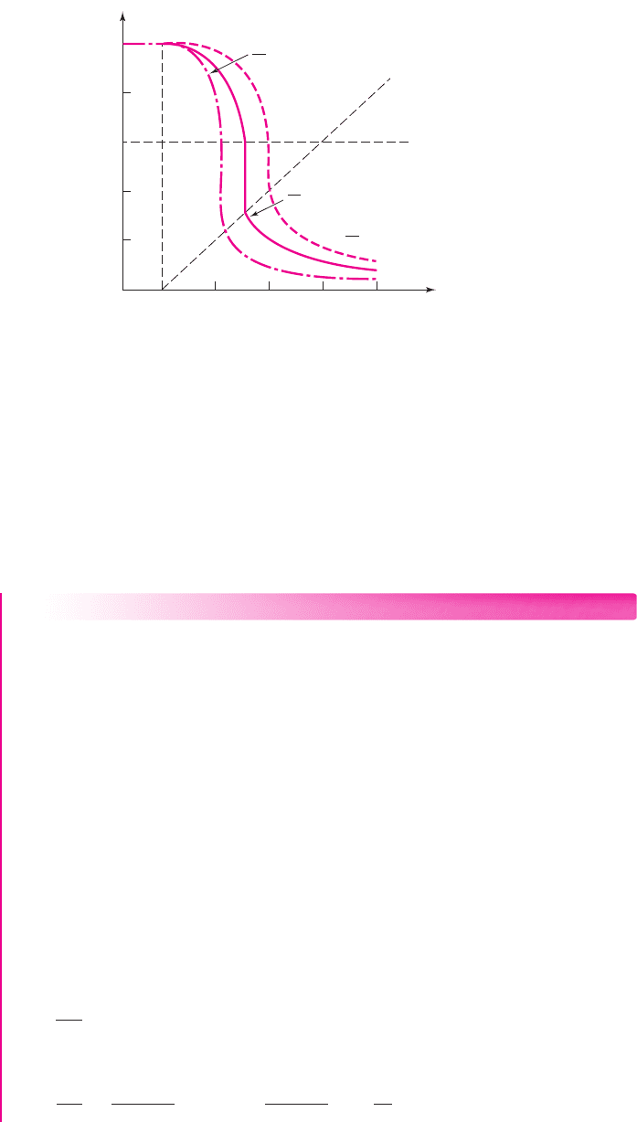
Figure 16.8 shows the voltage transfer characteristics of this inverter for three
values of
K
D
/K
L
. Also shown are the loci of transition points for the load and driver
transistors as given by Equations (16.24(b)) and (16.25), respectively.
DESIGN EXAMPLE 16.3
Objective: Design an NMOS inverter to meet a set of specifications and determine
the power dissipation in the inverter.
Specifications: The NMOS inverter with depletion load shown in Figure 16.7(a) is
to be designed such that
v
O
= V
OL
= 0.10
V when
v
I
= 2.5
V. The circuit is biased
at
V
DD
= 2.5
V. (Neglect the body effect.)
Choices: Transistors are available with process conduction parameters of
k
n
= 100 μ
A/V
2
. The driver transistor threshold voltage is
V
TND
= 0.5
V and the
load transistor threshold voltage is
V
TNL
=−1
V.
Solution: For
v
I
= 2.5
V, the driver transistor is biased in the nonsaturation region
and the load transistor is biased in the saturation region. Using Equation (16.27(b),
we find
K
D
[2(2.5 − 0.5)(0.1) − (0.1)
2
] = K
L
[0 − (−1)]
2
which yields
K
D
K
L
= 2.56
If we choose
(W/L)
L
= 1
, then
K
D
K
L
=
(W/L)
D
(W/L)
L
⇒ 2.56 =
(W/L)
D
1
⇒
W
L
D
= 2.56
v
O
(V)
V
DD
+ V
TNL
=
v
I (V)
1.0 2.0 2.50.5 1.5
0.5
1.0
1.5
2.0
2.5
0
Locus of transition
points, for load
Locus of transition
points, for driver
= 1
K
D
K
L
= 1.5
K
D
K
L
= 2.56
K
D
K
L
Figure 16.8 Voltage transfer characteristics of an NMOS inverter with depletion load, using
parameters from Example 16.3 and for three aspect ratios
nea80644_ch16_1145-1254.qxd 07/12/2009 3:37 Page 1159 pinnacle MHDQ-New:MHDQ134:MHDQ134-16:
1160 Part 3 Digital Electronics
The maximum current in the inverter occurs when the output is in its low state,
so, from the load transistor, we find
i
D,max
=
k
n
2
·
W
L
L
(0 − V
TNL
)
2
=
100
2
(1)[0 − (−1)]
2
= 50 μA
The maximum power dissipation in the inverter is
P
D,max
= i
D,max
· V
DD
= (50)(2.5) = 125 μW
Comment: A relatively low output voltage
V
OL
can be produced in the NMOS
inverter with depletion load, even when the load and driver transistors are not vastly
different in size. The power dissipation in this inverter is also substantially less than
in the enhancement-load inverter since the aspect ratio is smaller.
Design Consideration: The static analysis of the three types of NMOS inverters
clearly demonstrates the advantage of the depletion load inverter. The size of the dri-
ver transistor is smaller for a given load device size to produce a given low output
state. This allows a greater number of inverters to be fabricated in a given chip area.
In addition, since the power dissipation is less, more inverters can be fabricated on a
chip for a given total power dissipation.
EXERCISE PROBLEM
Ex 16.3: The depletion-load NMOS inverter shown in Figure 16.7(a) is biased at
V
DD
= 3
V. The transistor parameters are
k
n
= 100 μ
A/V
2
,
V
TND
= 0.4
V,
V
TNL
=−0.8
V,
(W/L)
D
= 6
, and
(W/L)
L
= 2
. (a) Determine
v
O
for
v
I
= 3
V.
Neglect the body effect. (b) Determine the maximum current and maximum power
dissipation in the inverter. (c) Find the transition points for the driver and load tran-
sistors. (Ans. (a)
v
O
= 0.0414
V; (b)
i
D,max
= 0.064
mA,
P
D,max
= 0.192
mW;
(c) driver:
V
It
= 0.862
V,
V
Ot
= 0.462
V; load:
V
It
= 0.862
V,
V
Ot
= 2.2
V)
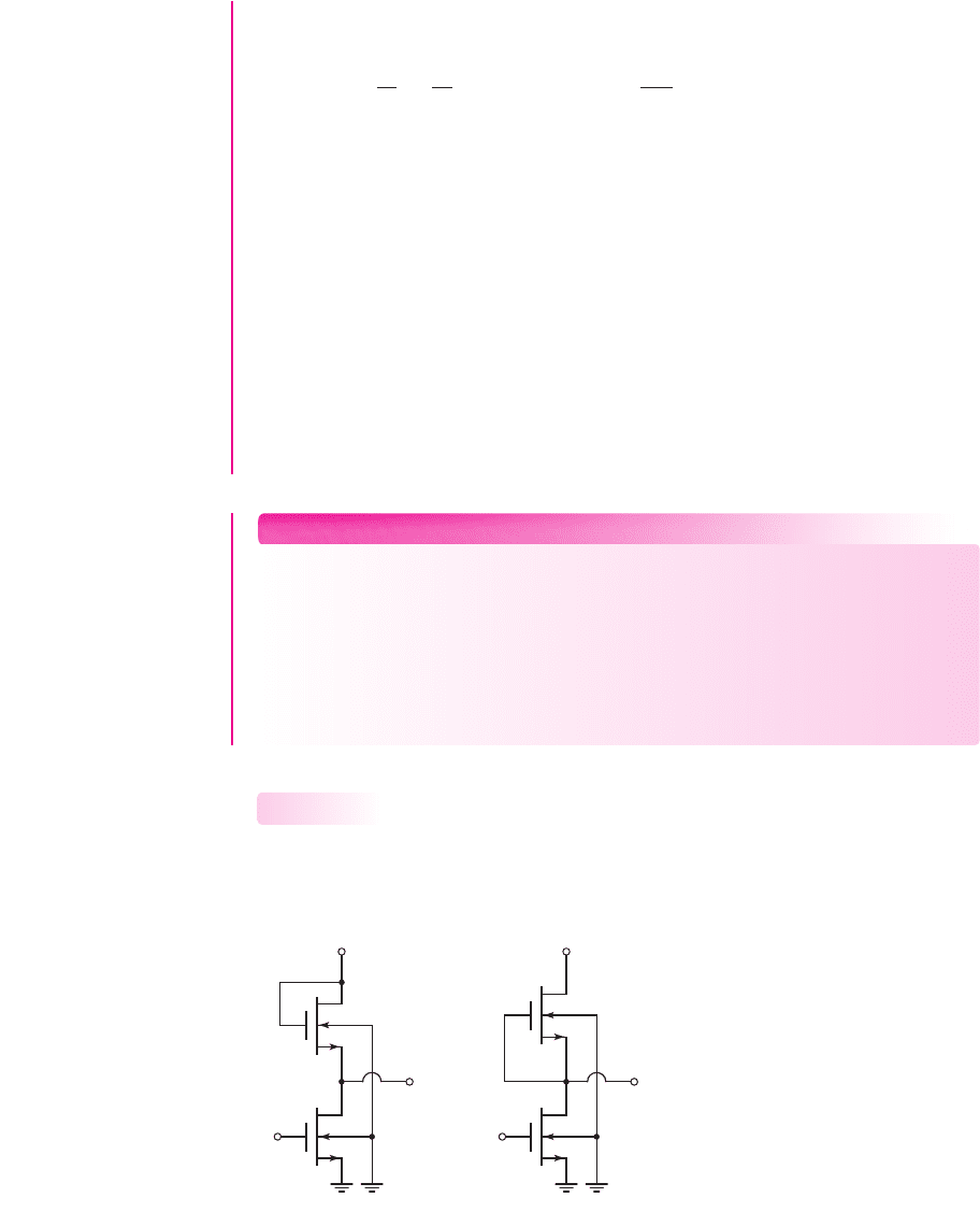
Body Effect
Up to this point, we have neglected the body effect and assumed that all threshold
voltages are constant. Figure 16.9 shows enhancement-load and depletion-load
16.1.3
V
DD
= 2.5 V
v
O
v
I
V
DD
= 2.5 V
v
O
v
I
(a) (b)
Figure 16.9 NMOS inverters, showing substrate connections to ground potential:
(a) enhancement-load inverter and (b) depletion-load inverter
nea80644_ch16_1145-1254.qxd 07/12/2009 3:37 Page 1160 pinnacle MHDQ-New:MHDQ134:MHDQ134-16:

Chapter 16 MOSFET Digital Circuits 1161
NMOS inverters with the substrates of all transistors tied to ground. A nonzero
source-to-body voltage will then exist in the load devices. In fact, the source terminal
of the depletion load can increase to
V
DD
. The threshold voltage equation, including
the body effect, must be used in the circuit calculations for the load transistor. This
significantly complicates the equations for the voltage transfer calculations, making
them very cumbersome for hand analyses.
EXAMPLE 16.4
Objective: Determine the change in the high output voltage of an NMOS inverter
with enhancement load, taking the body effect into account.
Consider the NMOS inverter with enhancement load in Figure 16.9(a). The tran-
sistor parameters are
V
TNDO
= V
TNLO
= 0.5
V and
K
D
/K
L
= 16
. Assume the in-
verter is biased at
V
DD
= 2.5
V, assume the body effect coefficient is
γ = 0.5
V
1/2
,
and let
φ
fp
= 0.365
V.
Solution: When
v
I
< V
TNDO
, the driver is cut off and the output goes high. From
Equation (16.14(b)), the maximum output voltage is
v
O,max
= V
OH
= V
DD
− V
TNL
where
V
TNL
is given by
V
TNL
= V
TNLO
+γ
2φ
fp
+ V
SB
−
2φ
fp
From Figure 16.9(a), we see that
V
SB
= v
O
. Therefore, Equation (16.14(b)) can
be written as
v
O,max
= V
DD
−
V
TNLO
+γ
2φ
fp
+v
O,max
−
2φ
fp
Defining
v
O,max
≡ V
OH
, we have
V
OH
−2.427 =−0.5
0.73 + V
OH
Squaring both sides and rearranging terms yields
V
2
OH
−5.1044V
OH
+5.7088 = 0
Consequently, the maximum output voltage, or the logic 1 level, is
V
OH
= 1.655 V
Comment: Neglecting the body effect, the logic 1 output level is
V
OH
= V
DD
− V
TNLO
= 2.5 −0.5 = 2.0V
The body effect, then, can significantly influence the logic high state of the NMOS
inverter with enhancement load. These results also impact the inverter noise margins.
The source and body terminals of the depletion load device in the NMOS in-
verter shown in Figure 16.9(b) are not at the same potential when the output goes
high. However, when the driver is cut off, the drain-to-source voltage of the depletion
device must be zero in order that
v
O,max
= V
OH
= V
DD
.
Computer Simulation: A computer analysis of the inverters in Figure 16.9 was
performed, neglecting the body effect and taking the body effect into account. The
parameters are
V
DD
= 5
V,
V
TNDO
= 0.8
V for the driver transistors,
V
TNLO
= 0.8
V
nea80644_ch16_1145-1254.qxd 07/12/2009 3:37 Page 1161 pinnacle MHDQ-New:MHDQ134:MHDQ134-16:
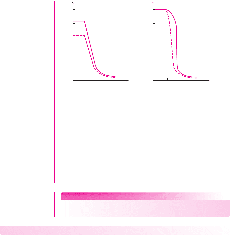
1162 Part 3 Digital Electronics
for the saturated load transistor, and
V
TNLO
=−2
V for the depletion load transistor.
The body effect coefficient was assumed to be
γ = 0.9
V
1/2
.
The body effect changes the voltage transfer characteristics of both the enhance-
ment load and depletion load inverters. Figure 16.10(a) shows the voltage transfer
characteristics for the enhancement load inverter. For
v
I
= 0
, the output voltage is
3.15
V when the body effect is taken into account. This compares to 4.2 V when the
body effect is neglected.
Figure 16.10(b) shows the voltage transfer characteristics for the depletion load
inverter. The output voltage is 5 V in the high state, which is independent of the body
effect. However, the characteristics during the transition region are a function of the
body effect.
EXERCISE PROBLEM
Ex 16.4: Repeat Example 16.4 for the case when the body effect coefficient is
γ = 0.3
V
1/2
. (Ans.
V
OH
= 1.781
V)
Test Your Understanding
TYU 16.1 Consider the NMOS inverter with enhancement load, as shown in Figure
16.5(a), biased at
V
DD
= 1.8
V. The threshold voltages are
V
TND
= V
TNL
= 0.4
V.
Assume
k
n
= 100 μ
A/V
2
. Design the width-to-length ratios such that the output
voltage is 0.12 V and the maximum inverter power dissipation is 0.50 mW when
v
I
= 1.4
V. Neglect the body effect. (Ans.
(W/L)
L
= 3.39
,
(W/L)
D
= 24.6)
TYU 16.2 Consider the depletion load inverter in Figure 16.7(a) biased at
V
DD
= 1.8
V. The threshold voltages are
V
TND
= 0.4
V and
V
TNL
=−0.6
V. Assume
k
n
= 100 μ
A/V
2
. Design the inverter such that the maximum inverter power dissipa-
tion is 0.2 mW and the output voltage is 0.08 V when
v
I
= 1.8
V. Neglect the body
effect. (Ans.
(W/L)
L
= 6.17
,
(W/L)
D
= 10.2)
v
O
(V)
v
I
(V)
1230
1
2
3
4
5
Neglecting
body effect
With
body effect
v
O
(V)
v
I
(V)
1230
1
2
3
4
5
Neglecting
body effect
With
body
effect
(a) (b)
Figure 16.10 Voltage transfer characteristics of NMOS inverters with and without the body
effect (a) enhancement load and (b) depletion load
nea80644_ch16_1145-1254.qxd 07/12/2009 3:37 Page 1162 pinnacle MHDQ-New:MHDQ134:MHDQ134-16:
Chapter 16 MOSFET Digital Circuits 1163
TYU 16.3 (a) Consider the results of Exercise Ex 16.1. Assume 100,000 resistor-
load inverters are fabricated on a single chip and the input voltage of each inverter is
high. Determine the current that must be supplied to each chip and the maximum
power that will be dissipated on each chip. (b) Repeat part (a) for Exercise Ex 16.2
and the enhancement-load inverter. (c) Repeat part (a) for Exercise Ex 16.3 and
the depletion-load inverter. (Ans. (a)
I = 9.8
A,
P = 29.4
W; (b)
I = 58.9
A,
P = 176.6
W; (c)
I = 6.4
A,
P = 19.2
W)
16.2 NMOS LOGIC CIRCUITS
Objective: • Analyze and design NMOS logic gates.
NMOS logic circuits are formed by combining driver transistors in parallel, series, or
series–parallel combinations to produce a desired output logic function.
NMOS NOR and NAND Gates
The NMOS NOR logic gate contains additional driver transistors connected in
parallel. Figure 16.11 shows a two-input NMOS NOR logic gate with a depletion
load. If
A = B = logic 0
, then both
M
DA
and
M
DB
are cut off and
v
O
= V
DD
. If
A = logic 1
and
B = logic 0
, then
M
DB
is cut off and the NMOS inverter configura-
tion with
M
L
and
M
DA
is the same as previously considered, and the output voltage
goes low. Similarly, if
A = logic 0
and
B = logic 1
, we again have the same inverter
configuration.
If
A = B = logic 1
, then both
M
DA
and
M
DB
turn on and the two driver tran-
sistors are effectively in parallel. The value of the output voltage now changes
slightly. Figure 16.12 shows the NOR gate when both input voltages are a logic 1.
From our previous analysis, we can assume that the two driver transistors are biased
16.2.1
A
v
O
V
DD
B
M
DA
M
DB
M
L
Figure 16.11 Two-input NMOS
NOR logic gate with depletion load
A = 2.5 V B = 2.5 V
v
O
V
DD
= 2.5 V
M
DA
M
DB
i
DL
i
DB
i
DA
+
–
v
GSA
+
–
v
GSB
M
L
Figure 16.12 Two-input NMOS NOR
logic gate for Example 16.5
nea80644_ch16_1145-1254.qxd 07/12/2009 3:37 Page 1163 pinnacle MHDQ-New:MHDQ134:MHDQ134-16:

1164 Part 3 Digital Electronics
in the nonsaturation region and the load device is biased in the saturation region.
We then have
i
DL
= i
DA
+i
DB
which in general terms can be written
K
L
[v
GSL
− V
TNL
]
2
= K
DA
2(v
GSA
− V
TNA
)v
DSA
−v
2
DSA
+ K
DB
2(v
GSB
− V
TNB
)v
DSB
−v
2
DSB
(16.28)
If we assume the two driver transistors are identical, then the driver conduction
parameters and threshold voltages are also identical, or
K
DA
= K
DB
≡ K
D
and
V
TNA
= V
TNB
≡ V
TND
. Noting that
v
GSL
= 0
,
v
GSA
= v
GSB
= V
DD
, and
v
DSA
=
v
DSB
= v
O
, we can write Equation (16.28) as
[−V
TNL
]
2
= 2
K
D
K
L
2(V
DD
− V
TND
)v
O
−v
2
O
(16.29)
Equation (16.29) shows that when both drivers are conducting, the effective
width-to-length ratio of the composite driver transistor doubles. This means that the
output voltage becomes slightly smaller when both inputs are high.
EXAMPLE 16.5
Objective: Determine the low output voltage of an NMOS NOR circuit.
Consider the NOR logic circuit in Figure 16.12 biased at
V
DD
= 2.5
V. Assume
transistor parameters of
k
n
= 100 μ
A/V
2
,
V
TND
= 0.4
V,
V
TNL
=−0.6
V,
(W/L)
D
= 4
, and
(W/L)
L
= 1
. Neglect the body effect.
Solution: If, for example,
A =
logic 1
= 2.5
V and
B =
logic 0, then
M
DA
is biased
in the nonsaturation region and
M
DB
is cut off. The output voltage is determined
from Equation (16.27(b)), which is
K
D
K
L
2(v
I
− V
TND
)v
O
−v
2
O
= (−V
TNL
)
2
or
4
1
2(2.5 − 0.4)v
O
−v
2
O
= [−(−0.6)]
2
The output voltage is found to be
v
O
= 21.5
mV.
If both inputs go high, then
A = B =
logic 1
= V
DD
= 2.5
V and the output
voltage can be found using Equation (16.29), which is
(−V
TNL
)
2
= 2
K
D
K
L
2(V
DD
− V
TND
)v
O
−v
2
O
or
−(−0.6)
2
= 2
4
1
2(2.5 − 0.4)v
O
−v
2
O
The output voltage is found to be
v
O
= 10.7
mV.
nea80644_ch16_1145-1254.qxd 07/12/2009 3:37 Page 1164 pinnacle MHDQ-New:MHDQ134:MHDQ134-16:
Chapter 16 MOSFET Digital Circuits 1165
Comment:
An NMOS NOR gate must be designed to achieve a specified
V
OL
out-
put voltage when only one input is high. This will give the largest logic 0 value.
When more than one input is high, the output voltage is smaller than the specified
V
OL
value, since the effective width-to-length ratio of the composite driver transistor
increases.
EXERCISE PROBLEM
Ex 16.5: Consider the two-input NMOS NOR logic gate shown in Figure 16.11. Let
V
DD
= 1.8
V. Assume transistor parameters of
k
n
= 100 μ
A/V
2
,
V
TND
= 0.4
V,
V
TNL
=−0.6
V,
(W/L)
D
= 5
, and
(W/L)
L
= 1
. Neglect the body effect.
(a) Determine
V
OL
when: (i)
A =
logic 1,
B =
logic 0, and (ii)
A = B =
logic 1.
(b) Calculate the power dissipation in the circuit for the input condition given
in part (a). (Ans. (a) (i)
v
O
= 26
mV, (ii)
v
O
= 12.9
mV; (b) For (i) and (ii),
P = 32.4 μ
W)
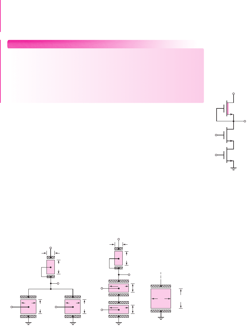
The NMOS NAND logic gate contains additional driver transistors connected in
series. Figure 16.13 shows a two-input NMOS NAND logic gate with a depletion
load. If both
A = B = logic 0
, or if either A or B is a logic 0, at least one driver is cut
off, and the output is high. If both
A = B = logic 1
, then the composite driver of the
NMOS inverter conducts and the output goes low.
Since the gate-to-source voltages of
M
DA
and
M
DB
are not equal, determining
the actual voltage
V
OL
of a NAND gate is difficult. The drain-to-source voltages of
M
DA
and
M
DB
must adjust themselves to produce the same current. In addition, if
the body effect is also included, the analysis becomes even more difficult. Since the
two driver transistors are in series, a good approximation assumes that the width-to-
length ratio of the drivers must be twice that of a single driver in an NMOS inverter
to achieve a given
V
OL
value.
The composite width-to-length ratios of the driver transistors in the two-input
NMOS NOR and NAND gates are shown schematically in Figure 16.14. For the
NOR gate, the effective width doubles; for the NAND gates, the effective length
doubles.
A
v
O
V
DD
M
DA
B
M
DB
M
L
Figure 16.13 Two-input
NMOS NAND logic gate
with depletion load
W
B
L
B
B
W
A
L
A
A
Y
W
L
L
L
V
DD
(a) (b)
W
A
≡
L
A
+ L
B
W
L
L
L
V
DD
Y
W
B
L
B
B
W
A
L
A
A
Figure 16.14 Composite width-to-length ratios of driver transistors in two-input NMOS
logic configurations (a) NOR and (b) NAND
nea80644_ch16_1145-1254.qxd 07/12/2009 3:37 Page 1165 pinnacle MHDQ-New:MHDQ134:MHDQ134-16:

1166 Part 3 Digital Electronics
EXAMPLE 16.6
Objective: Determine the low output voltage of an NMOS NAND circuit.
Consider the NAND logic circuit shown in Figure 16.13 biased at
V
DD
= 2.5
V.
Assume transistor parameters of
k
n
= 100 μ
A/V
2
,
V
TND
= 0.4
V,
V
TNL
=−0.6
V,
(W/L)
D
= 8
, and
(W/L)
L
= 1
. Neglect the body effect.
Solution: If either
A
or
B
is a logic 0, then
v
O
=
logic 1
= 2.5
V.
If
A = B =
logic 1
= 2.5
V, then both driver transistors are driven in the non-
saturation region and the output goes low. As a good approximation, we will assume
the effective length of the driver transistor doubles. Then, using Equation (16.27(b)),
we have
1
2
·
W
L
D
W
L
L
2(v
I
− V
TND
)v
O
−v
2
O
=
(
−V
TNL
)
2
or
8
(2)(1)
2(2.5 − 0.4)v
O
−v
2
O
= [−(−0.6)]
2
The output voltage is found to be
v
O
= 21.5
mV.
This output voltage is the same value that would be obtained for a simple
inverter with
(W/L)
D
= 4
and
(W/L)
L
= 1
.
Comment: If an N-input NMOS NAND logic gate were to be fabricated then the
width-to-length ratio of the drivers would need to be N times that of a single driver in
an NMOS inverter to achieve a given value of
V
OL
. The increase in the required area
of the driver transistors in a NAND logic gate means that logic gates with more than
three or four inputs are not attractive.
EXERCISE PROBLEM
Ex 16.6: Repeat Example 16.6 for a three-input NMOS NAND logic gate with
depletion load with
(W/L)
L
= 1
and (a)
(W/L)
D
= 12
and (b)
(W/L)
D
= 4
.
(Ans. (a)
v
O
= 21.5
mV, (b)
v
O
= 65.3
mV)
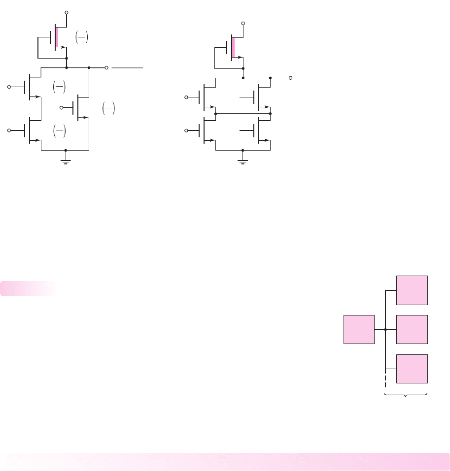
NMOS Logic Circuits
The series–parallel combination of drivers can be expanded to synthesize more com-
plex logic functions. Consider the circuit in Figure 16.15. We can show that the
Boolean output function is
f =
(A · B + C)
Also, the individual transistor width-to-length ratios shown produce an effective
K
D
/K
L
ratio of 4 for an effective single inverter when only
M
DA
and
M
DB
are con-
ducting, or only
M
DC
is conducting. The actual complexity of the Boolean function
is limited since the required width-to-length ratios of individual transistors may be-
come unreasonably large.
Two additional logic functions are the exclusive-OR and exclusive-NOR.
Figure 16.16 shows a circuit configuration that produces the exclusive-OR function.
16.2.2
nea80644_ch16_1145-1254.qxd 07/12/2009 3:37 Page 1166 pinnacle MHDQ-New:MHDQ134:MHDQ134-16:
Chapter 16 MOSFET Digital Circuits 1167
If
A = B = logic 1
, a path exists from the output to ground through drivers
M
DA
and
M
DB
, and the output goes low. Similarly, if
A = B = logic 0
, which means that
¯
A =
¯
B = logic 1
, a path exists from the output to ground through the drivers
M
D
¯
B
and
M
D
¯
A
, and the output again goes low. For all other input logic signal combina-
tions, the output is isolated from ground so the output goes high.
Fanout
An NMOS inverter or NMOS logic gate must be capable of driving more than one
load, as shown in Figure 16.17. It is assumed that each load is identical to the driver
logic circuit. The number of identical-load circuits connected to the output of a dri-
ver logic circuit is defined as the fanout. For MOS logic circuits, the inputs to the
load circuits are the oxide-insulated gates of the MOS transistors; therefore, the static
loading caused by multiple driver loads is so small that the dc transfer curve is
essentially identical to a no-load condition. The dc characteristics of MOS logic
circuits are unaffected by the fanout to other MOS logic inputs. However, the load
capacitance due to a large fanout seriously degrades the switching speed and propa-
gation delay times. Consequently, maintaining the propagation delay time below a
specified maximum value determines the fanout of MOS digital circuits.
16.2.3
A
v
O
= f =
(A
⋅
B + C)
V
DD
C
B
1
1
M
DC
4
1
M
DA
8
1
M
DB
8
1
M
L
Figure 16.15 NMOS logic circuit example
A
V
DD
A
M
DA
M
DA
B
B M
DB
M
DB
−
−
−
−
f = A ⊗ B
M
L
Figure 16.16 NMOS exclusive-OR logic gate
Load
circuit
Load
circuit
Driving
logic
circuit
N load circuits
Load
circuit
Figure 16.17 Logic circuit
driving N load circuits
Test Your Understanding
TYU 16.4 (a) Design a three-input NMOS NOR logic gate with depletion load such
that
V
OL
(max) = 50
mV and such that the maximum power dissipation is
50 μ
W.
Let
V
DD
= 2.5
V. The transistor parameters are
k
n
= 100 μ
A/V
2
,
V
TND
= 0.4
V,
and
V
TNL
=−0.6
V. (b) Using the results of part (a), determine
V
OL
when all inputs
are a logic 1. (Ans. (a)
(W/L)
L
= 1.11
,
(W/L)
D
= 1.93
; (b)
V
OL
= 16.5
mV)
TYU 16.5 Consider the NMOS logic circuit in Figure 16.18. Assume transistor
parameters of
k
n
= 100 μA/V
2
and
V
TN
= 0.4
V. Assume all driver transistors are
identical. Neglect the body effect. (a) If
(W/L)
L
= 0.5
, determine
(W/L)
for the
drivers such that
V
OL
(max) = 80 μ
V. Assume logic 1 input voltages are 2.1 V.
nea80644_ch16_1145-1254.qxd 07/12/2009 3:37 Page 1167 pinnacle MHDQ-New:MHDQ134:MHDQ134-16: