Neamen D. Microelectronics: Circuit Analysis and Design
Подождите немного. Документ загружается.

1188 Part 3 Digital Electronics
design by considering the NMOS portion of the circuit. To implement a basic OR
(NOR) function, the n-channel transistors are in parallel (Figure 16.33) and to im-
plement a basic AND (NAND) function, the n-channel transistors are in series (Fig-
ure 16.34). We will consider whether the function or its complement is generated at
the end of the design.
Solution (NMOS Design): In the overall function, we note the logic OR between the
functions AB and
C(D + E)
, so that the NMOS devices used to implement AB will
be in parallel with the NMOS devices used to implement
C(D + E)
. There is a logic
AND between the inputs A and B, so that the NMOS devices with these inputs will
be in series. Finally, the NMOS devices with the D and E inputs will be in parallel
and this combination will be in series with the NMOS device with the C input. The
NMOS implementation of the function is shown in Figure 16.39.
Solution (PMOS Design): The arrangement of the PMOS devices is complementary
to that of the NMOS devices. PMOS devices that perform the basic OR function are
in series and PMOS devices that perform the basic AND function are in parallel. We
then see that the PMOS devices used to implement AB will be in series with the de-
vices used to implement
C(D + E)
. The two PMOS devices with the A and B inputs
will be in parallel. The two PMOS devices with the D and E inputs will be in series
and in turn will be in parallel with the PMOS device with the C input. The completed
circuit is shown in Figure 16.40.
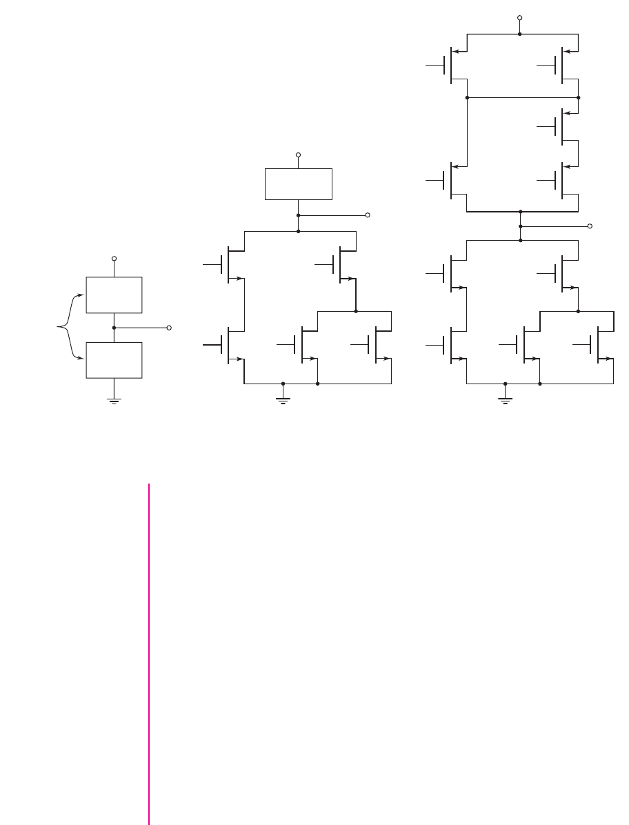
PMOS
NMOS
A, B, C, D, E
V
DD
Y
Figure 16.38 General CMOS
design
PMOS
network
V
DD
V
O
M
NC
M
NA
M
ND
M
NE
EDB
AC
M
NB
Figure 16.39 NMOS design for
Example 16.11
V
DD
M
PA
M
PB
A
M
PC
C
B
M
PD
D
M
PE
E
M
NA
A
M
NB
B
M
ND
D
M
N
E
E
M
NC
V
O
C
Figure 16.40 Complete CMOS design
for Example 16.11
nea80644_ch16_1145-1254.qxd 07/12/2009 3:37 Page 1188 pinnacle MHDQ-New:MHDQ134:MHDQ134-16:

Chapter 16 MOSFET Digital Circuits 1189
Final Solution: By considering various inputs, we may note that the output signal of
the circuit shown in Figure 16.40 is actually the complement of the desired signal.
We may then simply add a CMOS inverter to the output to obtain the desired
function.
Comment: As mentioned, there are formal ways in which to design circuits. How-
ever, in many cases, these circuits can be designed by using the knowledge and intu-
ition gained from previous work. The width-to-length ratios of the various transistors
can be determined as we have done in previous examples.
EXERCISE PROBLEM
Ex 16.11: Design the width-to-length ratios of the transistors in the static CMOS
logic circuit of Figure 16.40. Symmetrical switching times are desired and the
switching times should correspond to the basic CMOS inverter. (Ans. All NMOS
devices,
W
n
= 2W
;
W
p
(M
PA
) = W
p
(M
PB
) = W
p
(M
PC
) = 4W
;
W
p
(M
PD
) =
W
p
(M
PE
) = 8W
)
Another example of a CMOS logic gate is the exclusive-OR or XOR. The logic
function can be written as
F
XOR
=
¯
AB + A
¯
B
(16.70)
We have noticed that the output of the CMOS gates is actually the complement of the
input signal. We can therefore write
¯
F
XOR
= F
XNOR
=
¯
A
¯
B + AB
(16.71)
Assuming that input signals A, B,
¯
A
, and
¯
B
are available, Figure 16.41 shows a
CMOS static implementation of the logic function.
We may note that
¯
A
¯
B
as well as AB means two NMOS devices in series and two
PMOS devices in parallel. The OR function means the combination of NMOS
BA
B
A
B
A
F
A
B
V
DD
M
PA
M
PB
M
PB
M
PA
M
NA
M
NA
M
NB
M
NB
–
––
–
–
–
–
–
Figure 16.41 A CMOS static exclusive-OR logic gate
nea80644_ch16_1145-1254.qxd 07/12/2009 3:37 Page 1189 pinnacle MHDQ-New:MHDQ134:MHDQ134-16:
1190 Part 3 Digital Electronics
devices is in parallel and the combination of PMOS devices is in series. This design
is shown in the figure. In considering the truth table for the exclusive-OR function,
we may note that the output of the circuit in Figure 16.41 is indeed the exclusive-OR
function. In the design of CMOS logic gates, then, we should actually design the
complement of the desired function.
In the PMOS portion of the design, there should be an electrical connection be-
tween the drains of
M
PA
and
M
PB
. This connection is shown as a dotted line, but is
not actually required. The only pull-up conditions are for
A =
¯
B = 0
and for
¯
A = B = 0
, which are achieved without this connection.
Fanout and Propagation Delay Time
Fanout
The term fanout refers to the number of load gates of similar design connected to the
output of a driver gate. The maximum fanout is the maximum number of load gates
that may be connected to the output. Since the CMOS logic gate will be driving other
CMOS logic gates, the quiescent current required to drive the other CMOS gates is
essentially zero. In terms of static characteristics, the maximum fanout is virtually
limitless.
However, each additional load gate increases the load capacitance that must be
charged and discharged as the driver gate changes state, and this places a practical
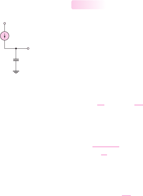
limit on the maximum allowable number of load gates. Figure 16.42 shows a con-
stant current charging a load capacitance. The voltage across the capacitance is
v
O
=
1
C
L
I
O
dt =
I
O
t
C
L
(16.72)
The load capacitance
C
L
is proportional to the number N of load gates and to the
input gate capacitance of each load. The current
I
O
is proportional to the conduction
parameter of the driver transistor. The switching time is therefore
t ∝
N(W · L)
L
W
L
D
(16.73)
where the gate capacitance is directly proportional to the gate area of the load
(W · L)
L
, and the conduction parameter of the driver transistor is proportional to the
width-to-length ratio. Equation (16.73) can be rewritten as
t ∝ N(L
L
L
D
)
W
L
W
D
(16.74)
The propagation delay time, which is proportional to the switching time, in-
creases as the fanout increases. The propagation delay time could be reduced by in-
creasing the size of the driver transistor. However, in any given driver logic circuit
and load logic circuit, the sizes of the devices are generally fixed. Consequently, the
maximum fanout is limited by the maximum acceptable propagation delay time.
Propagation delay times are typically measured with a specified load capaci-
tance. The average propagation delay time of a two-input CMOS NOR gate (such as
an SN74HC36) is 25 ns, measured with a load capacitance of
C
L
= 50 pF
. Since the
input capacitance is
C
I
= 10 pF
, a fanout of five would produce a 50 pF load capac-
itance. A fanout larger than five would increase the load capacitance, and would also
increase the propagation delay time above the specified value.
16.4.4
V
DD
I
O
v
O
C
L
Figure 16.42 Constant-
current source charging
a load capacitor
nea80644_ch16_1145-1254.qxd 07/12/2009 3:37 Page 1190 pinnacle MHDQ-New:MHDQ134:MHDQ134-16:

Chapter 16 MOSFET Digital Circuits 1191
Propagation Delay Time
Although the propagation delay time of the CMOS inverter can be determined by
analytical techniques, it can also be determined by computer simulation. This is espe-
cially true when more complex CMOS logic circuits are considered. Using the appro-
priate transistor models in the simulation, the transient response can be produced.
Obtaining an accurate transient response depends on using the correct transistor para-
meters. Some computer simulation problems in the end-of-chapter problems deal
with propagation delay times. However, we will not go into detail here.
Test Your Understanding
TYU 16.9 Design a static CMOS logic circuit that implements the logic function
Y = (
ABC + DE)
. (Ans. NMOS design: A, B, C inputs to three NMOS devices in
series and D, E inputs to two NMOS devices in series; then, three NMOS and two
NMOS in parallel)
TYU 16.10 Design the width-to-length ratios of the transistors in the static CMOS
exclusive-OR logic gate in Figure 16.41. Symmetrical switching times are desired
and the switching times should correspond to the basic CMOS inverter. (Ans. All
NMOS,
W
n
= 2W
; all PMOS,
W
p
= 4W
)
16.5 CLOCKED CMOS LOGIC CIRCUITS
Objective: • Analyze and design clocked CMOS logic gates.
The CMOS logic circuits considered in the previous section are called static circuits.
One characteristic of a static CMOS logic circuit is that the output node always has a
low-resistance path to either ground or
V
DD
. This implies that the output voltage is
well defined and is never left floating.
Static CMOS logic circuits can be redesigned with an added clock signal while
at the same time eliminating many of the PMOS devices. In general, the PMOS de-
vices must be larger than NMOS devices. Eliminating as many PMOS devices as
possible reduces the required chip area as well as the input capacitance. The low-
power dissipation of the CMOS technology, however, is maintained.
Clocked CMOS circuits are dynamic circuits that generally precharge the out-
put node to a particular level when the clock is at a logic 0. Consider the circuit in
Figure 16.43. When the clock signal is low, or
CLK = logic 0
,
M
N1
is cut off and
the current in the circuit is zero. Transistor
M
P1
is in a conducting state, but since
the current is zero, then
v
O1
charges to
V
DD
. A high input to the CMOS inverter
means that
v
O
= 0
. During this phase of the clock signal, the gate of
M
P2
is
precharged.
During the next phase, when the clock signal goes high, or CLK =logic 1, tran-
sistor
M
P1
cuts off and
M
N1
is biased in a conducting state. If input
A = logic 0
, then
M
NA
is cut off and there is no discharge path for voltage
v
O1
; therefore,
v
O1
remains
charged at
v
O1
= V
DD
. However, if CLK = logic 1 and
A = logic 1
, then both
M
N1
and
M
NA
are biased in a conducting state, providing a discharge path for voltage
v
O1
.
As
v
O1
is pulled low, output signal
v
O
goes high.
nea80644_ch16_1145-1254.qxd 07/12/2009 3:37 Page 1191 pinnacle MHDQ-New:MHDQ134:MHDQ134-16:
1192 Part 3 Digital Electronics
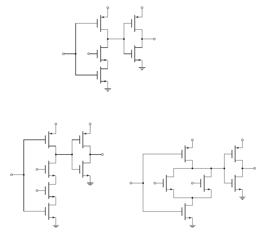
A
v
O
V
DD
V
DD
M
NA
B
M
NB
M
N1
M
P1
v
o1
M
N2
CLK
M
P2
A
v
O
V
DD
V
DD
M
N1
M
P1
v
o1
M
N2
CLK
M
P2
M
NA
B
M
NB
(a) (b)
Figure 16.44 Clocked CMOS logic circuit: (a) AND function and (b) OR function
The quiescent power dissipation in this circuit is essentially zero, as it was in the
standard CMOS circuits. A small amount of power is required to precharge output
v
O1
, if it had been pulled low during the previous half clock cycle.
The single NMOS transistor
M
NA
in Figure 16.43 can be replaced by a more
complex NMOS logic circuit. Consider the two circuits in Figure 16.44. When
CLK =logic 0, then
M
N1
cuts off and
M
P1
is in its conducting state in both circuits;
then,
v
O1
is charged to
v
O1
= V
DD
and
v
O
= 0
. For the circuit in Figure 16.44(a),
when CLK = logic 1, voltage
v
O1
is discharged to ground or pulled low only when
A = B = logic 1
. In this case,
v
O
goes high. The circuit in Figure 16.44(a) performs
the AND function. Similarly, the circuit in Figure 16.44(b) performs the OR
function.
The advantage of the precharge technique is that it avoids the use of extensive pull-
up networks: Only one PMOS and one NMOS transistor are required. This leads to an
almost 50 percent savings in silicon area for larger circuits, and a reduction in capaci-
tance resulting in higher speed. In addition, the static or quiescent power dissipation is
essentially zero, so the circuit maintains the characteristics of CMOS circuits.
A
v
O1
v
O
V
DD
V
DD
M
NA
M
N1
M
P1
M
P2
M
N2
CLK
Figure 16.43 Simple clocked CMOS logic circuit
nea80644_ch16_1145-1254.qxd 07/12/2009 3:37 Page 1192 pinnacle MHDQ-New:MHDQ134:MHDQ134-16:
Chapter 16 MOSFET Digital Circuits 1193
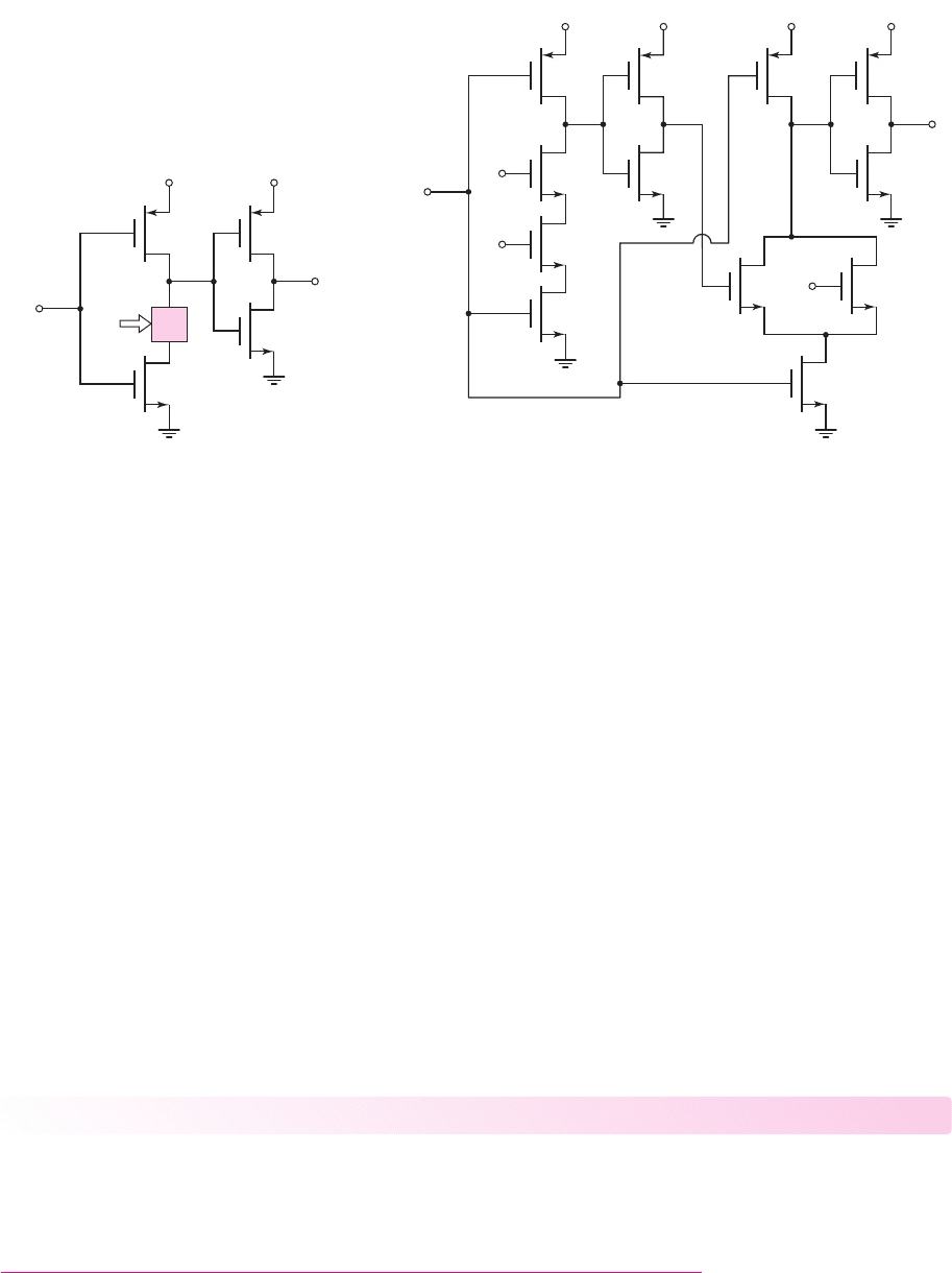
f(X)
V
DD
V
DD
M
N1
M
P1
M
N2
CLK
M
P2
f
X
Figure 16.45 Generalized CMOS clocked
logic circuit
The AND and OR logic transistors
M
NA
and
M
NB
in Figures 16.44(a) and
16.44(b) can be replaced by a generalized logic network as indicated in Figure 16.45.
The box marked f is an NMOS pull-down network that performs a particular logic
function
f (X)
of n variables, where
X = (x
1
, x
2
,...,x
n
)
. The NMOS circuit is a
combination of series–parallel interconnections of n transistors. When the clock sig-
nal goes high, the CMOS inverter output is the logic function
f (X)
.
The set of X inputs to the logic circuits f is derived from the outputs of other
CMOS inverters and clocked logic circuits. The means that when CLK = logic 0, the
outputs of all CMOS inverters are a logic 0 during the precharge cycle. As a result, all
n variables
X = (x
1
, x
2
,...,x
n
)
are a logic 0 during the precharge cycle. During this
time, all NMOS transistors are cut off, which guarantees that output
v
O1
can be
precharged to
V
DD
. There can then be only one possible transition at each node during
the evaluation phase. The output of the CMOS buffer may change from a 0 to a 1.
An example of a cascaded domino CMOS circuit is shown in Figure 16.46. Dur-
ing the precharge cycle, in which CLK =logic 0, nodes 1 and 3 are charged high and
nodes 2 and 4 are low. Also during this time, the inputs A, B, and C are all a logic 0.
During the evaluation phase, in which CLK = logic 1, if
A = C = logic 1
and
B = logic 0
, then node 1 remains charged high,
f
1
= logic 0
, and node 3 discharges
through
M
NC
causing
f
2
to go high. However, if, during the evaluation phase,
A = B = logic 1
and
C = logic 0
, then node 1 is pulled low causing
f
1
to go high,
which in turn causes node 3 to go low and forces node 4 high. This chain of actions
thus leads to the term domino circuit.
Test Your Understanding
TYU 16.11 Design a clocked CMOS domino logic circuit, such as shown in Fig-
ure 16.45, to generate an output
f (X) = A · B · C + D · E
.
TYU 16.12 Sketch a clocked CMOS logic circuit that realizes the exclusive OR
function.
A
V
DD
V
DD
V
DD
V
DD
M
NA
B
M
NB
M
N1
f
1
M
P1
M
N2
CLK
M
P2
M
N4
M
P4
f
2
(2) (3) (4)(1)
M
P3
M
N3
M
Nf
C
M
NC
Figure 16.46 Cascaded clocked or domino CMOS logic circuit
nea80644_ch16_1145-1254.qxd 07/12/2009 3:38 Page 1193 pinnacle MHDQ-New:MHDQ134:MHDQ134-16:
1194 Part 3 Digital Electronics
16.6 TRANSMISSION GATES
Objective: • Analyze and understand the characteristics of NMOS
and CMOS transmission gates.
Transistors can act as switches between driving circuits and load circuits. Transistors
used to perform this function are called transmission gates. We will examine NMOS and
CMOS transmission gates, which can also be configured to perform logic functions.
NMOS Transmission Gate
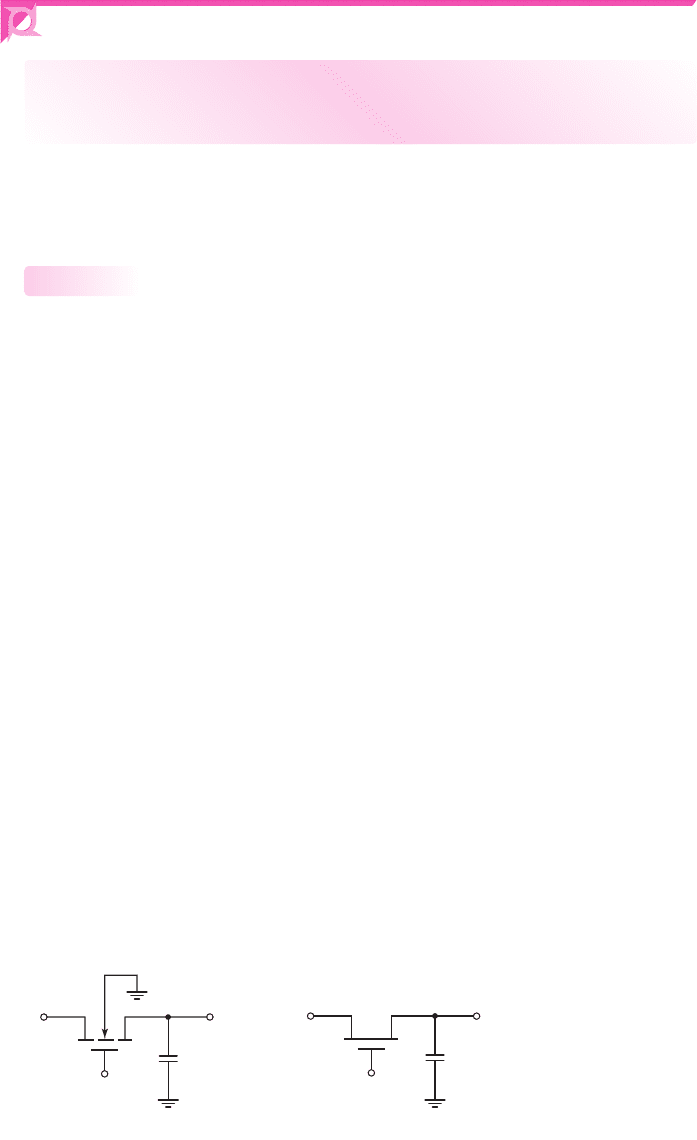
The NMOS enhancement-mode transistor in Figure 16.47(a) is a transmission gate
connected to a load capacitance
C
L
, which could be the input gate capacitance of a
MOS logic circuit. In this circuit, the transistor must be bilateral, which means it
must be able to conduct current in either direction. This is a natural feature of MOS-
FETs. Terminals a and b are assumed to be equivalent, and the bias applied to the
transistor determines which terminal acts as the drain and which terminal acts as the
source. The substrate must be connected to the most negative potential in the circuit,
which is usually ground. Figure 16.47(b) shows a simplified circuit symbol for the
NMOS transmission gate that is used extensively.
We assume that the NMOS transmission gate is to operate over a voltage range
of zero-to-
V
DD
. If the gate voltage
φ
is zero, then the n-channel transistor is cut off
and the output is isolated from the input. The transistor is essentially an open switch.
If
φ = V
DD
,
v
I
= V
DD
, and
v
O
is initially zero, then terminal a acts as the drain
since its bias is
V
DD
, and terminal b acts as the source since its bias is zero. Current en-
ters the drain from the input, charging up the capacitor. The gate-to-source voltage is
v
GS
= φ − v
O
= V
DD
−v
O
(16.75)
As the capacitor charges and
v
O
increases, the gate-to-source voltage decreases. The
capacitor stops charging when the current goes to zero. This occurs when the gate-
to-source voltage
v
GS
becomes equal to the threshold voltage
V
TN
. The maximum
output voltage occurs when
v
GS
= V
TN
, therefore, from Equation (16.75), we have
v
GS
(min) = V
TN
= V
DD
−v
O
(max)
(16.76(a))
or
v
O
(max) = V
DD
− V
TN
(16.76(b))
16.6.1
C
L
ba
ff
v
I
v
O
C
L
ba
v
I
v
O
(a) (b)
Figure 16.47 (a) NMOS transmission gate, showing substrate connection, and (b) simplified
diagram
nea80644_ch16_1145-1254.qxd 07/12/2009 3:38 Page 1194 pinnacle MHDQ-New:MHDQ134:MHDQ134-16:
Chapter 16 MOSFET Digital Circuits 1195
where
V
TN
is the threshold voltage taking into account the body effect.
Equation (16.76(b)) demonstrates one disadvantage of an NMOS transmission
gate. A logic 1 level degrades, or attenuates, as it passes through the transmission gate.
However, this may not be a serious problem for many applications.
Figure 16.48 shows the quasi-static output voltage versus input voltage of the
NMOS transmission gate. As seen in the figure, when
v
I
= V
DD
, the output voltage
is
v
O
= V
DD
− V
TN
as we have discussed. For input voltages in the range
v
I
<
V
DD
− V
TN
, the figure demonstrates that
v
O
= v
I
. In this range of input voltages,
the gate-to-source voltage is still greater than the threshold voltage. However, in
steady-state, the current must be zero through the capacitor. In this case, the current
becomes zero when the drain-to-source voltage is zero, or when
v
O
= v
I
.
Now consider the situation in which
φ = V
DD
,
v
I
= 0
, and
v
O
= V
DD
− V
TN
initially. Terminal b then acts as the drain and terminal a acts as the source. The gate-
to-source voltage is
v
GS
= φ − v
I
= V
DD
−0 = V
DD
(16.77)
The value of
v
GS
is a constant, and the capacitor discharges as current enters the NMOS
transistor drain. The capacitor stops discharging when the current goes to zero. Since
v
GS
is a constant at
V
DD
, the drain current goes to zero when the drain-to-source volt-
age is zero, which means that the capacitor completely discharges to zero. This implies
that a logic 0 is transmitted unattenuated through the NMOS transmission gate.
Using an NMOS transmission gate in a MOS circuit may introduce a dynamic
condition. Figure 16.49 shows a cross section of the NMOS transistor in the trans-
mission gate configuration. If
v
I
= φ = V
DD
, then the load capacitor charges to
v
O
v
I
V
DD
– V
TN
V
DD
– V
TN
V
DD
0
Figure 16.48 Output voltage versus input voltage
characteristics of the NMOS transmission gate
p
a
f
b
v
O
C
L
i
L
v
I
n
n
Figure 16.49 NMOS transmission gate with cross
section of NMOS transistor
nea80644_ch16_1145-1254.qxd 07/12/2009 3:38 Page 1195 pinnacle MHDQ-New:MHDQ134:MHDQ134-16:

1196 Part 3 Digital Electronics
EXAMPLE 16.12
Objective: Estimate the rate at which the output voltage
v
O
in Figure 16.49 de-
creases with time when the NMOS transmission gate transistor is in its off state.
Assume the capacitor is initially charged to
v
O
= 2.9
V. Let
C
L
= 0.2
pF and as-
sume the reverse-biased pn junction leakage current is a constant at
i
L
= 100
pA.
Solution: The voltage across the capacitor can be written as
v
O
=−
1
C
L
i
L
dt =−
i
L
C
L
t + K
1
where
K
1
= v
O
(t = 0) = 2.9
V is the initial condition. Therefore,
v
O
(t) = 2.9 −
i
L
C
L
t
The rate at which the output voltage decreases is
dv
O
dt
=−
i
L
C
L
=−
100 × 10
−12
0.2 × 10
−12
=−500 V/s ⇒−0.5V/ms
Therefore, in this example, the capacitor would completely discharge in 5.8 ms.
Comment: Even though the NMOS transmission gate may introduce a dynamic con-
dition into a circuit, this gate is still useful in clocked logic circuits in which a clock
signal is periodically applied to the NMOS transistor gate. If, for example, the clock
frequency is 25 kHz, the clock pulse period is
40 μ
s, which means that the output
voltage would decay by only approximately 0.7 percent during a clock period.
EXERCISE PROBLEM
Ex 16.12: The threshold voltage of the NMOS transmission gate transistor in Figure
16.47(a) is
V
TN
= 0.4
V. Determine the output voltage
v
O
for: (a)
v
I
= φ = 2.5
V;
(b)
v
I
= 1.8
V,
φ = 2.5
V; (c)
v
I
= 2.3
V,
φ = 2.5
V; and (d)
v
I
= 2.5
V,
φ = 1.5
V. Neglect the body effect. (Ans. (a)
v
O
= 2.1
V, (b)
v
O
= 1.8
V,
(c)
v
O
= 2.1
V, (d)
v
O
= 1.1
V)
EXAMPLE 16.13
Objective: Determine the output of an NMOS inverter driven by a series of NMOS
transmission gates.
Consider the circuit shown in Figure 16.50. The NMOS inverter is driven by
three NMOS transmission gates in series. Assume the threshold voltages of the
NMOS transmission gate transistors and the NMOS driver transistor are
v
O
= V
DD
− V
TN
. When
φ = 0
, the NMOS device turns off and the input and out-
put become isolated.
The capacitor voltage reverse biases the pn junction between terminal b and
ground. A reverse-biased pn junction leakage current begins to discharge the capaci-
tor, and the circuit does not remain in a static condition. This circuit is now dynamic
in that the high output does not remain constant with time.
nea80644_ch16_1145-1254.qxd 07/15/2009 09:31 PM Page 1196 F506 Hard disk:Desktop Folder:ALI-07-15-09:
Chapter 16 MOSFET Digital Circuits 1197
V
TN
= 0.4
V, and the threshold voltage of the load transistor is
V
TNL
=−0.6
V. Let
K
D
/K
L
= 3
for the inverter. Determine
v
O
for
v
I
= 0
and
v
I
= 2.5
V
Solution: The three NMOS transmission gates in series act as an AND/NAND func-
tion. If
v
I
= 0
and
A = B = C =
logic 1
= 2.5
V, the gate capacitance to driver
M
D
becomes completely discharged, which means that
v
O1
= v
O2
= v
O3
= 0
. Driver
M
D
is cut off and
v
O
= 2.5
V.
If
v
I
= 2.5
V and
A = B = C =
logic 1
= 2.5
V, the three transmission gates
are biased in their conducting state, and the gate capacitance of
M
D
becomes
charged. For transistor
M
NA
, the current becomes zero when the gate-to-source volt-
age is equal to the threshold voltage, or, from Equation (16.76(b)),
v
O1
= V
DD
− V
TN
= 2.5 −0.4 = 2.1V
Transistors
M
NB
and
M
NC
also cut off when the gate-to-source voltages are equal to
the threshold voltage; therefore
v
O2
= v
O3
= V
DD
− V
TN
= 2.5 −0.4 = 2.1V
This result shows that the drain-to-source voltages of
M
NB
and
M
NC
are also
zero. A threshold voltage drop is lost in the first transmission gate, but additional
threshold voltage drops are not lost in subsequent NMOS transmission gates in
series.
For a voltage of
v
O3
= 2.1
V applied to the gate of
M
D
, the driver is biased in
the nonsaturation region and the load is biased in the saturation region. From
i
DD
= i
DL
, we have
K
D
2(v
O3
− V
TN
)v
O
−v
2
O
= K
L
[−V
TNL
]
2
The output voltage is found to be
v
O
= 35.7
mV.
If any one of the transmission gate voltages, A or B or C, switches to a logic 0, then
v
O3
will begin to discharge through a reverse-biased pn junction in the transmission
gates, which means that
v
O
will increase with time.
Comment: In this example, the inverter is again in a dynamic condition; that is,
when any transmission gate is cut off, the output voltage changes with time. How-
ever, this type of circuit can be used in clocked digital systems.
v
O
v
I
V
DD
= 2.5 V
M
D
CBA
v
O3
v
O2
v
O1
M
NA
M
NB
M
NC
i
DL
i
DD
M
L
Figure 16.50 NMOS inverter driven by three NMOS transmission gates
in series
nea80644_ch16_1145-1254.qxd 07/12/2009 3:38 Page 1197 pinnacle MHDQ-New:MHDQ134:MHDQ134-16: