Neamen D. Microelectronics: Circuit Analysis and Design
Подождите немного. Документ загружается.

1168 Part 3 Digital Electronics
(b) Determine the maximum power dissipation in the logic circuit. (Ans. (a)
(W/L)
D
=
15.4
,(b)
P = 255 μ
W)
TYU 16.6 Repeat Exercise TYU 16.5 for the NMOS logic circuit in Figure
16.19, except assume the threshold voltage of the load device is
V
TNL
=−0.6
V.
(Ans. (a)
(W/L)
D
= 1.09
,(b)
P = 22.5 μ
W)
16.3 CMOS INVERTER
Objective: • Analyze and design CMOS inverters.
Complementary MOS, or CMOS, circuits contain both n-channel and p-channel
MOSFETs. As we will see, the power dissipation in CMOS logic circuits is much
smaller than in NMOS circuits, which makes CMOS very attractive. We briefly re-
view the characteristics of p-channel transistors, and will then analyze the CMOS in-
verter, which is the basis of most CMOS logic circuits. We will examine the CMOS
NOR and NAND gates and other basic CMOS logic circuits, covering power dissi-
pation, noise margin, fanout, and switching characteristics.
p-Channel MOSFET Revisited
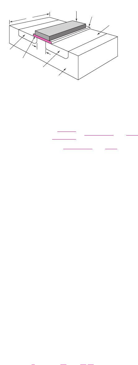
Figure 16.20 shows a simplified view of a p-channel MOSFET. The p- and n-regions
are reversed from those in an n-channel device. Again, the channel length is L and the
channel width is W. Usually in any given fabrication process, the channel length is
the same for all devices, so the channel width W is the variable in logic circuit design.
Normally, in an integrated circuit, more than one p-channel device will be fabri-
cated in the same n-substrate so the p-channel transistors will exhibit a body effect.
The n-substrate is connected to the most positive potential. The source terminal may
16.3.1
A
C
v
O
V
DD
= 5 V
B
M
DA
M
L
M
DB
M
DC
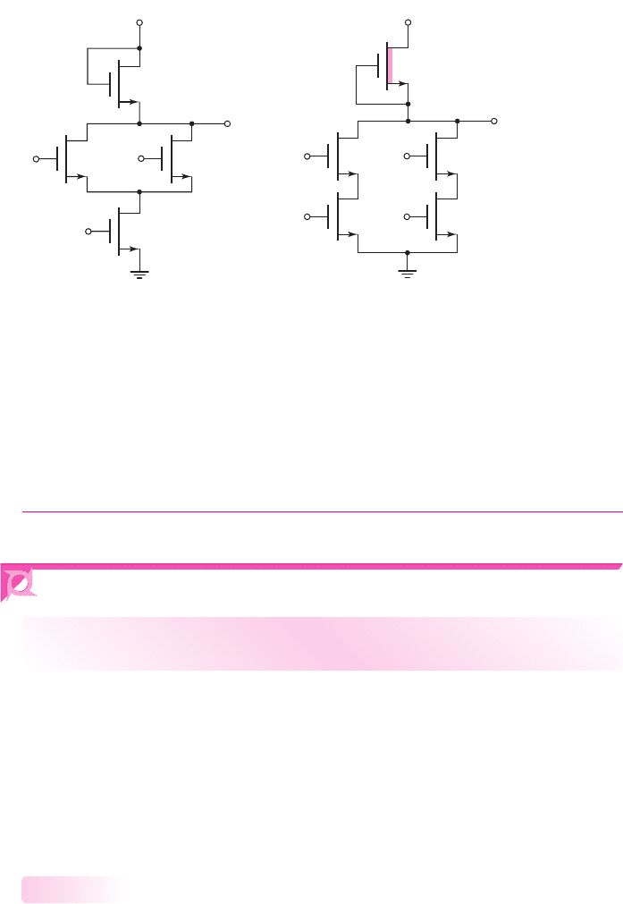
Figure 16.18 Figure for Exercise
TYU 16.5
A
V
DD
= 5 V
v
O
B
M
DB
M
DA
C
D
M
DD
M
DC
M
L
Figure 16.19 Figure for Exercise
TYU 16.6
nea80644_ch16_1145-1254.qxd 07/12/2009 3:37 Page 1168 pinnacle MHDQ-New:MHDQ134:MHDQ134-16:
Chapter 16 MOSFET Digital Circuits 1169
be negative with respect to the substrate; therefore, voltage
V
BS
may exist between
the body and the source. The threshold voltage is
V
TP
= V
TPO
−
√
2eε
s
N
d
C
ox
2φ
fn
+ V
BS
−
2φ
fn
= V
TPO
−γ
2φ
fn
+ V
BS
−
2φ
fn
(16.30)
where
V
TPO
is the threshold voltage for zero body-to-source voltage, or
V
BS
= 0
.
The parameter
N
d
is the n-substrate doping concentration and
φ
fn
is a potential re-
lated to the substrate doping. The parameter
γ
is the body effect coefficient.
Current–Voltage Relation
The current–voltage characteristics of the p-channel MOSFET are functions of both
the electrical and geometric properties of the device. When the transistor is biased in
the nonsaturation region, we have
v
SD
≤ v
SG
+ V
TP
. Therefore,
i
D
= K
p
2(v
SG
+ V
TP
)v
SD
−v
2
SD
(16.31(a))
In the saturation region, we have
v
SD
≥ v
SG
+ V
TP
, which means that
i
D
= K
p
(v
SG
+ V
TP
)
2
(16.31(b))
The gate potential is negative with respect to the source. For the p-channel
transistor to conduct, we must have
v
GS
< V
TP
, where
V
TP
is negative for an
enhancement-mode device. We also see that
v
SG
> |V
TP
|
when the p-channel device
is conducting.
In most cases, the channel length modulation factor
λ
has very little effect on the
operating characteristics of MOS digital circuits. Therefore, the term
λ
is assumed to
be zero unless otherwise stated.
The transition point, which separates the nonsaturation and saturation bias
regions, is given by
v
SD
= v
SD
(sat) = v
SG
+ V
TP
(16.32)
The parameter
K
p
is the conduction parameter and is given by
K
p
=
1
2
μ
p
C
ox
W
L
=
k
p
2
W
L
(16.33)
L
W
Polysilicon
or metal
Oxide
Gate
p-type
semiconducto
r
p-source
p-drain
n-substrate
Figure 16.20 Simplified cross section of p-channel
MOSFET
nea80644_ch16_1145-1254.qxd 07/12/2009 3:37 Page 1169 pinnacle MHDQ-New:MHDQ134:MHDQ134-16:
1170 Part 3 Digital Electronics
As before, the hole mobility
μ
p
and oxide capacitance
C
ox
are assumed to be
constant for all devices. The hole mobility in p-channel silicon MOSFETs is approx-
imately one-half the electron mobility
μ
n
in n-channel silicon MOSFETs. This
means that a p-channel device width must be approximately twice as large as that of
an n-channel device in order that the two devices be electrically equivalent (that is,
that they have the same conduction parameter values).
Small Geometry Effects
The same small geometry effects apply to the p-channel devices as we discussed for
the n-channel devices in Section 16.1.1. As with the NMOS inverters and logic cir-
cuits, we can use Equations (16.31(a)), (16.31(b)), and (16.32) as first-order equa-
tions in the design of CMOS logic circuits. The basic operation and behavior of
CMOS logic circuits can be predicted using these first-order equations.
DC Analysis of the CMOS Inverter
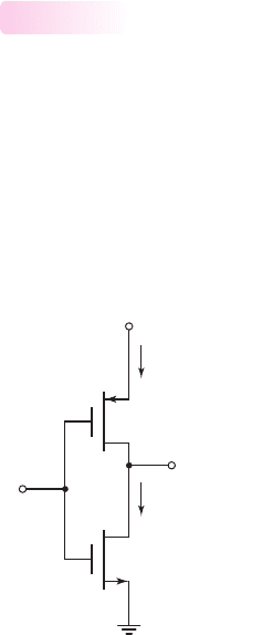
The CMOS inverter, shown in Figure 16.21, is a series combination of a p-channel
and an n-channel MOSFET. The gates of the two MOSFETs are connected together
to form the input and the two drains are connected together to form the output. Both
transistors are enhancement-mode devices. The parameters of the NMOS are de-
noted by
K
n
and
V
TN
, where
V
TN
> 0
, and the parameters of the PMOS are denoted
by
K
p
and
V
TP
, where
V
TP
< 0
.
16.3.2
i
DN
+
–
+
–
v
I
v
O
i
DP
V
DD
+
–
v
SDP
–
+
v
SGP
v
DSN
v
GSN
PMOS:
K
P
,V
TP
NMOS:
K
N
, V
T
N
Figure 16.21 CMOS inverter
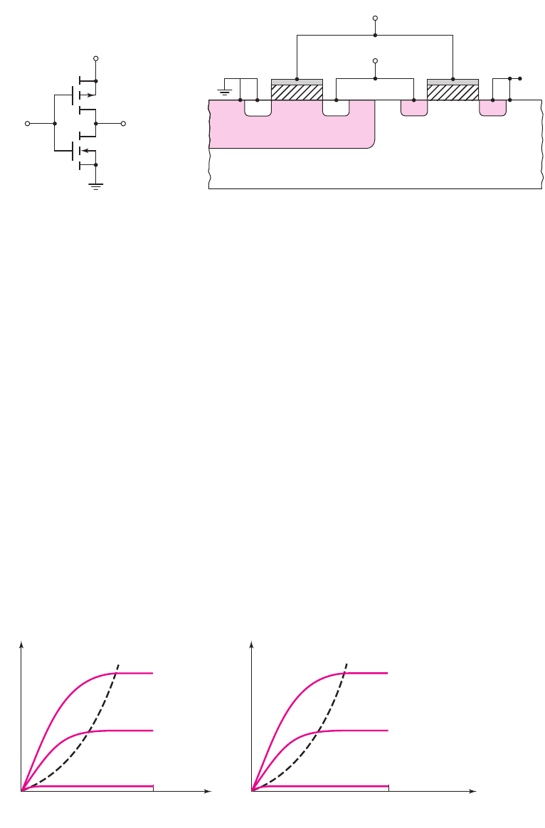
Figure 16.22 shows a simplified cross section of a CMOS inverter. In this
process, a separate p-well region is formed within the starting n-substrate. The
n-channel device is fabricated in the p-well region and the p-channel device is
fabricated in the n-substrate. Although other approaches, such as an n-well in a
p-substrate, are also used to fabricate CMOS circuits, the important point is that
the processing is more complicated for CMOS circuits than for NMOS circuits.
nea80644_ch16_1145-1254.qxd 07/12/2009 3:37 Page 1170 pinnacle MHDQ-New:MHDQ134:MHDQ134-16:
Chapter 16 MOSFET Digital Circuits 1171
However, the advantages of CMOS digital logic circuits over NMOS circuits justify
their use.
Voltage Transfer Curve
Figure 16.23 shows the transistor characteristics for both the n- and p-channel de-
vices. We can determine the voltage transfer characteristics of the inverter by evalu-
ating the various transistor bias regions. For
v
I
= 0
, the NMOS device is cut off,
i
DN
= 0
, and
i
DP
= 0
. The PMOS source-to-gate voltage is
V
DD
, which means that
the PMOS is biased on the curve marked B in Figure 16.23(b). Since the only
point on the curve corresponding to
i
DP
= 0
occurs at
v
SDP
= 0 = V
DD
−v
O
,the
output voltage is
v
O
= V
DD
. This condition exists as long as the NMOS transistor is
cut off, or
v
I
≤ V
TN
.
For
v
I
= V
DD
, the PMOS device is cut off,
i
DP
= 0
, and
i
DN
= 0
. The NMOS
gate-to-source voltage is
V
DD
and the NMOS is biased on the curve marked A in
Figure 16.23(a). The only point on the curve corresponding to
i
DN
= 0
occurs at
v
DSN
= v
O
= 0
. The output voltage is zero as long as the PMOS transistor is cut off,
or
v
SGP
= V
DD
−v
I
≤|V
TP
|
. This means that the input voltage is in the range
V
DD
−|V
TP
|≤v
I
≤ V
DD
.
V
DD
S
D
D
S
OutputInput
p-channel
n-channel
Output
Input
n-substrate
p-well
n
+
n
+
V
DD
DDSS
p
+
p
+
(b)(a)
Figure 16.22 Simplified cross section, CMOS inverter
i
DN
v
DSN
(sat)
V
DD
v
DSN
= v
O
v
GSN
= V
DD
A
C
0
v
GSN
= V
TN
+
i
DP
v
SDP
(sat)
V
DD
v
SDP
= V
DD
– v
O
v
SGP
= V
DD
B
0
v
SGP
= |V
TP
|
+
(a) (b)
Figure 16.23 Current–voltage characteristics, (a) NMOS transistor and (b) PMOS transistor
nea80644_ch16_1145-1254.qxd 07/12/2009 3:37 Page 1171 pinnacle MHDQ-New:MHDQ134:MHDQ134-16:
1172 Part 3 Digital Electronics
Figure 16.24 shows the voltage transfer characteristics generated thus far for
the CMOS inverter. The more positive output voltage corresponds to a logic 1,
or
V
OH
= V
DD
, and the more negative output voltage corresponds to a logic 0, or
V
OL
= 0
. When the output is in the logic 1 state, the NMOS transistor is cut off;
when the output is in the logic 0 state, the PMOS transistor is cut off.
Ideally, the current in the CMOS inverter in either steady-state condition is zero,
which means that, ideally, the quiescent power dissipation is zero. This result is the at-
tractive feature of CMOS digital circuits. In actuality, CMOS inverter circuits exhibit a
small leakage current in both steady-state conditions, due to the reverse-biased pn junc-
tions. However, the power dissipation may be in the nanowatt range rather than in the
milliwatt range of NMOS inverters. Without this feature, VLSI would not be possible.
When the input voltage is just greater than
V
TN
,or
v
I
= v
GSN
= V
+
TN
the NMOS begins to conduct and the Q-point falls on the curve marked C in
Figure 16.23(a). The current is small and
v
DSN
∼
=
V
DD
, which means that the NMOS
is biased in the saturation region. The PMOS source-to-drain voltage is small, so the
PMOS is biased in the nonsaturation region. Setting
i
DN
= i
DP
, we can write
K
n
[v
GSN
− V
TN
]
2
= K
p
2(v
SGP
+ V
TP
)v
SDP
−v
2
SDP
(16.34)
Relating the gate-to-source and drain-to-source voltages in each transistor to the inverter
input and output voltages, respectively, we can rewrite Equation (16.34) as follows:
K
n
[v
I
− V
TN
]
2
= K
p
[2(V
DD
−v
I
+ V
TP
)(V
DD
−v
O
) − (V
DD
−v
O
)
2
]
(16.35)
Equation (16.35) relates the input and output voltages as long as the NMOS is biased
in the saturation region and the PMOS is biased in the nonsaturation region.
The transition point for the PMOS is defined from
v
SDP
(sat) = v
SGP
+ V
TP
(16.36)
Using Figure 16.25, Equation (16.36) can be written
V
DD
− V
OPt
= V
DD
− V
IPt
+ V
TP
(16.37(a))
or
V
OPt
= V
IPt
− V
TP
(16.37(b))
V
OH
= V
DD
V
OL
= 0
v
O
v
I
V
TN
V
DD
(V
DD
– |V
TP
|)
0
PMOS cutoff
NMOS cutoff
Figure 16.24 CMOS inverter output voltage for input voltage in either high state or low state
nea80644_ch16_1145-1254.qxd 07/12/2009 3:37 Page 1172 pinnacle MHDQ-New:MHDQ134:MHDQ134-16:
Chapter 16 MOSFET Digital Circuits 1173
where
V
OPt
and
V
IPt
are the PMOS output and input voltages, respectively, at the
transition point.
The transition point for the NMOS is defined from
v
DSN
(sat) = v
GSN
− V
TN
(16.38(a))
or
V
ONt
= V
INt
− V
TN
(16.38(b))
where
V
ONt
and
V
INt
are the NMOS output and input voltages, respectively, at the
transition point.
On the basis that
V
TP
is negative for an enhancement-mode PMOS, Equa-
tions (16.37(b)) and (16.38(b)) are plotted in Figure 16.25. We determine the input
voltage at the transition points by setting the two drain currents equal to each other
when both transistors are biased in the saturation region. The result is
K
n
(v
GSN
− V
TN
)
2
= K
p
(v
SGP
+ V
TP
)
2
(16.39)
With the gate-to-source voltages related to the input voltage, Equation (16.39) becomes
K
n
(v
I
− V
TN
)
2
= K
p
(V
DD
−v
I
+ V
TP
)
2
(16.40)
For this ideal case, the output voltage does not appear in Equation (16.40), and the input
voltage is a constant, as long as the two transistors are biased in the saturation region.
Voltage
v
I
from Equation (16.40) is the input voltage at the PMOS and NMOS
transition points. Solving for
v
I
, we find that
v
I
= v
It
=
V
DD
+ V
TP
+
K
n
K
p
V
TN
1 +
K
n
K
p
(16.41)
For
v
I
> V
It
, the NMOS is biased in the nonsaturation region and the PMOS is
biased in the saturation region. Again equating the two drain currents, we have
K
n
2(v
GSN
− V
TN
)v
DSN
−v
2
DSN
= K
p
(v
SGP
+ V
TP
)
2
(16.42)
V
DD
v
O
v
I
V
TN
V
DD
A
B
C
(V
DD
– |V
TP
|)
V
ONt
= V
INt
– V
TN
V
OPt
= V
IPt
+ |V
TP
|
Transition point locus
for PMOS
Transition point locus
for NMOS
|V
TP
|
Figure 16.25 Regions of the CMOS transfer characteristics indicating NMOS and PMOS
transistor bias conditions. The NMOS device is biased in the saturation region in areas A
and B and in the nonsaturation region in area C. The PMOS device is biased in the saturation
region in areas B and C and in the nonsaturation region in area A.
nea80644_ch16_1145-1254.qxd 07/12/2009 3:37 Page 1173 pinnacle MHDQ-New:MHDQ134:MHDQ134-16:

1174 Part 3 Digital Electronics
Also, relating the gate-to-source and drain-to-source voltages to the input and output
voltages, respectively, modifies Equation (16.42) as follows:
K
n
2(v
I
− V
TN
)v
O
−v
2
O
= K
p
(V
DD
−v
I
+ V
TP
)
2
(16.43)
Equation (16.43) relates the input and output voltages as long as the NMOS
is biased in the nonsaturation region and the PMOS in the saturation region.
Figure 16.26 shows the complete voltage transfer curve.
EXAMPLE 16.7
Objective: Determine the critical voltages on the voltage transfer curve of a CMOS
inverter.
Consider a CMOS inverter biased at
V
DD
= 5V
with transistor parameters
K
n
= K
p
and
V
TN
=−V
TP
= 0.8
V. Then consider another CMOS inverter biased
at
V
DD
= 3V
with transistor parameters
K
n
= K
p
and
V
TN
=−V
TP
= 0.6
V.
Solution (V
DD
= 5 V): The input voltage at the transition points is, from Equa-
tion (16.41),
V
It
=
5 + (−0.8) +
√
1(0.8)
1 +
√
1
= 2.5V
The output voltage at the transition point for the PMOS is, from Equation
(16.37(b)),
V
OPt
= V
It
− V
TP
= 2.5 −(−0.8) = 3.2V
and the output voltage at the transition point or the NMOS is, from Equa-
tion (16.38(b)),
V
ONt
= V
It
− V
TN
= 2.5 −0.8 = 1.7V
Solution (V
DD
= 3 V): The critical voltages are
V
It
= 1.5V V
OPt
= 2.1V V
ONt
= 0.9V
v
O
v
I
V
OPt
V
DD
V
TN
V
It
V
DD
V
ONt
V
DD
– |V
TP
|
0
Figure 16.26 Complete voltage transfer characteristics, CMOS inverter
nea80644_ch16_1145-1254.qxd 07/12/2009 3:37 Page 1174 pinnacle MHDQ-New:MHDQ134:MHDQ134-16:
Chapter 16 MOSFET Digital Circuits 1175
Comment:
The two voltage transfer curves are shown in Figure 16.27. These figures
depict another advantage of CMOS technology, that is CMOS circuits can be biased
over a relatively wide range of voltages.
EXERCISE PROBLEM
Ex 16.7: The CMOS inverter in Figure 16.21 is biased at
V
DD
= 2.1V
, and the
transistor threshold voltages are
V
TN
=−V
TP
= 0.4
V. Sketch the voltage trans-
fer curve and show the critical voltages as in Figure 16.26 for (a)
K
n
/K
p
= 1
,
(b)
K
n
/K
p
= 0.5
, and (c)
K
n
/K
p
= 2
. (Ans. (a)
V
It
= 1.05 V
,
V
OPt
= 1.45 V
,
V
ONt
= 0.65 V
; (b)
V
It
= 1.16 V
,
V
OPt
= 1.56 V
,
V
ONt
= 0.76 V
; (c)
V
It
=
0.938 V
,
V
OPt
= 1.338 V
,
V
ONt
= 0.538 V
)
Transistor Sizing
We may note that both voltage transfer curves shown in Figure 16.27 are symmetri-
cal about the switching point
V
DD
/2
. This effect is a direct consequence of the fact
that the NMOS and PMOS transistors are matched: that is,
K
n
= K
p
and
V
TN
=
|
V
TP
|
. In general, the process conduction parameters,
k
n
and
k
p
, are not
equal. Therefore, in order for the two transistors to be matched, we must adjust the
width-to-length ratios. In order for
K
n
= K
p
, we have
k
n
(W/L)
n
= k
p
(W/L)
p
. In
general,
k
p
< k
n
, so we must have
(W/L)
p
>(WL)
n
. The PMOS device must be
larger than the NMOS device to make the two devices electrically equivalent.
CMOS Inverter Currents
When the CMOS inverter input voltage is either a logic 0 or a logic 1, the current in
the circuit is zero, since one of the transistors is cut off. When the input voltage is in
5
3
2.1
0.9
v
O
(V)
v
I
(V)
3.2
1.7
0 0.8 2.5 4.2 0.6 1.5 2.4 35
v
O
(V)
v
I
(V)
(a) (b)
Figure 16.27 Voltage transfer characteristics of CMOS inverter in Example 16.7 biased at
(a)
V
DD
= 5V
and (b)
V
DD
= 3V
nea80644_ch16_1145-1254.qxd 07/12/2009 3:37 Page 1175 pinnacle MHDQ-New:MHDQ134:MHDQ134-16:
1176 Part 3 Digital Electronics
the range
V
TN
<v
I
< V
DD
−|V
TP
|
, both transistors are conducting and a current
exists in the inverter.
When the NMOS transistor is biased in the saturation region, the current in the
inverter is controlled by
v
GSN
and the PMOS source-to-drain voltage adjusts such
that
i
DP
= i
DN
. This condition is demonstrated in Equation (16.34). We can write
i
DN
= i
DP
= K
n
(v
GSN
− V
TN
)
2
= K
n
(v
I
− V
TN
)
2
(16.44(a))
Taking the square root yields
i
DN
=
i
DP
=
K
n
(v
I
− V
TN
)
(16.44(b))
As long as the NMOS transistor is biased in the saturation region, the square root of
the CMOS inverter current is a linear function of the input voltage.
When the PMOS transistor is biased in the saturation region, the current in the
inverter is controlled by
v
SGP
and the NMOS drain-to-source voltage adjusts such
that
i
DP
= i
DN
. This condition is demonstrated in Equation (16.42). Using Equa-
tion (16.43), we can write that
i
DN
= i
DP
= K
p
(V
DD
−v
I
+ V
TP
)
2
(16.45(a))
Taking the square root yields
i
DN
=
i
DP
=
K
p
(V
DD
−v
I
+ V
TP
)
(16.45(b))
As long as the PMOS transistor is biased in the saturation region, the square root of
the CMOS inverter current is also a linear function of the input voltage.
Figure 16.28 shows plots of the square root of the inverter current for two values
of
V
DD
bias. These curves are quasi-static characteristics in that no current is diverted
into a capacitive load. At the inverter switching point, both transistors are biased in
the saturation region and both transistors influence the current. At the switching point,
the actual current characteristic does not have a sharp discontinuity in the slope. The
channel length modulation parameter
λ
also influences the current characteristics at
the peak value. However, the curves in Figure 16.28 are excellent approximations.
Power Dissipation
In the quiescent or static state, in which the input is either a logic 0 or a logic 1, power
dissipation in the CMOS inverter is virtually zero. However, during the switching
cycle from one state to another, current flows and power is dissipated. The CMOS
16.3.3
i
L
+
–
v
O
C
L
V
DD
v
SD
i
L
v
O
C
L
V
DD
(a) (b)
Figure 16.29 CMOS inverter when the output switches
(a) low to high and (b) high to low
0 0.6
0.8
2.5
1.5 2.4 3 4.2 5
v
I
(V)
i
DN
= i
DP
Figure 16.28 Square root of CMOS inverter current versus
input voltage for CMOS inverters described in Example 16.7
nea80644_ch16_1145-1254.qxd 07/12/2009 3:37 Page 1176 pinnacle MHDQ-New:MHDQ134:MHDQ134-16:

Chapter 16 MOSFET Digital Circuits 1177
inverter and logic circuits are used to drive other MOS devices for which the input
impedance is a capacitance. During the switching cycle, then, this load capacitance
must be charged and discharged.
In Figure 16.29(a), the output switches from its low to its high state. The input is
switched low, the PMOS gate is at zero volts, and the NMOS is cut off. The load ca-
pacitance
C
L
must be charged through the PMOS device. Power dissipation in the
PMOS transistor is given by
P
P
= i
L
v
SD
= i
L
(V
DD
−v
O
)
(16.46)
The current and the output voltage are related by
i
L
= C
L
dv
O
dt
(16.47)
The energy dissipated in the PMOS device as the output switches from low to
high is
E
P
=
∞
0
P
P
dt =
∞
0
C
L
(V
DD
−v
O
)
dv
O
dt
dt
= C
L
V
DD
V
DD
0
dv
O
−C
L
V
DD
0
v
O
dv
O
(16.48)
which yields
E
P
= C
L
V
DD
v
O
V
DD
0
−C
L
v
2
O
2
V
DD
0
=
1
2
C
L
V
2
DD
(16.49)
After the output has switched high, the energy stored in the load capacitance is
(
1
2
)C
L
V
2
DD
. When the inverter input goes high, the output switches low, as shown in
Figure 16.29(b). The PMOS device is cut off, the NMOS transistor conducts, and the
load capacitance discharges through the NMOS device. All the energy stored in
the load capacitance is dissipated in the NMOS device. As the output switches from
high to low, the energy dissipated in the NMOS transistor is
E
N
=
1
2
C
L
V
2
DD
(16.50)
The total energy dissipated in the inverter during one switching cycle is therefore
E
T
= E
P
+ E
N
=
1
2
C
L
V
2
DD
+
1
2
C
L
V
2
DD
= C
L
V
2
DD
(16.51)
If the inverter is switched at frequency f, the power dissipated in the inverter is
P = fE
T
= fC
L
V
2
DD
(16.52)
Equation (16.52) shows that the power dissipated in a CMOS inverter is directly pro-
portional to the switching frequency and to
V
2
DD
. The drive in digital IC design is
toward lower supply voltages, such as 3 V or less.
The power dissipation is proportional to
V
2
DD
. In some digital circuits, such as
digital watches, the CMOS logic circuits are biased at
V
DD
= 1.5V
, so the power
dissipation is substantially reduced.
EXAMPLE 16.8
Objective: Calculate the power dissipation in a CMOS inverter.
Consider a CMOS inverter with a load capacitance of
C
L
= 2pF
biased at
V
DD
= 5V
. The inverter switches at a frequency of
f = 100 kHz
.
nea80644_ch16_1145-1254.qxd 07/12/2009 3:37 Page 1177 pinnacle MHDQ-New:MHDQ134:MHDQ134-16: