Neamen D. Microelectronics: Circuit Analysis and Design
Подождите немного. Документ загружается.

1148 Part 3 Digital Electronics
16.1 NMOS INVERTERS
Objective: • Analyze and design NMOS inverters.
The inverter is the basic circuit of most MOS logic circuits. The design techniques
used in NMOS logic circuits are developed from the dc analysis results for the
NMOS inverter. Extending the concepts developed from the inverter to NOR and
NAND gates is then direct. Alternative inverter load elements are compared in terms
of power consumption, packing density, and transfer characteristics.
n-Channel MOSFET Revisited
We studied the structure, operation, and characteristics of MOS transistors in
Chapter 3. In this section, we will quickly review the n-channel MOSFET character-
istics, emphasizing specific properties important in digital circuit design.
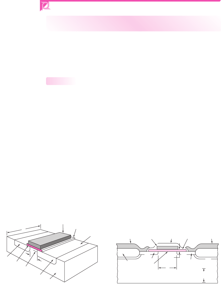
The simplified n-channel MOSFET that we have considered is shown in Figure
16.1(a). A more detailed view of the n-channel MOSFET is shown in Figure 16.1(b).
The active transistor region is the surface of the semiconductor and comprises heav-
ily doped n
source and drain regions and the p-type channel region. The channel
length is L and the channel width is W. The body, or substrate, is a single-crystal sil-
icon wafer, which is the starting material for circuit fabrication and provides physi-
cal support for the integrated circuit.
In an integrated circuit, all n-channel transistors are fabricated in the same
p-type substrate material. The substrate is connected to the most negative potential in
the circuit, which for digital circuits is normally at ground potential or zero volts.
However, the source terminal of many transistors will not be at zero volts, which
means that a reverse-biased pn junction will exist between the source and substrate.
When the source and body terminals are not at the same potential, the threshold volt-
age of the transistor becomes a function of the source-to-body voltage. This body
effect must then be taken into account in determining logic levels in digital circuits.
16.1.1
n
+
-type
semiconductor
n
+
-source
n
+
-drain
p-substrate
L
W
Polysilicon
or metal
Oxide
Gate
Channel
region
(a) (b)
L
Channel length L
p-type body, B
SiO
2
SiO
2
t
ox
Gate
dielectric
(silicon
dioxide)
Field
oxide
Drain
1 mm vertical
scale
Metal source
contact, S
Deposited
insulator
Gate, G
n-type
polysilicon
Metal drain
contact, D
n
+
n
+
Source
Channel
region
p
+
Figure 16.1 (a) n-channel MOSFET simplified view and (b) n-channel MOSFET detailed
cross section
nea80644_ch16_1145-1254.qxd 07/12/2009 3:37 Page 1148 pinnacle MHDQ-New:MHDQ134:MHDQ134-16:
Chapter 16 MOSFET Digital Circuits 1149
Current–Voltage Relation
The current–voltage characteristics of the n-channel MOSFET are functions of both
the electrical and geometric properties of the device. When the transistor is biased in
the nonsaturation region, for
v
GS
≥ V
TN
and
v
DS
≤ (v
GS
− V
TN
)
, we can write
i
D
= K
n
2(v
GS
− V
TN
)v
DS
−v
2
DS
(16.1(a))
In the saturation region, for
v
GS
≥ V
TN
and
v
DS
≥ (v
GS
− V
TN
)
, we have
i
D
= K
n
(v
GS
− V
TN
)
2
(16.1(b))
The transition point separates the nonsaturation and saturation regions and is the
drain-to-source saturation voltage, which is given by
v
DS
= v
DS
(sat) = v
GS
− V
TN
(16.2)
The term
(1 + λv
DS
)
is sometimes included in Equation (16.1(b)) to account for
channel length modulation and the finite output resistance. In most cases, it has little
effect on the operating characteristics of MOS digital circuits. In our analysis, the
term
λ
is assumed to be zero unless otherwise stated.
The parameter
K
n
is the NMOS transistor conduction parameter and is given by
K
n
=
1
2
μ
n
C
ox
W
L
=
k
n
2
W
L
(16.3)
The electron mobility
μ
n
and oxide capacitance
C
ox
are assumed to be constant for
all devices in a particular IC.
The current–voltage characteristics are directly related to the channel width-to-
length ratio, or the size of the transistor. In general, in a given IC, the length L is
fixed, but the designer can control the channel width W.
Since the MOS transistor is a majority carrier device, the switching speed of
MOS digital circuits is limited by the time required to charge and discharge the ca-
pacitances between device electrodes and between interconnect lines and ground.
Figure 16.2 shows the significant capacitances in a MOSFET. The capacitances
C
sb
and
C
db
are the source-to-body and drain-to-body n
+
p junction capacitances. The
total input gate capacitance, to a first approximation, is a constant equal to
C
g
= WLC
ox
= WL
ε
ox
t
ox
(16.4)
where
C
ox
is the oxide capacitance per unit area, and is a function of the oxide thick-
ness. The parameter
C
ox
also appears in the expression for the conduction parameter.
C
gd
C
db
C
gs
C
g
b
D
G
B
S
C
sb
Figure 16.2 n-channel MOSFET and device capacitances
nea80644_ch16_1145-1254.qxd 07/12/2009 3:37 Page 1149 pinnacle MHDQ-New:MHDQ134:MHDQ134-16:
1150 Part 3 Digital Electronics
Small Geometry Effects
The current–voltage relationships given by Equations (16.1(a)), (16.1(b)), and (16.2)
are first-order approximations that apply to “long” channel devices. The tendency in
device design is to make the devices as small as possible, which means the channel
length is being reduced to values substantially smaller than 1 μm. The corresponding
channel widths are also being reduced. As the channel length is reduced, several ef-
fects alter the current–voltage characteristics. First, the threshold voltage becomes a
function of the geometry of the device and is dependent on the channel length. This
effect must be taken into account in the design of the transistor. Second, carrier
velocity saturation reduces the saturation-mode current below the current value pre-
dicted by Equation (16.1(b)). The current is no longer a quadratic function of gate-
to-source voltage, and tends to become a linear function of voltage. Channel length
modulation means that the current tends to be larger than that predicted by the ideal
equation. Third, the electron mobility is a function of the gate voltage so that the cur-
rent tends to be smaller than the predicted value as the gate-to-source voltage in-
creases. All of these effects complicate the analysis considerably.
We can, however, determine the basic operation and behavior of MOSFET logic
circuits by using the first-order equations. We will use these first-order equations in
our design of logic circuits. To determine the effect of small device size, a computer
simulation may be performed in which the appropriate device models are incorpo-
rated in the simulation.
NMOS Inverter Transfer Characteristics
Since the inverter is the basis for most logic circuits, we will describe the NMOS
inverter and will develop the dc transfer characteristics for three types of inverters
with different load devices. This discussion will introduce voltage transfer functions
and will define the maximum and minimum logic levels.
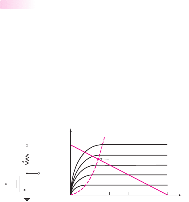
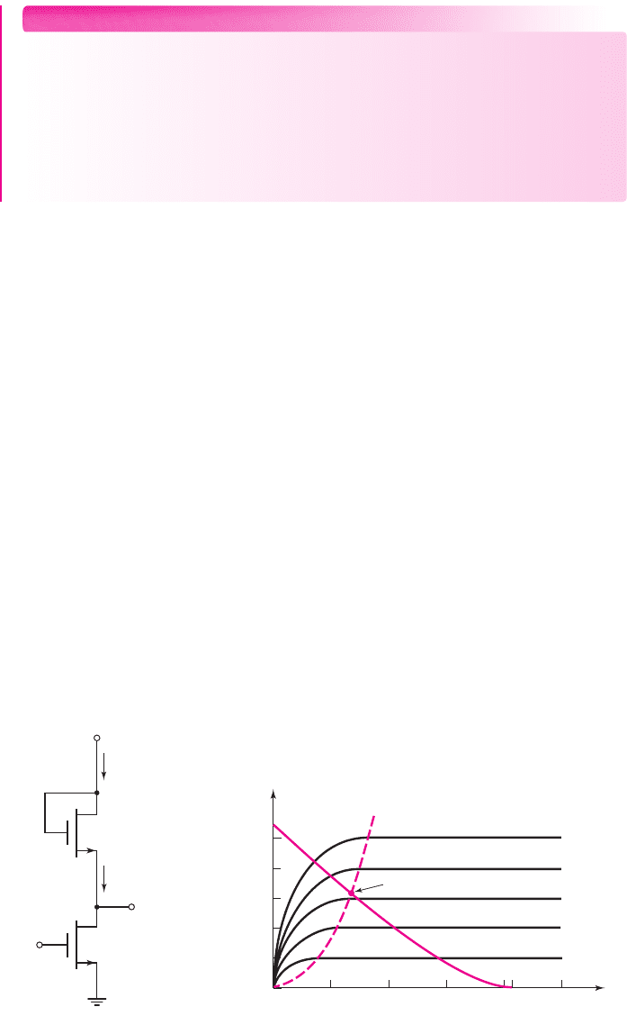
NMOS Inverter with Resistor Load
Figure 16.3(a) shows a single NMOS transistor connected to a resistor to form an
inverter. The transistor characteristics and load line are shown in Figure 16.3(b),
along with the parametric curve separating the saturation and nonsaturation regions.
We determine the voltage transfer characteristics of the inverter by examining the
various regions in which the transistor can be biased.
When the input voltage is less than or equal to the threshold voltage, or
v
I
≤ V
TN
, the transistor is cut off,
i
D
= 0
, and the output voltage is
v
O
= V
DD
. The
maximum output voltage is defined as the logic 1 level. As the input voltage becomes
16.1.2
i
D
V
DD
R
D
v
O
v
I
i
D
v
DS
(sat) = v
GS
– V
TN
v
DS
V
DD
V
DD
R
D
Transition point
Figure 16.3 (a) NMOS inverter with resistor load and (b) transistor characteristics and load line
nea80644_ch16_1145-1254.qxd 07/12/2009 3:37 Page 1150 pinnacle MHDQ-New:MHDQ134:MHDQ134-16:
Chapter 16 MOSFET Digital Circuits 1151
just greater than
V
TN
, the transistor turns on and is biased in the saturation region.
The output voltage is then
v
O
= V
DD
−i
D
R
D
(16.5)
where the drain current is given by
i
D
= K
n
(v
GS
− V
TN
)
2
= K
n
(v
I
− V
TN
)
2
(16.6)
Combining Equations (16.5) and (16.6) yields
v
O
= V
DD
− K
n
R
D
(v
I
− V
TN
)
2
(16.7)
which relates the output and input voltages as long as the transistor is biased in the
saturation region.
As the input voltage increases, the Q-point of the transistor moves up the load
line. At the transition point, we have
V
Ot
= V
It
− V
TN
(16.8)
where
V
Ot
and
V
It
are the drain-to-source and gate-to-source voltages, respectively,
at the transition point. Substituting Equation (16.8) into (16.7), we determine the
input voltage at the transition point from
K
n
R
D
(V
It
− V
TN
)
2
+(V
It
− V
TN
) − V
DD
= 0
(16.9)
As the input voltage becomes greater than
V
It
, the Q-point continues to move up
the load line, and the transistor becomes biased in the nonsaturation region. The drain
current is then
i
D
= K
n
2(v
GS
− V
TN
)v
DS
−v
2
DS
= K
n
2(v
I
−v
TN
)v
O
−v
2
O
(16.10)
Combining Equations (16.5) and (16.10) yields
v
O
= V
DD
− K
n
R
D
2(v
I
− V
TN
)v
O
−v
2
O
(16.11)
which relates the input and output voltages as long as the transistor is biased in the
nonsaturation region.
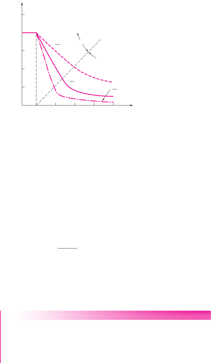
Figure 16.4 shows the voltage transfer characteristics of this inverter for three re-
sistor values. Also shown is the line, given by Equation (16.8), which separates the
v
O
(V)
V
DD
= 2.5
v
I
(V)
0.5
1.0
1.5
2.0
0 0.5 1.0 1.5 2.0 2.5
V
Ot
= V
It
– V
TN
Saturation
Nonsaturation
R
D
= 50 kΩ
R
D
= 25 kΩ
R
D
= 5 kΩ
Cutoff
Figure 16.4 Voltage transfer characteristics of NMOS inverter with resistive load, using
parameters from Example 16.1 and for the three resistor values.
nea80644_ch16_1145-1254.qxd 07/12/2009 3:37 Page 1151 pinnacle MHDQ-New:MHDQ134:MHDQ134-16:

1152 Part 3 Digital Electronics
saturation and nonsaturation bias regions of the transistor. The figure shows that
the minimum output voltage, or the logic 0 level, for a high input decreases with in-
creasing load resistance, and the sharpness of the transition region between a low
input and a high input increases with increasing load resistance.
It should be noted that a large resistance is difficult to fabricate in an IC. A
large resistor value in the inverter will limit current and power consumption as
well as provide a small
V
OL
value. But it would also require a large chip area if
fabricated in a standard MOS process. To avoid this problem MOS transistors
can be used as load devices, replacing the resistor, as discussed in subsequent
paragraphs.
EXAMPLE 16.1
Objective: Determine the transition point, minimum output voltage, maximum
drain current, and maximum power dissipation of an NMOS inverter with resistor
load.
Specifications: Consider the circuit in Figure 16.3(a) with parameters
V
DD
= 2.5V
and
R
D
= 20 k
. The transistor parameters are
V
TN
= 0.5V
and
K
n
= 0.3mA/V
2
.
Solution: The input voltage at the transition point is found from Equation (16.9).
We have
(0.3)(25)(V
It
−0.5)
2
+(V
It
−0.5) − 2.5 = 0
which yields
V
It
−0.5 = 0.515
Vor
V
It
= 1.015
V
The output voltage at the transition point is
V
Ot
= V
It
− V
TN
= 1.015 −0.5 = 0.515 V
When
v
I
is high at
v
I
= 2.5V
, the output voltage is found from Equation (16.11).
We find
v
O
= 2.5 −(0.3(25)[2(2.5 − 0.5)v
O
−v
2
O
]
which yields the output low level as
v
O
= V
OL
= 82.3
mV
The maximum drain current in the inverter occurs when
v
O
= V
OL
and is found to be
i
D,max
=
2.5 − 0.0823
25
⇒ 96.7 μA
The maximum power dissipated in the inverter is
P
D,max
= i
D,max
· V
DD
= (0.0967)(2.5) = 0.242 mW
Comment: The level of
V
OL
is less than the threshold voltage
V
TN
; therefore, if
the output of this inverter is used to drive a similar inverter, the driver transistor of the
load inverter would be cut off and its output would be high, which is the desired
condition. We will compare the maximum drain currents and maximum power dissi-
pations of the three basic NMOS inverters.
nea80644_ch16_1145-1254.qxd 07/12/2009 3:37 Page 1152 pinnacle MHDQ-New:MHDQ134:MHDQ134-16:
Chapter 16 MOSFET Digital Circuits 1153
EXERCISE PROBLEM
Ex 16.1: Consider the NMOS inverter with resistor load in Figure 16.3(a) biased at
V
DD
= 3
V. Assume transistor parameters of
k
n
= 100 μ
A/V
2
,
W/L = 4
,and
V
TN
= 0.5
V. (a) Find the value of
R
D
such that
v
O
= 0.1V
when
v
I
= 3
V.
(b) Using the results of part (a), determine the maximum current and maximum
power dissipation in the inverter. (c) Using the results of part (a), determine the
transition point for the driver transistor. (Ans. (a)
R
D
= 29.6
k
; (b)
i
D,max
=
0.098
mA,
P
D,max
= 0.294
mW; (c)
V
It
= 1.132
V,
V
Ot
= 0.632
V)
i
D
v
DS
(sat) = v
GS
– V
TN
v
DS
V
DD
V
DD
– V
TNL
Transition point
(a) (b)
i
DD
+
–
+
–
v
I
v
O
i
DL
V
DD
+
–
v
DSL
+
–
v
GSL
v
DSD
v
GSD
Load:
V
TNL
, K
L
Driver:
V
TND
, K
D
Figure 16.5 (a) NMOS inverter with saturated load and (b) driver transistor characteristics
and load curve
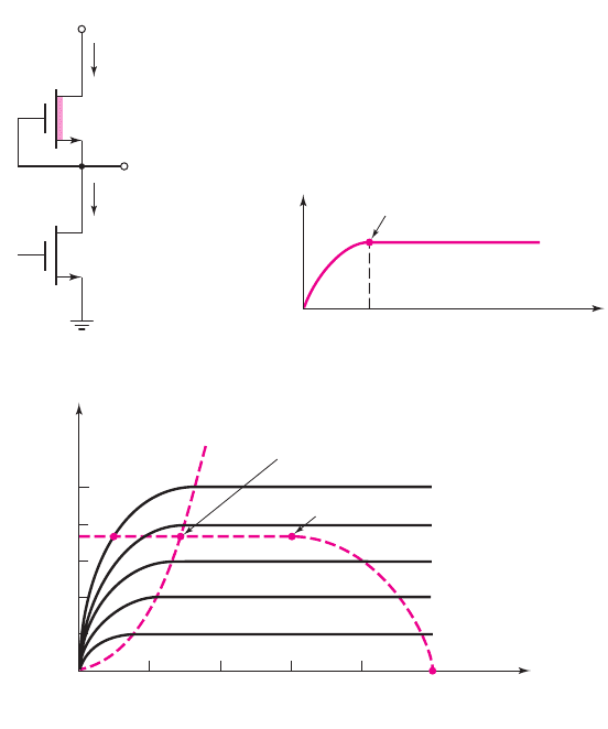
An n-channel enhancement-mode MOSFET with the gate connected to the drain can
be used as a load device in an NMOS inverter. This device configuration was ana-
lyzed in Chapter 3. We found that, when
v
GS
= v
DS
≥ V
TN
, the transistor always
operates in the saturation region. The drain current is given by
i
D
= K
n
(v
GS
− V
TN
)
2
= K
n
(v
DS
− V
TN
)
2
(16.12)
We continue to neglect the effect of the output resistance and the
λ
parameter.
Figure 16.5(a) shows an NMOS inverter with the enhancement load device. The
driver transistor parameters are denoted by
V
TND
and
K
D
, and the load transistor pa-
rameters are denoted by
V
TNL
and
K
L
. The substrate connections are not shown. In
the following analysis, we neglect the body effect and we assume all threshold volt-
ages are constant. These assumptions do not seriously affect the basic analysis, nor
the inverter characteristics.
The driver transistor characteristics and the load curve are shown in Figure 16.5(b).
When the inverter input voltage is less than the driver threshold voltage, the driver is
cut off and the drain currents are zero. From Equation (16.12), we have
i
DL
= 0 = K
L
(v
DSL
− V
TNL
)
2
(16.13)
nea80644_ch16_1145-1254.qxd 07/12/2009 3:37 Page 1153 pinnacle MHDQ-New:MHDQ134:MHDQ134-16:

1154 Part 3 Digital Electronics
From Figure 16.5(a), we see that
v
DSL
= V
DD
−v
O
, which means that
v
DSL
− V
TNL
= V
DD
−v
O
− V
TNL
= 0
(16.14(a))
The maximum output voltage is then
v
O,max
≡ V
OH
= V
DD
− V
TNL
(16.14(b))
For the enhancement-load NMOS inverter, the maximum output voltage, which is
the logic 1 level, does not reach the full
V
DD
value. This cutoff point is shown in the
load curve in Figure 16.5(b).
As the input voltage becomes just greater than the driver threshold voltage
V
TND
, the driver transistor turns on and is biased in the saturation region. In
steady-state, the two drain currents are equal since the output will be connected to the
gates of other MOS transistors. We have
i
DD
= i
DL
, which can be written as
K
D
(v
GSD
− V
TND
)
2
= K
L
(v
GSL
− V
TNL
)
2
(16.15)
Equation (16.15) is expressed in terms of the individual transistor parameters. In
terms of the input and output voltages, the expression becomes
K
D
(v
I
− V
TND
)
2
= K
L
(V
DD
−v
O
− V
TNL
)
2
(16.16)
Solving for the output voltage yields
v
O
= V
DD
− V
TNL
−
K
D
K
L
(v
I
− V
TND
)
(16.17)
As the input voltage increases, the driver Q-point moves up the load curve and
the output voltage decreases linearly with
v
I
.
At the driver transition point, we have
v
DSD
(sat) = v
GSD
− V
TND
or
V
Ot
= V
It
− V
TND
(16.18)
Substituting Equation (16.18) into (16.17), we find the input voltage at the transition
point, which is
V
It
=
V
DD
− V
TNL
+ V
TND
1 +
K
D
K
L
1 +
K
D
K
L
(16.19)
As the input voltage becomes greater than
V
It
, the driver transistor Q-point con-
tinues to move up the load curve and the driver becomes biased in the nonsaturation
region. Since the driver and load drain currents are still equal, or
i
DD
= i
DL
, we now
have
K
D
2(v
GSD
− V
TND
)v
DSD
−v
2
DSD
= K
L
(v
DSL
− V
TNL
)
2
(16.20)
Writing Equation (16.20) in terms of the input and output voltages produces
K
D
2(v
I
− V
TND
)v
O
−v
2
O
= K
L
(V
DD
−v
O
− V
TNL
)
2
(16.21)
Obviously, the relationship between
v
I
and
v
O
in this region is not linear.
nea80644_ch16_1145-1254.qxd 07/12/2009 3:37 Page 1154 pinnacle MHDQ-New:MHDQ134:MHDQ134-16:
Chapter 16 MOSFET Digital Circuits 1155
v
O
(V)
v
I
(V)
0.5
1.0
1.5
2.0
0 0.5 1.0 1.5 2.0 2.5
2.5
V
St
= V
It
– V
TND
= 1
Nonsaturation
Saturation
K
D
K
L
= 4
K
D
K
L
= 12.4
K
D
K
L
Figure 16.6 Voltage transfer characteristics of NMOS inverter with saturated
load, using parameters from Example 16.2 and for three aspect ratios.
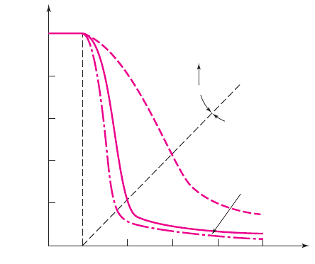
Figure 16.6 shows the voltage transfer characteristics of this inverter for three
K
D
-to-
K
L
ratios. The ratio
K
D
/K
L
is the aspect ratio and is related to the width-to-
length parameters of the driver and load transistors.
The line, given by Equation (16.18), separating the driver saturation and nonsat-
uration regions is also shown in the figure. We see that the minimum output voltage,
or the logic 0 level, for a high input decreases with an increasing
K
D
/K
L
ratio. As
the width-to-length ratio of the load transistor decreases, the effective resistance
increases, which means that the general behavior of the transfer characteristics is
the same as for the resistor load. However, the high output voltage is
V
OH
= V
DD
− V
TNL
When the driver is biased in the saturation region, we find the slope of the trans-
fer curve, which is the inverter gain, by taking the derivative of Equation (16.17)
with respect to
v
I
. We see that
dv
O
/dv
I
=−
K
D
/K
L
When the aspect ratio is greater than unity, the inverter gain magnitude is greater than
unity. A logic circuit family with an inverter transfer curve that exhibits a gain greater
than unity for some region is called a restoring logic family. Restoring logic is so
named because logic signals that are degraded for some reason in one circuit can be
restored by the gain of subsequent logic circuits.
DESIGN EXAMPLE 16.2
Objective: Design an NMOS inverter to meet a set of specifications and determine
the power dissipation in the inverter.
Specifications: The NMOS inverter with saturated load shown in Figure 16.5(a) is
to be designed such that
v
O
= 0.1
V when
v
I
= 2.0
V. The circuit is biased at
V
DD
= 2.5
V. (Neglect the body effect.)
nea80644_ch16_1145-1254.qxd 07/12/2009 3:37 Page 1155 pinnacle MHDQ-New:MHDQ134:MHDQ134-16:

1156 Part 3 Digital Electronics
Choices: Transistors are available with parameters
V
TN
= 0.5
V and
k
n
=
100 μ
A/V
2
.
Solution: The maximum output voltage (defined as a logic 1), neglecting the body
effect, is
V
OH
= V
DD
− V
TNL
= 2.5 −0.5 = 2.0V
For
v
I
= 2.0
V, the driver is biased in the nonsaturation region and the load is al-
ways biased in the saturation region. Setting the two drain currents equal to each
other, we find, using Equation (16.21),
K
D
[2(2.0 − 0.5)(0.1) − (0.1)
2
] = K
L
(2.5 − 0.1 −0.5)
2
which yields
K
D
K
L
= 12.4
If we choose
(W/L)
L
= 1
, and since
K
D
K
L
=
(W/L)
D
(W/L)
L
then we have
W
L
D
= 12.4
The maximum inverter current occurs for
v
O
= V
OL
= 0.1
V and is found from
i
D,max
=
k
n
2
·
W
L
D
2(v
I
− V
TND
)v
O
−v
2
O
=
0.1
2
(12.4)
2(2.0 − 0.5)(0.1) − (0.1)
2
= 0.180 mA
The maximum power dissipated in the inverter is
P
D,max
= i
D,max
· V
DD
= (0.18)(2.5) = 0.45 mW
Comment: In the NMOS inverter with enhancement-mode load, a relatively large
difference in sizes of the driver and load transistors is required to produce a relatively
low output voltage
V
OL
. The load transistor width-to-length ratio cannot be reduced
substantially, so the maximum power dissipation cannot be substantially reduced
from the 0.45 mW.
EXERCISE PROBLEM
Ex 16.2: The enhancement-load NMOS inverter in Figure 16.5(a) is biased
at
V
DD
= 3
V. The transistor parameters are
k
n
= 100 μ
A/V
2
,
V
TND
=
V
TNL
= 0.4
V,
(W/L)
D
= 16
, and
(W/L)
L
= 2
. (a) Determine
v
O
when
(i)
v
I
= 0.1
V and (ii)
v
I
= 2.6
V. Neglect the body effect. (b) Determine the max-
imum current and maximum power dissipation in the inverter. (c) Determine the
transition point for the driver transistor. (Ans. (a) (i)
v
O
= 2.6
V, (ii)
v
O
= 0.174
V;
(b)
i
D,max
= 0.589
mA,
P
D,max
= 1.766
mW; (c)
V
It
= 1.08
V,
V
Ot
= 0.68
V)
nea80644_ch16_1145-1254.qxd 07/12/2009 3:37 Page 1156 pinnacle MHDQ-New:MHDQ134:MHDQ134-16:
Chapter 16 MOSFET Digital Circuits 1157
NMOS Inverter with Depletion Load
Depletion-mode MOSFETs can also be used as load elements in NMOS inverters.
Figure 16.7(a) shows the NMOS inverter with depletion load. The gate and source
of the depletion-mode transistor are connected together. The driver transistor is
still an enhancement-mode device. As before, the driver transistor parameters are
V
TND
(V
TND
> 0)
and
K
D
, and the load transistor parameters are
V
TNL
(V
TNL
< 0)
and
K
L
. Again, the substrate connections are not shown. The fabrication process
for this inverter is slightly more complicated than for the enhancement-load in-
verter, since the threshold voltages of the two devices are not equal. However, as
we will see, the advantages of this inverter make the extra processing steps worth-
while. This inverter has been the basis of many microprocessor and static memory
designs.
The current–voltage characteristic curve for the depletion load, neglecting the
body effect, is shown in Figure 16.7(b). Since the gate is connected to the source,
v
GSL
= 0
, and the Q-point of the load is on this particular curve.
The driver transistor characteristics and the ideal load curve are shown in
Figure 16.7(c). When the inverter input is less than the driver threshold voltage, the
driver is cut off and the drain currents are zero. From Figure 16.7(b), we see that for
i
DD
+
–
+
–
v
I
v
O
i
DL
V
DD
+
–
v
DSD
v
GSD
Load:
V
TNL
, K
L
Driver:
V
TND
, K
D
v
DSL
i
DL
v
DS
L
v
DSL
(sat) = v
GSL
– V
TNL
= – V
TNL
v
GSL
= 0
i
D
v
DS
(sat) = v
GS
– V
TN
v
GSD
= V
DD
D
C
B
A
v
DS
V
DD
Transition point for load
Transition point for driver
Load curve
(a) (b)
(c)
Figure 16.7 (a) NMOS inverter with depletion load, (b) current–voltage characteristic of
depletion load, and (c) driver transistor characteristics and load curve
nea80644_ch16_1145-1254.qxd 07/12/2009 3:37 Page 1157 pinnacle MHDQ-New:MHDQ134:MHDQ134-16: