Neamen D. Microelectronics: Circuit Analysis and Design
Подождите немного. Документ загружается.

1218 Part 3 Digital Electronics
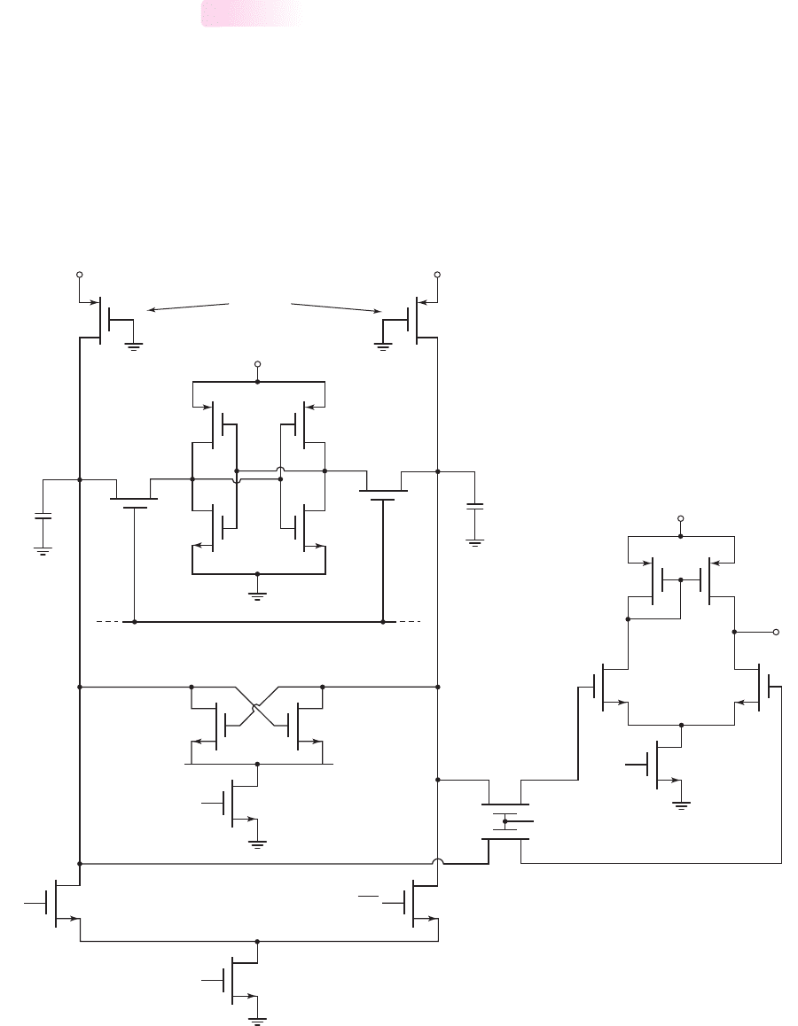
SRAM Read/Write Circuitry
An example of a read/write circuit at the end of a column is shown in Figure 16.79.
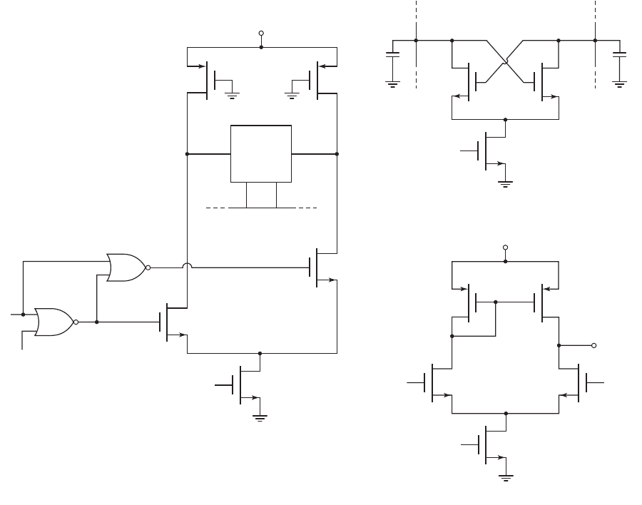
We may consider the write portion of the circuit as shown in Figure 16.80(a). We
may note that if the column is not selected, then
M
3
is cut off and the two data lines
are held at their precharged value of
V
DD
. When
X = Y = 1
, then the one-bit cell
shown is addressed. If
¯
W = 1
then the write cycle is deselected and both
M
1
and
M
2
are cut off. For
¯
W = 0
and
D = 1
,
M
1
is cut off and
M
2
is turned on so that the
¯
D
data line is pulled low while the D data line remains high. The logic 1 is then written
into the cell. For
¯
W = 0
and
D = 0
, the D data line is pulled low and the
¯
D
data line
is held high so that logic 0 is written into the cell.
16.9.3
Pull-up
transistors
Word line
CLK
CLK
Write
circuitry
Y
column
select
WBWB
Read
select
Sense
amplifier
M
P4
M
P3
DD
–
–
–
Q
Q
M
P1
M
A
M
B
M
P2
M
N2
M
N1
V
DD
V
DD
V
DD
V
O
V
DD
C
D
C
D
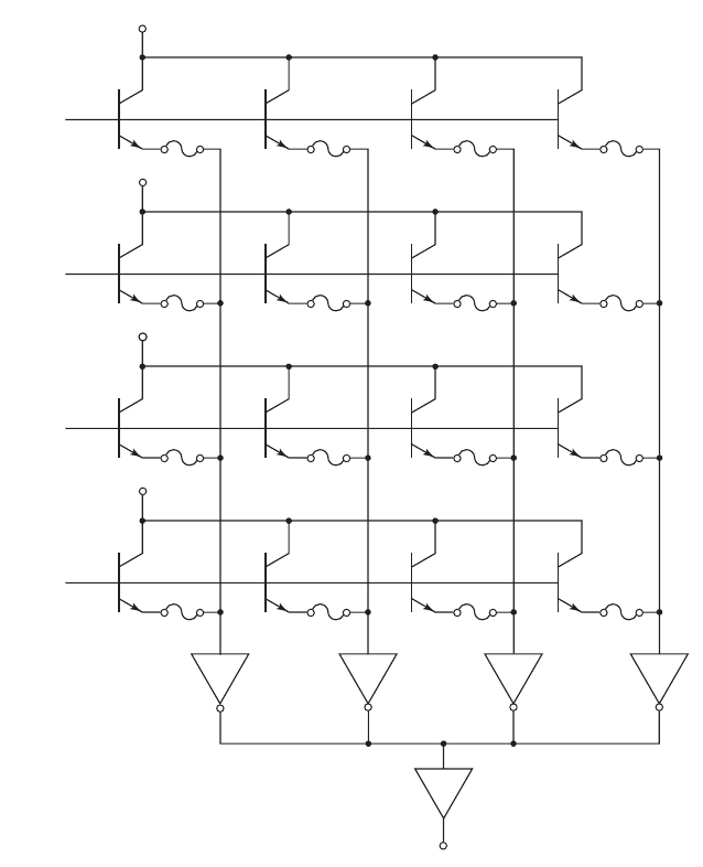
Figure 16.79 Complete circuit diagram of a CMOS RAM cell with write and read circuitry
nea80644_ch16_1145-1254.qxd 07/12/2009 3:38 Page 1218 pinnacle MHDQ-New:MHDQ134:MHDQ134-16:
Chapter 16 MOSFET Digital Circuits 1219
Figure 16.80(b) shows the NMOS cross-coupled sense amplifier that is in the
complete circuit of Figure 16.79. This circuit does not generate an output signal, but
rather amplifies the small difference in the data bit lines. Suppose that a logic 1 is to
be read from the memory cell. When the cell is addressed, the D bit line is high and
the
¯
D
bit line voltage begins to decrease. This means that when the
M
3
transistor
turns on, the
M
2
transistor turns on harder than
M
1
so that the
¯
D
bit line voltage is
pulled low and the
M
1
transistor will eventually turn off.
Figure 16.80(c) shows the differential amplifier that senses the output of the
memory cell. Note that this sense amplifier is connected to the bit lines through a
couple of pass transistors, as seen in Figure 16.79. If the input signal to the pass tran-
sistors is also a function of the column select signal, then this configuration enables
the use of one main sense amplifier to read the data out of several columns, one at a
time. When the clock signal is zero, the
M
3
transistor in the differential amplifier is
cut off and the common source node of
M
1
and
M
2
is pulled high, which means the
output voltage is pulled high. When a memory cell is selected and the clock goes
high,
M
3
turns on. If a logic 1 level is to be read, then D remains high and the
¯
D
line
X, word line
CLK
CLK
Data
CMOS
SRAM
cell
D
M
1
M
2
M
1
M
2
M
3
M
3
M
4
M
1
M
5
M
2
V
DD
–
D
D
–
D
–
C
D
C
D
V
O
V
DD
Y
column
select
W
–
(b)
(c)(a)
Figure 16.80 (a) Write circuitry associated with CMOS RAM cell; (b) cross-coupled NMOS
sense amplifier; (c) CMOS differential sense amplifier
nea80644_ch16_1145-1254.qxd 07/12/2009 3:38 Page 1219 pinnacle MHDQ-New:MHDQ134:MHDQ134-16:

1220 Part 3 Digital Electronics
Row select = WL
Data
line
C
S
M
S
C
B
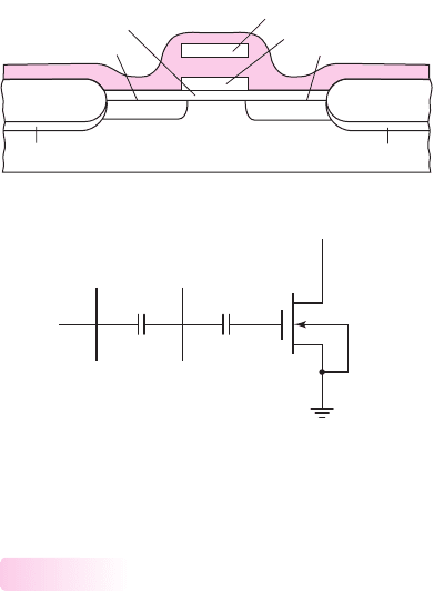
Figure 16.81 One-transistor dynamic RAM cell
voltage decreases. This means that the
M
2
transistor will turn off and the output volt-
age remains high. If a logic 0 is to be read, then the D line voltage decreases and
¯
D
remains high. The transistor
M
1
will turn off while
M
2
is turned on so that the output
voltage goes low.
Dynamic RAM (DRAM) Cells
The CMOS RAM cell just considered requires six transistors and five lines connect-
ing each cell, including the power and ground connections. A substantial area, then,
is required for each memory cell. If the area per cell could be reduced, then higher-
density RAM arrays would be possible.
In a dynamic RAM cell, a bit of data is stored as charge on a capacitor, where the
presence or absence of charge determines the value of the stored bit. Data stored as
charge on capacitors cannot be retained indefinitely, since leakage currents will even-
tually remove the stored charge. Thus the name dynamic refers to the situation in
which a periodic refresh cycle is required to maintain the stored data.
One design of a DRAM cell is the one-transistor cell that includes a pass tran-
sistor
M
S
plus a storage capacitor
C
S
, shown in Figure 16.81. Binary information is
stored in the form of zero charge on
C
S
(logic 0) and stored charge on
C
S
(logic 1).
The cell is addressed by turning on the pass transistor via the word line signal WL
and charges are transferred into or out of
C
S
on the bit line BL. The storage capaci-
tor is isolated from the rest of the circuit when
M
S
is off, but the stored charge on
C
S
decreases because of the leakage current through the pass transistor. This effect was
discussed in detail in Section 16.6 during the analysis of the NMOS pass transistor.
As a result of this leakage, the cell must be refreshed regularly to restore its original
condition.
16.9.4
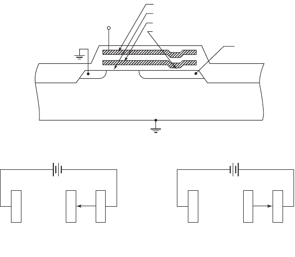
An example of a sense amplifier to detect the charge stored in the memory cell
is shown in Figure 16.82. On one side of the amplifier is a memory cell that either
stores a full charge or is empty, depending on the binary value of the data. On the
other side of the amplifier is a reference cell with a reference or dummy storage ca-
pacitor
C
R
that is one-half the value of the storage capacitor. The charge on
C
R
will
then be one-half the logic 1 charge on
C
S
. A cross-coupled dynamic latch circuit is
used to detect the small voltage differences and to restore the signal levels. The ca-
pacitors
C
D
and
C
DR
represent the relatively large parasitic bit line and reference bit
line capacitances.
In the standby mode, the bit lines on both sides of the sense amplifier are
precharged to the same potential. During the read cycle, both the WL and D–WL
nea80644_ch16_1145-1254.qxd 07/12/2009 3:38 Page 1220 pinnacle MHDQ-New:MHDQ134:MHDQ134-16:
Chapter 16 MOSFET Digital Circuits 1221
address signals go high allowing the charges in the cells to be redistributed along the
bit lines. After the charge equalization and since the charge in the dummy cell is half
the full charge, then
v
1
<v
2
when the memory cell is empty or a logic 0, and
v
1
>v
2
when the memory cell is full or a logic 1. The sense amplifier detects and amplifies
the voltage difference between the bit lines, and will latch at the logic level stored in
the basic memory cell.
Test Your Understanding
TYU 16.16 A six-transistor CMOS SRAM cell is biased at
V
DD
= 2.5V
. The
transistor parameters are
V
TN
=+0.4V
,
V
TP
=−0.4V
, and
(μ
n
/μ
p
) = 2.5
.
Determine the relative width-to-length ratios such that Equations (16.81)
through (16.84) are satisfied in terms of read/write requirements. (Ans.
[(W/L)
nA
/(W/L
n1
)] = 0.526
,
[(W/L)
p
/(W/L)
nB
)] = 0.862)
TYU 16.17 A one-transistor DRAM cell is composed of a 0.05 pF storage capacitor and
an NMOS transistor with a 0.5 V threshold voltage. A logic 1 is written into the cell
when both the data line and row-select line are raised to 3 V. Sensing circuitry permits
the stored charge to decay to 50 percent of its original value. Refresh occurs every 1.5 ms.
Determine the maximum allowed leakage current that can exist. (Ans.
I = 41.7
pA)
16.10 READ-ONLY MEMORY
Objective: • Analyze read-only memories (ROM)
We consider several examples of read-only memories in this section. The intent is
again to provide an introduction to this type of memory. In the case of EPROMs and
EEPROMs, the development effort has been directed toward the characteristics of the
basic memory cell.
Row
select
WL
CE
M
5
f
2
v
1
v
2
V
DD
C
D
C
DR
C
R
D
R
M
R
D–WL
C
S
D
Figure 16.82 Sense amplifier configuration for dynamic RAM cell
nea80644_ch16_1145-1254.qxd 07/12/2009 3:38 Page 1221 pinnacle MHDQ-New:MHDQ134:MHDQ134-16:
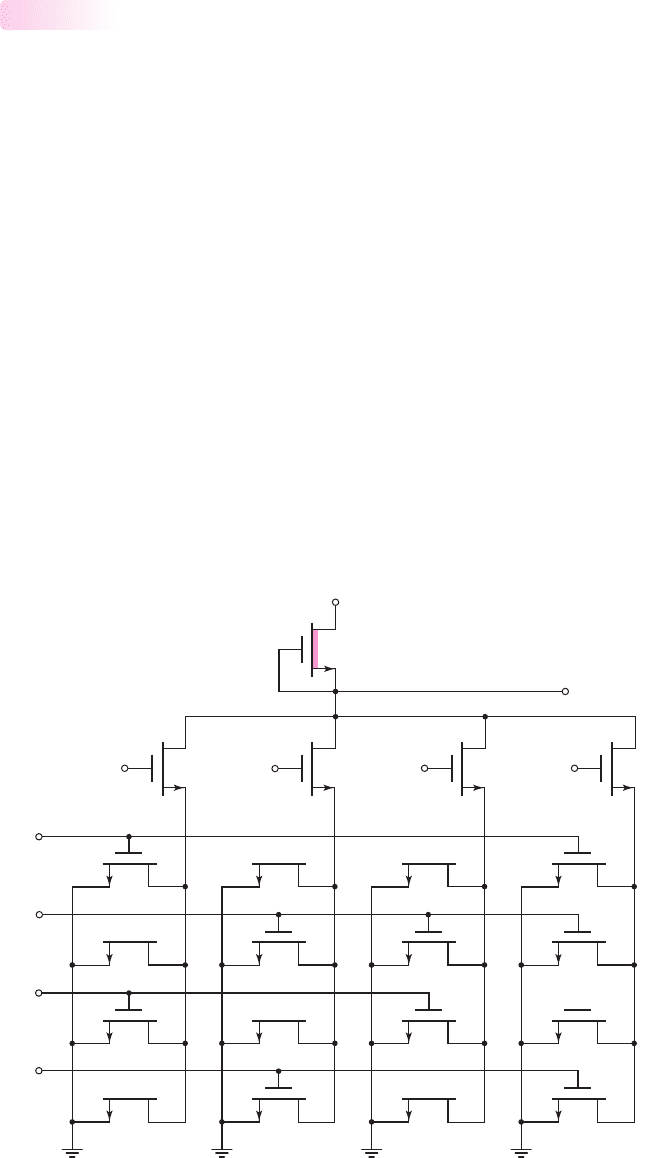
1222 Part 3 Digital Electronics
M
0
M
00
M
01
M
02
M
03
M
10
M
11
M
12
M
13
M
20
M
21
M
22
M
23
M
30
M
31
M
32
M
33
M
2
M
1
Y
0
Y
1
X
0
X
1
X
0
X
1
X
0
X
1
X
0
X
1
Y
0
Y
1
Y
0
Y
1
Y
0
Y
1
M
3
M
4
V
DD
v
O
–
–
––
–
–
––
Figure 16.83 An NMOS
16 ×1
mask-programmable ROM
ROM and PROM Cells
We consider two types of ROMs. The first example is a mask-programmed ROM, in
which contacts to devices are selectively included or excluded in the final manufac-
turing process to obtain the desired memory pattern. Figure 16.83 shows an example
of an NMOS
16 × 1
mask-programmed ROM. Enhancement-mode NMOS transis-
tors are fabricated in each of the 16 cell positions (the substrate connections are
omitted for clarity). However, gate connections are fabricated only on selected tran-
sistors. The transistors
M
1
–M
4
are column-select transistors and
M
0
is a depletion-
mode load device.
The inputs
X
O
,
X
1
,
Y
O
, and
Y
1
are the row- and column-select signals. If, for
example,
X
O
=
¯
X
1
=
¯
Y
O
= Y
1
= 1
, then the
M
12
transistor is addressed. Transis-
tors
M
12
and
M
3
turn on with this address, forcing the output to a logic 0. If the
address changes, for example, to
¯
X
O
= X
1
=
¯
Y
O
=
¯
Y
1
= 1
, then the transistor
M
23
is addressed. However, this transistor does not have a gate connection and consequently
never turns on, so the output is a logic 1.
The mask-programmed memory discussed is only a
16 × 1
-bit ROM, while a
more useful memory would contain many more bits. Memories can be organized in
any desired manner, such as a
2048 × 8
for a 16-K memory. This ROM is a non-
volatile memory, since the data stored are not lost when power is removed.
The second example of a ROM is a user-programmed ROM. The data pattern is
defined by the user after the final manufacture rather than during the manufacture.
16.10.1
nea80644_ch16_1145-1254.qxd 07/12/2009 3:38 Page 1222 pinnacle MHDQ-New:MHDQ134:MHDQ134-16:
Chapter 16 MOSFET Digital Circuits 1223
Q
00
Q
01
Q
02
Q
03
Q
10
Q
11
Q
12
Q
13
Q
20
Q
21
Q
22
Q
23
Q
30
Q
31
N
1
N
2
N
3
N
4
CS
Out
p
ut
Data line
Q
32
Q
33
X
0
X
1
V
CC
V
CC
V
CC
V
CC
–
X
0
X
1
–
X
0
X
1
––
Y
0
Y
1
Y
0
Y
1
–
Y
0
Y
1
–
Y
0
Y
1
––
X
0
X
1
(Row select)
Figure 16.84 A bipolar fuse-linked user-programmable ROM
One specific type is shown schematically in Figure 16.84. A small fuse is in series
with each emitter and can be selectively “blown” or left in place by the user. If, for
example, the fuse in
Q
00
is left in place and this transistor is addressed by
X
O
= X
1
= Y
O
= Y
1
= 1
, then
Q
00
turns on, raising the data line voltage at the
emitter of
Q
00
. The inverter
N
1
is enabled, making the output a logic 0. If the fuse is
blown in this transistor, then the input to the inverter is a logic 0, so the output is a
logic 1.
The polysilicon fuse in the emitter of an npn bipolar transistor has a fairly low
resistance, so with the fuse in place and at low currents, there is very little voltage
drop across the fuse. When the current through the fuse is increased to the 20 to
30 mA range, the heating of the polysilicon fuse causes the temperature to increase.
The silicon oxidizes, forming an insulator that effectively opens the path between the
data line and the emitter. The bipolar ROM circuit with the fuses either in place or
“blown” form a permanent ROM that is not alterable and is also nonvolatile.
nea80644_ch16_1145-1254.qxd 07/12/2009 3:38 Page 1223 pinnacle MHDQ-New:MHDQ134:MHDQ134-16:
1224 Part 3 Digital Electronics
Gate 2
Gate 2
Gate 1
Drain
Gate 1
C
1
C
2
S
B
D
Thin oxide
Source
Body
(a)
(b)
p
SiO
2
n
+
p
+
p
+
n
+
SiO
2
Figure 16.85 (a) Cross section of erasable programmable ROM; (b) equivalent circuit
EPROM and EEPROM Cells
An EPROM transistor is shown in Figure 16.85. The device has a double gate, with
gate 1 being a “floating gate” that has no electrical contact. Gate 2 is used for cell
selection, taking the role of the single gate of an MOS transistor.
Operation of this EPROM cell relies on being able to store charge on the float-
ing gate. Initially, we assume no charge on the floating gate so that with gate 2, drain,
and source grounded, the potential of gate 1 is also zero. As the voltage on gate 2 in-
creases, the gate 1 voltage rises also, but at a lower rate as determined by the capac-
itive divider. The net effect of this is to effectively raise the threshold voltage of this
MOSFET as seen from gate 2. However, when the gate 2 voltage is raised sufficiently
(approximately twice the normal threshold voltage), a channel forms. Under these
conditions, the device provides a stored logic 0 when used in the NOR array.
To write a logic 1 into this cell, both gate 2 and drain are raised to about 25 V
while the source and substrate remain at ground potential. A relatively large drain
current flows because of normal device conduction characteristics. In addition, the
high field in the drain–substrate depletion region results in avalanche breakdown of
the drain–substrate junction, with a considerable additional flow of current. The high
field in the drain depletion region accelerates electrons to high velocity such that a
small fraction traverse the thin oxide and become trapped on gate 1. When the gate 2
and drain potentials are reduced to zero, the negative charge on gate 1 forces its po-
tential to approximately
−5V
. If the gate 2 voltage for reading is limited to +5 V,
then a channel never forms. Thus a logic 1 is stored in the cell.
Gate 1 is completely surrounded by silicon dioxide (
SiO
2
), an excellent insula-
tor, so charge can be stored for many years. Data can be erased, however, by expos-
ing the cells to strong ultraviolet (UV) light. The UV radiation generates
electron–hole pairs in the
SiO
2
making the material slightly conductive. The negative
charge on the gate can then leak off, restoring the transistor to its original uncharged
condition. These EPROMs must be assembled in packages with transparent covers so
16.10.2
nea80644_ch16_1145-1254.qxd 07/12/2009 3:38 Page 1224 pinnacle MHDQ-New:MHDQ134:MHDQ134-16:
Chapter 16 MOSFET Digital Circuits 1225
Control gate
Gate oxide
Floating gate
Tunnel oxide
Field oxide
p substrate
(a)
(b) (c)
20 V –20 V
–
–
–
–
–
–
–
–
–
+
+– –+
+
+
+
+
+
+
+
–
–
–
–
–
–
–
–
–
Control
gate
Floating
gate
Drain Control
gate
Floating
gate
Drain
+V
G
n
+
n
+
+V
D
Figure 16.86 (a) Cross section of a floating-gate electrically erasable programmable ROM;
(b) charging the floating gate; (c) discharging the floating gate
the silicon chip may be exposed to UV radiation. One disadvantage is that the entire
memory must be erased before any reprogramming can be done. In general, repro-
gramming must also be done on specialized equipment; therefore, the EPROM must
be removed from the circuit during this operation.
In the EEPROM, each individual cell can be erased and reprogrammed without
disturbing any other cell. The most common form of EEPROM is also a floating gate
structure; one example is shown in Figure 16.86(a). The memory transistor is similar
to an n-channel MOSFET, but with a physical difference in the gate insulator region.
Charge may exist on the floating gate that will alter the threshold voltage of the de-
vice. If a net positive charge exists on the floating gate, the n-channel MOSFET is
turned on, whereas if zero or negative charge exists on the floating gate, the device is
turned off.
The floating gate is capacitively coupled to the control gate with the tunnel oxide
thickness less than 200 Å. If 20 V is applied to the control gate while keeping
V
D
= 0
,
electrons tunnel from the n
+
-drain region to the floating gate as demonstrated in
Figure 16.86(b). This puts the MOSFET in the enhancement mode with a threshold
voltage of approximately 10 V, so the device is effectively off. If zero volts is applied
to the control gate and 20 V is applied to the drain terminal, then electrons tunnel
from the floating gate to the n
+
-drain terminal as demonstrated in Figure 16.86(c).
This leaves a net positive charge on the floating gate that puts the device in the de-
pletion mode with a threshold voltage of approximately
−2V
, so the device is effec-
tively on. If all voltages are kept to within 5 V during the read cycle, this structure can
retain its charge for many years.
nea80644_ch16_1145-1254.qxd 07/12/2009 3:38 Page 1225 pinnacle MHDQ-New:MHDQ134:MHDQ134-16:

1226 Part 3 Digital Electronics
A/D
converter
D/A
converter
b
1
b
2
b
N
v
A
v
A
′
b
1
b
2
b
N
(a) (b)
…
…
Figure 16.87 Block diagram representations of (a) A/D converter and (b) D/A converter
16.11 DATA CONVERTERS
Objective: • Discuss the basic concepts in A/D and D/A converters.
Most physical signals exist in analog form. These signals include, for example, audio
or speech and the output of transducer circuits. Some analog signal processing, such
as amplifying the output of a microphone prior to the connection to speakers, may
occur. However, digital signal processing may be required to convert an analog sig-
nal into digital form prior to transmission of the signal to a satellite receiver, for ex-
ample. Therefore, analog-to-digital (A/D) and digital-to-analog (D/A) converters are
an important class of integrated circuits.
Basic A/D and D/A Concepts
In this section, we briefly consider a few basic concepts used in A/D and D/A con-
versions. Figure 16.87 shows the block diagram representations of A/D and D/A
converters. An analog signal
v
A
is applied to the input of the A/D converter and the
output is an N-bit digital signal that can be represented as
v
D
=
b
1
2
1
+
b
2
2
2
+
b
3
2
3
+···+
b
N
2
N
(16.85)
where
b
1
,
b
2
, etc. are the bit coefficients that are either a 1 or 0. The bit
b
1
is the most
significant bit (MSB) and the bit
b
N
is the least significant bit (LSB). The input to the
D/A converter is the N-bit digital signal and the output is an analog signal
v
A
. Ideally,
the output analog signal
v
A
is an exact replication of the input analog signal
v
A
.
16.11.1
The analog signal is to be converted to a digital form as indicated in Equa-
tion (16.85). Consider, for example, an analog signal represented by a voltage in the
range
0 ≤ v
A
≤ 5V
. Assume the digital signal is a 6-bit word. The 6-bit word repre-
sents 64 discrete values. The analog signal will then be divided into 64 values, with
each bit representing 5 V/64
=
0.078125 V. The analog-to-digital conversion can be
visualized in Figure 16.88.
When the analog input voltage is, for example,
v
A
=
5
64
V
, the digital output is
000001 and when the analog input voltage is
v
A
= 2(
5
64
) V
, the digital output is
000010. However, we see that when the input is in the range
1
2
(
5
64
)<v
A
<
3
2
(
5
64
) V
,
the digital output is constant at
v
D
= 000001
. There is an inherent quantization error
in the A/D conversion. A larger number of bits in the digital signal reduces the quan-
tization error, but requires a more complex circuit.
The same effect occurs at the output of the D/A converter. Since the digital input
signal exists in discrete steps or increments, the output signal will also occur in
discrete steps or increments. An example is shown in Figure 16.89. The output signal
nea80644_ch16_1145-1254.qxd 07/12/2009 3:38 Page 1226 pinnacle MHDQ-New:MHDQ134:MHDQ134-16:
Chapter 16 MOSFET Digital Circuits 1227
Analog
output
Time
v
A
″
v
A
′
Figure 16.89 Discrete analog output
v
A
and smoothed
output
v
A
versus time from a D/A converter
–
+
R
1
= 20 kΩ
V
R
= –5 V
R
F
v
O
S
1
S
2
S
3
S
4
R
2
= 40 kΩ
R
3
= 80 kΩ
R
4
= 160 kΩ
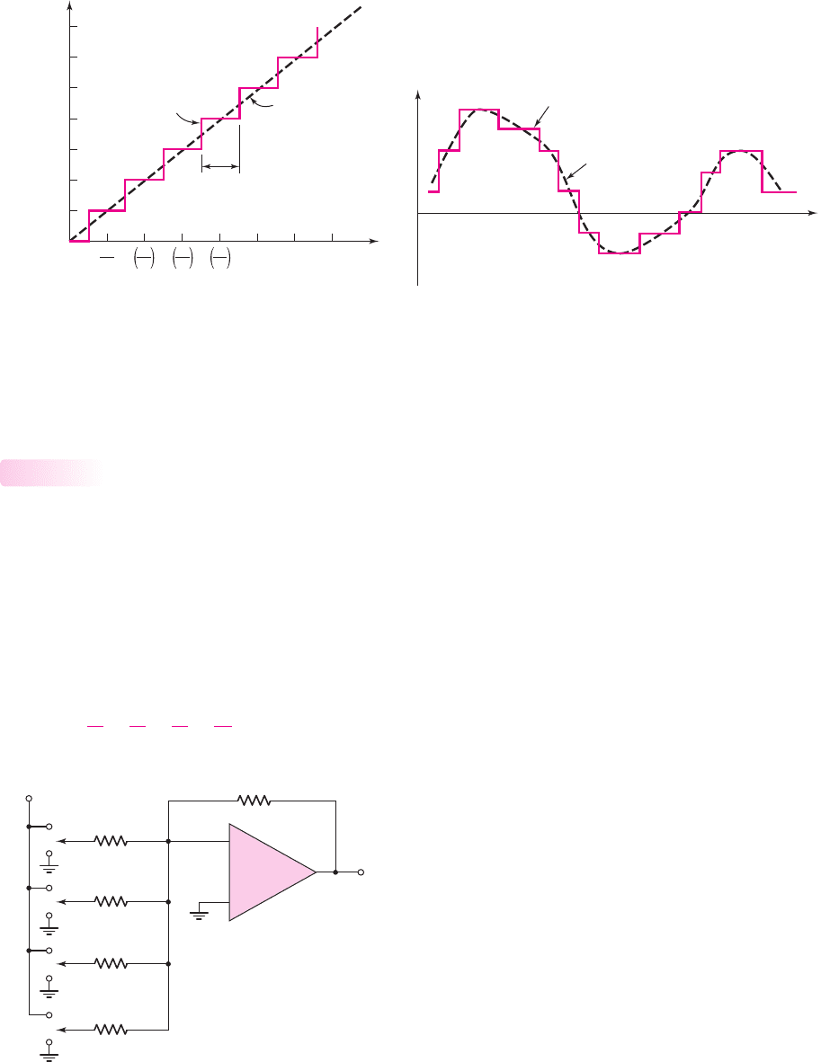
Figure 16.90 A 4-bit weighted-resistor D/A converter
v
A
is in the form of stair steps. Normally, this signal will be fed through a low-pass
filter to smooth out the signal to produce the dotted signal
v
A
in the figure. The de-
sired result is that the signal
v
A
be as close to the original signal
v
A
as possible.
Digital-to-Analog Converters
We will consider a few basic D/A converters to gain an appreciation of the techniques
used in these circuits.
Weighted-Resistor 4-Bit D/A
A simple circuit for a 4-bit D/A converter was shown in Chapter 9 in Figure P9.37.
This circuit is repeated here in Figure 16.90 for convenience. The circuit is a sum-
ming amplifier and includes a reference voltage
V
R
, four weighted input resistors,
four switches, and an op-amp with a feedback resistor. With
R
F
= 10 k
, we find
the output voltage to be
v
O
=
b
1
2
+
b
2
4
+
b
3
8
+
b
4
16
(5) V
(16.86)
16.11.2
000111
000110
000101
000100
000011
000010
1 LSB
Digital output voltage, v
D
Analog input voltage, v
A
000001
0
2
5
64
5
64
3
5
64
4
5
64
v
A
v
D
…
Figure 16.88 Digital output versus analog input for
a 6-bit A/D converter
nea80644_ch16_1145-1254.qxd 07/12/2009 3:38 Page 1227 pinnacle MHDQ-New:MHDQ134:MHDQ134-16: