Neamen D. Microelectronics: Circuit Analysis and Design
Подождите немного. Документ загружается.

1228 Part 3 Digital Electronics
+
–
Q
B1
V
Bias
R
V
REF
V
–
b
1
Q
R
R
F
v
o
I
R
–
+
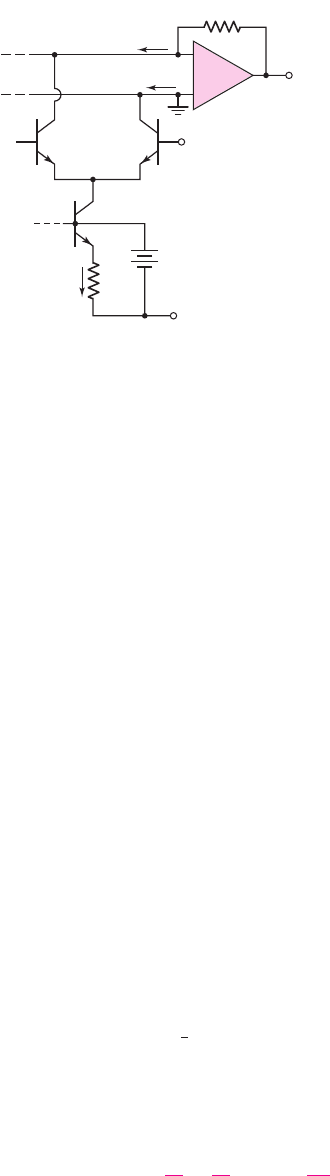
Figure 16.91 Example of a current switch in the MSB position in a weighted resistor of D/A
converter
One factor that determines the accuracy of the circuit is the precision of the
weighted input resistors and the feedback resistor. As the number of bits increases,
the size of the weighted input resistance increases for the lesser significant bits. The
accuracy for large resistance values becomes more difficult to maintain. The size of
this D/A converter is in general limited to a 4-bit input.
Another factor that determines the accuracy of the D/A circuit is the precision of the
switches. An example of a current switch, showing only the MSB, is shown in Figure
16.91. If the bit
b
1
is a logic 1 (
>V
Bias
), then
Q
B1
is turned on and
Q
R
is turned off so
that the current
I
R
is switched through
Q
B1
. This current becomes a component of the
current through the feedback resistor. If
b
1
is a logic 0 (
<V
Bias
), then
Q
B1
is turned off
and
Q
R
is turned on so that the current is switched to ground. Because of the virtual
ground, we may note that the collector voltages of
Q
B1
and
Q
R
are essentially identical.
For the circuit to operate properly, the base-emitter voltage of all the transistors
must be the same. Since the currents are smaller for the lesser significant bits, the
base–emitter areas must be reduced in order to maintain the same current density.
The type of circuit shown in Figure 16.91 then requires a wide range of base–emitter
areas in the same way that it requires a wide range of weighted resistor values.
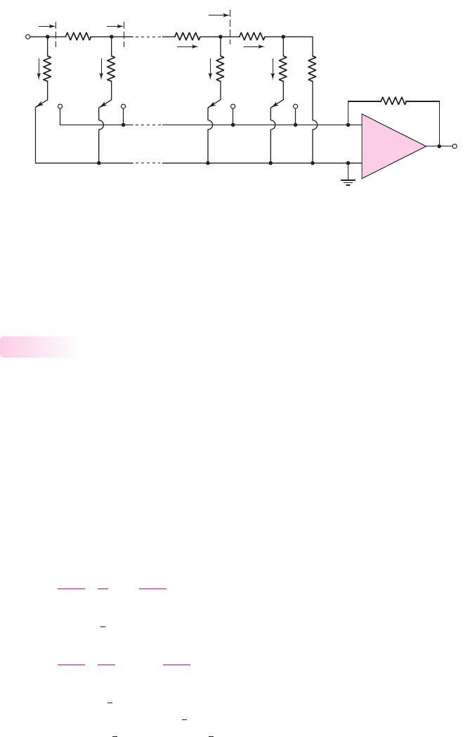
R–2R Ladder Network D/A
A circuit that eliminates the wide spread in weighted input resistor values in the
previous circuit is an R–2R ladder resistive network. Consider the circuit shown in
Figure 16.92. Assuming the switches are ideal, the current in each resistor is a
constant because of the virtual ground concept.
Consider node X in the circuit. We can note that the resistance denoted as
R
X
is
R
X
= 2R
. This same resistance occurs at every node in the circuit as indicated on the
figure. Therefore, the current entering each node splits evenly as shown at node X.
We have that
I
N−1
=
1
2
I
N−2
. This effect again occurs at every node in the circuit.
Therefore, we have
I
1
= 2I
2
= 4I
3
=···=2
N−2
I
N−1
= 2
N−1
I
N
(16.87)
Setting the feedback resistance to
R
F
= R
, we have the output voltage given by
v
O
=
(
−V
REF
)
b
1
2
+
b
2
4
+···+
b
N
2
N
(16.88)
nea80644_ch16_1145-1254.qxd 07/12/2009 3:38 Page 1228 pinnacle MHDQ-New:MHDQ134:MHDQ134-16:
Chapter 16 MOSFET Digital Circuits 1229
The circuit in Figure 16.92 requires only two resistance values. These resistance
values can then be held to tight tolerances.
There are a variety of D/A converter designs that will not be pursued in this text.
This short discussion provides a brief introduction to D/A design.
Analog-to-Digital Converters
As in the previous section, we will consider a few basic A/D converters to gain an ap-
preciation of the techniques used in these circuits.
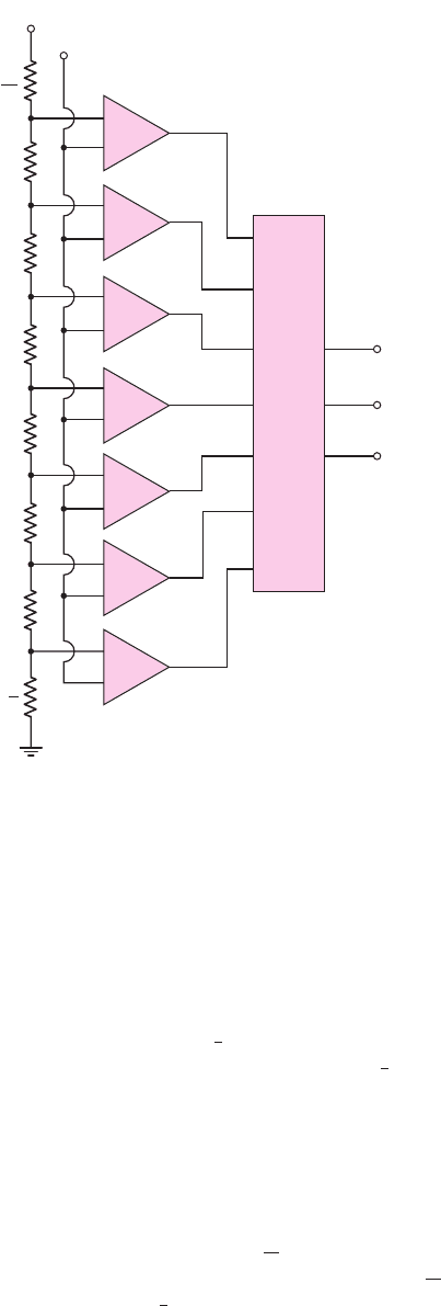
Parallel or Flash A/D
The fastest A/D converter, and perhaps simplest in concept, is the parallel A/D or
flash converter. Figure 16.93 shows a 3-bit flash A/D converter. The analog input sig-
nal
v
A
is applied to seven comparators at the noninverting terminals. A reference
voltage is applied to a resistive ladder network. The outputs of the ladder network are
applied to the inverting terminals of the comparators.
The total resistance in the ladder network is 8R so
V
REF
/8R
represents 1 LSB in
terms of current. The smallest output voltage is
v
1
=
V
REF
8R
R
2
=
V
REF
16
(16.89)
which represents
1
2
LSB. The second output voltage is
v
2
=
V
REF
8R
3R
2
= 3
V
REF
16
(16.90)
which represents
1
1
2
LSB.
If the analog input is
v
A
<
1
2
LSB, the output of all comparators will be low. If
the analog input is
1
2
LSB <v
A
< 1
1
2
LSB
, the output of the first comparator goes
high. As the analog input voltage increases, the outputs of additional comparators
go high. The combinational logic network then produces the desired 3-bit output
word. We can note that a complete conversion is obtained during one clock period.
A disadvantage of the flash A/D converter is that the number of resistors and
comparators increases rapidly as the desired number of output bits increases. We
see that
2
N
resistors and
2
N
−1
comparators are required. Thus, for a 10 bit word,
16.11.3
V
REF
R
X
= 2R
R
F
2R2R2R2R2R
2R 2R
RRR
X
v
O
I
1
b
1
b
2
b
N–1
b
N
I
2
I
N–1
I
N–2
I
N–1
I
N
–
+
Figure 16.92 Example of an R–2R ladder network in an N-bit D/A converter
nea80644_ch16_1145-1254.qxd 07/12/2009 3:38 Page 1229 pinnacle MHDQ-New:MHDQ134:MHDQ134-16:
1230 Part 3 Digital Electronics
–
+
–
+
–
+
–
+
–
+
–
+
–
+
Combinational logic
R
R
R
R
R
R
v
A
R
2
3R
2
V
REF
b
1
b
2
b
3
v
1
v
2
Figure 16.93 A 3-bit flash or parallel A/D converter
1024 resistors and 1023 comparators are required. However, 10-bit resolution A/D
flash converters have been fabricated as ICs.
Counting A/D
A second type of A/D converter is the counting converter. This system contains a
comparator, a counter, and a D/A converter in a feedback configuration as shown in
Figure 16.94(a). Additional control circuitry is not shown for simplicity.
Initially the output of the counter is set equal to zero and the output of the D/A
converter is set to
v
O
=
1
2
LSB
. When an analog input voltage
v
A
is applied, the out-
put of the comparator is high (unless
v
A
<
1
2
LSB), which enables the counter. Then
for each clock pulse, the output of the counter increases by one, producing an N-bit
digital output. When the output of the D/A becomes just greater than the analog
input voltage, the output of the comparator goes low and the counter is disabled. The
N-bit digital output then corresponds to the analog input signal.
Figure 16.94(b) shows the timing diagram of a counting converter for a 4-bit
digital output. Assume that the analog input signal is in the range
0 ≤ v
A
≤ 5V
.
A 1 LSB then corresponds to
5
16
V.
Assume the analog input signal is
v
A
= 5.2(
5
16
) V
. The initial output of the D/A,
as mentioned, is a
1
2
LSB offset voltage. By including the offset voltage, the maximum
nea80644_ch16_1145-1254.qxd 07/12/2009 3:38 Page 1230 pinnacle MHDQ-New:MHDQ134:MHDQ134-16:
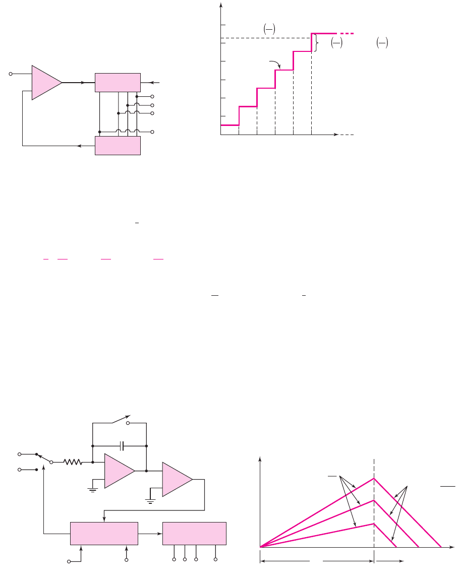
Chapter 16 MOSFET Digital Circuits 1231
quantization error will then be
±
1
2
LSB. We see from Figure 16.94(b) that after the
fifth clock pulse, the output of the D/A is
v
O
=
1
2
5
16
+5
5
16
= 5.5
5
16
V
(16.91)
which is larger than
v
A
. The counter then stops counting and the digital output is 0101.
We can note that the digital output corresponds to
5(
5
16
)
V, which is within
1
2
LSB of
the analog input signal.
To complete the conversion process, the clock must go through its complete
cycle, which for a 4-bit output is 16 clock periods.
Dual-Slope A/D
Another type of A/D conversion scheme is the dual-slope A/D converter shown in
Figure 16.95(a). This type of converter is found in high-resolution data acquisition
systems, for example, since 20-bit conversions can be achieved.
+
–
0110
N-bit
output
Comparator
0101
0100
0011
0010
0001
0000
0123
Clock pulses
45
4.5 < v
A
< 5.5
5
16
5
16
5
16
v
A
= 5.2 V
v
O
v
O
v
A
Counter Clock
…
…
…
D/A
converter
b
1
b
2
b
3
b
N
(a)
(b)
V
Figure 16.94 (a) Block diagram of a counting A/D converter and (b) the timing diagram of a
4-bit A/D counting converter for a specific input voltage
–
+
–
+
Control
logic
Set/reset
Clock
…
Time
Counter
Integrator
Comparator
C
R
S
1
v
O1
S
2
b
1
T
1
T
2
b
2
b
3
b
N
V
REF
–v
A
′
v
O1
Slope =
RC
v
A
′
Slope = –
RC
V
REF
(a) (b)
Figure 16.95 (a) Block diagram and (b) timing diagram of a dual-slope A/D converter
nea80644_ch16_1145-1254.qxd 07/12/2009 3:38 Page 1231 pinnacle MHDQ-New:MHDQ134:MHDQ134-16:

1232 Part 3 Digital Electronics
From Figure 16.95(a), at
t = 0
, the reset switch
S
1
opens and a negative input
signal
(−v
A
)
is applied to the integrator. The input signal
v
A
is a sampled portion of
the analog signal
v
A
and hence is a constant during the conversion process. The out-
put
v
O1
of the integrator is a positive linear signal as shown in the timing diagram in
Figure 16.95(b). The slope of the signal is proportional to the value of
v
A
. This por-
tion of the conversion process continues for a fixed time
T
1
, at which time the counter
has reached its maximum value and overflows.
At this time, the input switch
S
2
changes to a positive input reference voltage
V
REF
. The output of the integrator starts at the peak output voltage reached at
T
1
and
now has a negative slope. The counter has been reset and is now counting. The count-
ing stops when the output voltage
v
O1
reaches zero.
The time
T
2
is related to
T
1
and
v
A
by
T
2
= T
1
v
A
V
REF
(16.92)
The counter reading at
T
2
is given by
n = 2
N
v
A
V
REF
(16.93)
The output of the counter is then the digital equivalent of
v
A
.
The output of the dual-slope A/D converter is independent of the actual values of
R and C and hence is very accurate. The disadvantage of this data converter is that it
is a fairly slow system. The time
T
1
requires
2
N
clock pulses and the maximum pos-
sible time
T
2
would also require
2
N
clock pulses. For example, a 12-bit A/D con-
verter would require a total of 8192 clock pulses. This corresponds to a conversion
time of 8.2 ms for a 1 MHz clock.
16.12 DESIGN APPLICATION: A STATIC CMOS
LOGIC GATE
Objective: • Design a static CMOS logic gate to implement a specific
logic function.
Specifications: A static CMOS logic gate is to be designed that implements the
function of a three-input odd-parity checker. The output is to be high when an odd
number of inputs are high. The size of each transistor is to be determined so that the
switching speed is the same as that of a basic CMOS inverter with
W
n
= W
and
W
p
= 2W
. A minimum number of transistors are to be used in the NMOS pull-down
and PMOS pull-up portions of the circuit.
Choices: We will assume that input signals A, B, and C as well as the complements
¯
A
,
¯
B
, and
¯
C
are available.
Solution (Logic Function): The output of the logic gate is to be high when one
input is high or when all three inputs are high. The output is to be high, for exam-
ple, when the inputs are
A = 1
and
B = C = 0
. The output would be high, then,
for
A
¯
B
¯
C = 1
. Considering the other possibilities, the logic function can be
written as
F = A
¯
B
¯
C +
¯
AB
¯
C +
¯
A
¯
BC + ABC
(16.94)
nea80644_ch16_1145-1254.qxd 07/12/2009 3:38 Page 1232 pinnacle MHDQ-New:MHDQ134:MHDQ134-16:
Chapter 16 MOSFET Digital Circuits 1233
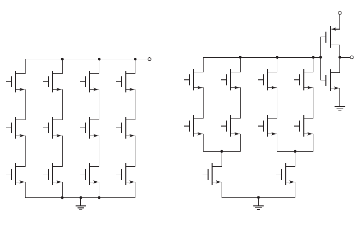
AAA
–
A
–
BBB
–
B
–
CC
V
+
C
––
C
C
–
C
F
–
AAA
–
A
–
BBB
–
B
–
F
–
F
(a) (b)
Figure 16.96 (a) The basic NMOS pull-down portion of the logic gate derived from the
logic function; (b) the modified NMOS pull-down portion of the logic gate for the design
application
Solution (NMOS Pull-Down): Figure 16.96(a) shows the basic NMOS pull-down
portion of the logic gate derived from the logic function given in Equation (16.94).
However, we may note that the two transistors at the bottom of the first two columns
have a common input of
¯
C
and the two transistors at the bottom of the last two
columns have a common input of C. The two transistors with common inputs can be
combined into a single transistor. The final design of the NMOS pull-down portion
of the logic gate is shown in Figure 16.96(b).
In order for the NMOS portion of the circuit to be in the pull-down mode, three
NMOS devices in series must be turned on. In order for this circuit to be equivalent
to the NMOS in the CMOS inverter, each NMOS device must have a width of
W
n
= 3W
.
Solution (PMOS Pull-Up): Figure 16.97(a) shows the basic PMOS pull-up
portion of the logic gate. This circuit is the complement of the NMOS circuit
shown in Figure 16.96(a). We may note that two transistors on the right side of the
circuit have common inputs C and
¯
C
. Each pair of transistors is effectively in
series and hence can be replaced by a single transistor. The resulting circuit is
shown in Figure 16.97(b). The complete three-input odd-parity checker circuit
is then the combination of Figures 16.96(b) and 16.97(b) along with a CMOS
inverter on the output.
Comment: The basic logic circuit can be derived from the logic function.
However, as we have seen, some simplifications can be made in the design. These
simplifications can also be obtained from simplifications in the basic logic
function also.
nea80644_ch16_1145-1254.qxd 07/12/2009 3:38 Page 1233 pinnacle MHDQ-New:MHDQ134:MHDQ134-16:

1234 Part 3 Digital Electronics
ABC
V
+
F
–
(a) (b)
B
–
A
–
C
BA
–
C
–
AB
–
C
–
C
–
C
AB
V
+
F
–
B
–
A
–
BA
–
AB
–
Figure 16.97 (a) The basic PMOS pull-up portion of the logic gate derived as the
complement of the basic NMOS pull-down circuit; (b) the modified PMOS pull-up portion
of the logic gate for the design application
16.13 SUMMARY
• In this chapter, NMOS and CMOS digital logic circuits were analyzed and
designed. These circuits include basic logic gates, shift registers, flip-flops, and
memories.
• The NMOS inverter is the basis of NMOS logic circuits. The quasi-static voltage
transfer characteristics of NMOS inverters with resistive-load, enhancement-
load, and depletion-load devices were generated.
• The basic NMOS NOR and NAND logic gates were analyzed. More sophisti-
cated logic functions can be implemented by combining driver transistors in par-
allel and series combinations.
• The CMOS inverter is the basis of CMOS logic circuits. The quasi-static voltage
transfer characteristics were generated. For the CMOS circuit, the quiescent
power dissipation is essentially zero when the input is in either logic state.
• The basic CMOS NOR and NAND logic gates were analyzed. More sophisti-
cated CMOS logic circuits were also analyzed and designed. Transistor width-to-
length ratios were designed to provide equal current drive in the NMOS pull-
down and PMOS pull-up portions of the circuit.
• CMOS clocked logic circuits can be designed to reduce the number of required
PMOS devices. A generalized NMOS logic circuit is inserted between clocked
PMOS and NMOS devices. The advantage of low static power dissipation is
maintained.
• Sequential logic circuits, such as shift registers, flip-flops, and a full one-bit
adder, were analyzed.
nea80644_ch16_1145-1254.qxd 07/12/2009 3:38 Page 1234 pinnacle MHDQ-New:MHDQ134:MHDQ134-16:

Chapter 16 MOSFET Digital Circuits 1235
• A whole classification of circuits called memories was considered. In the
NMOS SRAM, static power is continuously dissipated in the cell, which lim-
its the size of the memory because of the total chip power limitation. The pri-
mary advantage of a CMOS SRAM is that there is essentially no static power
dissipation. The size of a CMOS memory is limited primarily by chip area
requirements.
• Read-only-memory (ROM and PROM) contains fixed data that are implemented
by the manufacturer or by the user. In both cases, the data cannot be altered.
EPROM and EEPROM cells contain MOSFETs with floating gates that can be
either charged or left uncharged by the user depending on whether logic 1 or a
logic 0 is to be stored.
• The basic concepts used in A/D and D/A converters were discussed. A few
examples of D/A converter circuits and A/D converter systems were analyzed.
• As an application, a static CMOS logic circuit to implement a specific logic func-
tion is designed.
CHECKPOINT
After studying this chapter, the reader should have the ability to:
✓ Analyze the transfer characteristics of NMOS inverters, including the determi-
nation of noise margins.
✓ Design an NMOS logic circuit to perform a specific logic function.
✓ Analyze the transfer characteristics of the CMOS inverter, including the deter-
mination of switching power and noise margins.
✓ Design a CMOS logic circuit to perform a specific logic function.
✓ Design a clocked CMOS logic circuit to perform a specific logic function.
✓ Design an NMOS or CMOS pass network to perform a specific logic function.
✓ Design an NMOS or CMOS RAM cell and design a simple sense amplifier.
✓ Analyze the R–2R ladder network used in a D/A converter circuit.
✓ Describe the characteristics of a 3-bit flash A/D converter and describe the oper-
ation of the dual-slope A/D converter.
REVIEW QUESTIONS
1. Sketch the quasi-static voltage transfer characteristics of an NMOS inverter with
depletion load. What effect does changing the transistor
W/L
ratio have on the
transfer characteristics?
2. Sketch an NMOS three-input NOR logic gate. Describe its operation. Discuss
the condition under which the maximum logic 0 value is obtained.
3. Discuss how more sophisticated (compared to the basic NOR and NAND) logic
functions can be implemented in a single NMOS logic circuit.
4. Sketch the quasi-static voltage transfer characteristics of a CMOS inverter. Dis-
cuss the various intervals in terms of transistor bias. What is the effect on the
transfer curve of changing the transistor
W/L
ratios? What is the advantage of
the CMOS inverter compared to an NMOS inverter?
5. Discuss the parameters that affect the switching power dissipation in a CMOS
inverter.
nea80644_ch16_1145-1254.qxd 07/12/2009 3:38 Page 1235 pinnacle MHDQ-New:MHDQ134:MHDQ134-16:

1236 Part 3 Digital Electronics
6. Define the noise margin in a CMOS inverter.
7. Sketch a CMOS three-input NAND logic gate. Describe its operation. Deter-
mine the relative transistor
W/L
ratios to obtain equal pull-up and pull-down
switching times.
8. Discuss how more sophisticated (compared to the basic NOR and NAND) logic
functions can be implemented in a single CMOS logic circuit.
9. Discuss the basic principles of a clocked CMOS logic circuit.
10. Sketch an NMOS transmission gate and describe its operation. What is the max-
imum output voltage?
11. Sketch a CMOS transmission gate and describe its operation. Why is the quasi-
static output voltage always equal to the quasi-static input voltage?
12. Discuss what is meant by pass transistor logic.
13. If an NMOS or CMOS transmission gate is turned off (an open switch), discuss
why the output voltage is, in general, not stable.
14. Sketch an NMOS dynamic shift register and describe its operation.
15. Sketch a CMOS R–S flip flop and describe its operation. Why must the input
condition
R = S = 1
be avoided?
16. Describe the basic architecture of a semiconductor random-access memory.
17. Sketch a CMOS SRAM cell and describe its operation. Discuss any advantages
and disadvantages of this design. Describe how the cell is addressed.
18. Sketch a one-transistor DRAM cell and describe its operation. What makes this
circuit dynamic?
19. Describe a mask-programmed MOSFET ROM memory.
20. Describe the basic operation of a floating gate MOSFET and how this can be
used in an erasable ROM.
PROBLEMS
[Note: In the following problems, unless otherwise stated, assume transistor para-
meters of
V
TNO
= 0.5
V,
V
TPO
=−0.5
V,
k
n
= 100 μ
A/V
2
, and
k
p
= 40 μ
A/V
2
.
Neglect the body effect unless otherwise stated and assume
T = 300
K.]
Section 16.1 NMOS Inverters
16.1 The load resistor in the NMOS inverter in Figure 16.3(a) is
R
D
= 40
k
. The
circuit is biased at
V
DD
= 3.3
V. (a) Design the transistor width-to-length
ratio such that
v
O
= 0.1
V when
v
I
= 3.3
V. (b) Using the results of part (a),
determine the transition point for the transistor. (c) Using the results of part
(a), find the maximum current and maximum power dissipation in the
inverter.
16.2 The inverter circuit in Figure 16.3(a) is biased at
V
DD
= 3.3
V. Assume
the transistor conduction parameter is
K
n
= 50 μ
A/V
2
. (a) Let
R
D
= 100
k
. (i) Determine the transition point. (ii) Determine
v
O
for
v
I
= 3.3
V. (b) Repeat part (a) for
R
D
= 30
k
. (c) Repeat part (a) for
R
D
= 5
k
.
D16.3 (a) Redesign the resistive load inverter in Figure 16.3(a) so that the
maximum power dissipation is 0.25 mW with
V
DD
= 3.3V
and
nea80644_ch16_1145-1254.qxd 07/15/2009 09:32 PM Page 1236 F506 Hard disk:Desktop Folder:ALI-07-15-09:

Chapter 16 MOSFET Digital Circuits 1237
v
O
= 0.15 V
when the input is a logic 1. (b) Using the results of part (a),
what is the input voltage range when the transistor is biased in the satura-
tion region?
D16.4 (a) Design the saturated load inverter circuit in Figure 16.5(a) such that the
power dissipation is 0.30 mW and the output voltage is 0.08 V for
v
I
= 1.4
V. The circuit is biased at
V
DD
= 1.8
V and the transistor thresh-
old voltage of each transistor is
V
TNO
= 0.4
V. (b) Using the results of part
(a), find the range of input voltage such that the driver transistor is biased in
the saturation region.
16.5 An NMOS inverter with saturated load is shown in Figure 16.5(a). The bias
is
V
DD
= 3V
and the transistor threshold voltages are 0.5 V. (a) Find the
ratio
K
D
/K
L
such that
v
O
= 0.25 V
when
v
I
= 3V
. (b) Repeat part (a) for
v
I
= 2.5V
. (c) If
W/L = 1
for the load transistor, determine the power
dissipation in the inverter for parts (a) and (b).
D16.6 Consider the NMOS inverter with saturated load in Figure 16.5(a). Let
V
DD
= 3
V. (a) Design the circuit such that the power dissipation in the
circuit is
400 μ
W and the output voltage is 0.10 V when the input voltage is
a logic 1. (b) Determine the transition point of the driver transistor.
16.7 The NMOS inverter with saturated load in Figure 16.5(a) operates with
a supply voltage of
V
DD
. The MOSFETs have threshold voltages of
V
TN
= 0.2 V
DD
. Determine
(W/L)
D
/(W/L)
L
such that
V
O
= 0.08 V
DD
.
Neglect the body effect.
16.8 The enhancement-load transistor in the NMOS inverter in Figure P16.8 has
a separate bias applied to the gate. Assume transistor parameters of
K
n
= 1 mA/V
2
for
M
D
,
K
n
= 0.4 mA/V
2
for
M
L
, and
V
TN
= 1V
for both
transistors. Using the appropriate logic 0 and logic 1 input voltages,
determine
V
OH
and
V
OL
for: (a)
V
B
= 4V
,(b)
V
B
= 5V
, (c)
V
B
= 6V
,
and (d)
V
B
= 7V
.
16.9 For the depletion load inverter shown in Figure 16.7(a), assume parameters
of
V
DD
= 3.3
V,
V
TND
= 0.5
V,
V
TNL
=−0.8
V,
K
D
= 500 μ
A/V
2
, and
K
L
= 100 μ
A/V
2
. (a) Find the transition points of the driver and load
transistors. (b) Determine
v
O
for
v
I
= 3.3
V. (c) Determine the maximum
current and maximum power dissipation in the circuit.
16.10 In the depletion-load NMOS inverter circuit in Figure 16.7(a), let
V
TND
= 0.5V
and
V
DD
= 3V
,
K
L
= 50 μA/V
2
, and
K
D
= 500 μA/V
2
.
Calculate the value of
V
TNL
such that
v
O
= 0.10 V
when
v
I
= 3V
.
D16.11 Consider the NMOS inverter with depletion load in Figure 16.7(a). Let
V
DD
= 1.8
V, and assume
V
TND
= 0.3
V and
V
TNL
=−0.6
V. (a) Design
the circuit such that the power dissipation is
80 μ
W and the output voltage is
v
O
= 0.06
V when
v
I
is a logic 1. (b) Using the results of part (a), determine
the transition points for the driver and load transistors. (c) If
(W/L)
D
found
in part (a) is doubled, what is the maximum power dissipation in the inverter
and what is
v
O
when
v
I
is a logic 1?
D16.12 The NMOS inverter with depletion load is shown in Figure 16.7(a).
The bias is
V
DD
= 2.5V
. The transistor parameters are
V
TND
= 0.5V
and
V
TNL
=−1
V. The width-to-length ratio of the load device is
W/L = 1
. (a) Design the driver transistor such that
v
O
= 0.05 V
when the
input is a logic 1. (b) What is the power dissipated in the circuit when
v
I
= 2.5V
?
M
D
M
L
V
B
v
O
v
I
V
DD
= 5 V
Figure P16.8
nea80644_ch16_1145-1254.qxd 07/12/2009 3:38 Page 1237 pinnacle MHDQ-New:MHDQ134:MHDQ134-16: