Neamen D. Microelectronics: Circuit Analysis and Design
Подождите немного. Документ загружается.


1238 Part 3 Digital Electronics
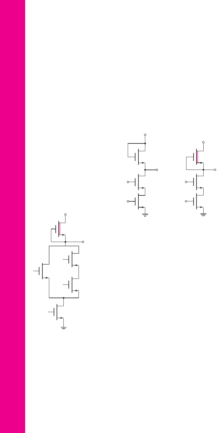
16.13 Calculate the power dissipated in each inverter circuit in Figure P16.13 for
the following input conditions: (a) Inverter a: (i)
v
I
= 0.5V
, (ii)
v
I
= 5V
;
(b) Inverter b: (i)
v
I
= 0.25 V
, (ii)
v
I
= 4.3V
; (c) Inverter c:
(i)
v
I
= 0.03 V
, (ii)
v
I
= 5V
.
V
DD
= 5 V
R
D
= 20 kΩ
v
O
v
I
V
TN
= 1.5 V
K
D
= 100 mA/V
2
v
O
v
I
V
DD
= 5 V
V
TNL
= 0.7 V
K
L
= 10 mA/V
2
V
TND
= 0.7 V
K
D
= 100 mA/V
2
I
D
v
I
v
O
V
DD
= 5 V
V
TND
= 1 V
K
D
= 100 mA/V
2
V
TNL
= –2 V
K
L
= 10 mA/V
2
(a) (b) (c)
Figure P16.13
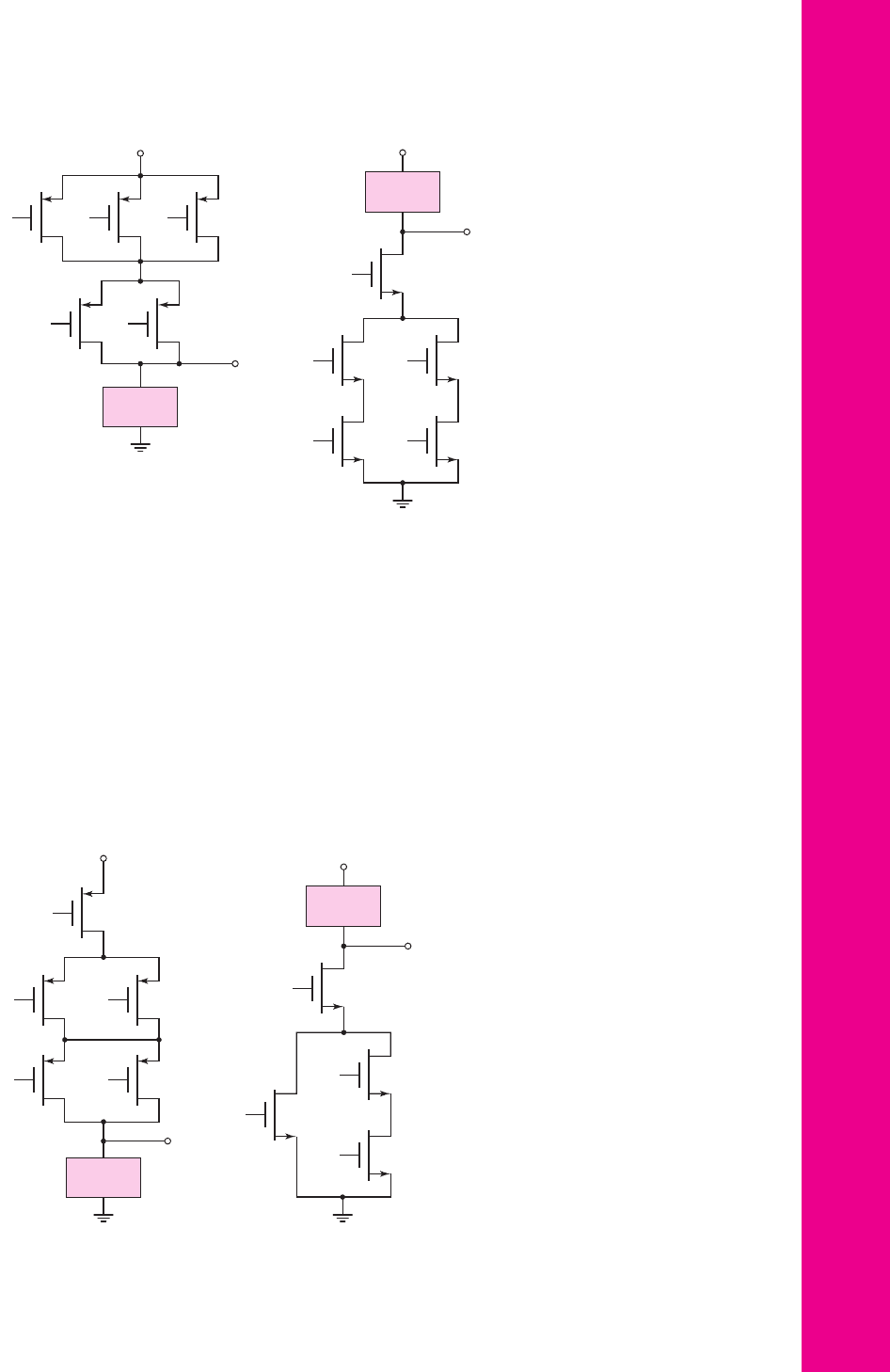
v
O2
v
O1
v
I
V
DD
= 5 V
M
D1
M
D2
M
L2
M
L1
Figure P16.14
v
O2
v
O1
v
I
V
DD
= 5 V
M
D1
M
D2
M
L2
M
L1
Figure P16.15
16.15 Consider the circuit in Figure P16.15. The parameters of the driver transis-
tors are
V
TND
= 0.8
V and
(W/L)
D
= 4
, and those of the load transistors
are
V
TNL
=−1.2
V and
(W/L)
L
= 1
. (a) If
v
I
is a logic 1, determine the
values of
v
O1
and
v
O2
. (b) Repeat part (a) if
v
I
is a logic 0.
16.16 For the saturated load inverter shown in Figure 16.9(a), assume transistor
parameters of
V
TNDO
= V
TNLO
= 0.5
V,
K
D
= 200 μA/V
2
,
K
L
=
20 μ
A/V
2
,
γ = 0.25
V
1/2
, and
φ
fp
= 0.35
V. Determine
v
O
for
v
I
= 0.12
V for the case when (a) the body effect is neglected and (b) the
body effect is taken into account.
16.17 Consider the NMOS inverter with depletion load in Figure 16.9(b). The
transistor parameters are
V
TNDO
= 0.4
V,
V
TNLO
=−0.6
V,
K
D
=
100 μ
A/V
2
,
K
L
= 20 μ
A/V
2
,
γ = 0.25
V
1/2
, and
φ
fp
= 0.35
V. Determine
v
I
when
v
O
= 1.25
V for the case when (a) the body effect is neglected and
(b) the body effect is taken into account.
16.14 For the two inverters in Figure P16.14, assume
(W/L)
L
= 1
for the load
devices and
(W/L)
D
= 10
for the driver devices. (a) If
v
I
is a logic 1,
determine the values of
v
O1
and
v
O2
. (b) Repeat part (a) if
v
I
is a logic 0.
nea80644_ch16_1145-1254.qxd 07/12/2009 3:38 Page 1238 pinnacle MHDQ-New:MHDQ134:MHDQ134-16:

Chapter 16 MOSFET Digital Circuits 1239
Section 16.2 NMOS Logic Circuits
16.18 Consider the circuit with a depletion load device shown in Figure P16.18.
(a) For
v
X
= 1.8
V and
v
Y
= 0.1
V, determine
K
D
/K
L
such that
v
O
= 0.1
V. (b) Using the results of part (a), determine
v
O
when
v
X
= v
Y
= 1.8
V. (c) If the width-to-length ratio of the depletion load is
(W/L)
L
= 1
, determine the power dissipation in the logic circuit for the
input conditions listed in parts (a) and (b).
5 V
5 V
M
D4
M
D2
v
X
v
O2
v
O3
v
O1
v
Y
M
D3
M
L3
5 V
M
D1
M
L2
M
L1
Figure P16.21
v
O
V
DD
= 1.8 V
M
X
v
X
v
Y
V
TND
= 0.4 V
M
Y
K
D
V
TNL
= –0.6 V
K
L
Figure P16.18
v
O
3 V
M
Y
v
Y
M
X
v
X
v
Z
V
TND
= +0.5 V
M
Z
K
D
V
TNL
= –1 V
K
L
Figure P16.19
D16.19 Consider the three-input NOR logic gate in Figure P16.19. The transistor
parameters are
V
TNL
=−1
V and
V
TND
= 0.5V
. The maximum value of
v
O
in its low state is to be 0.1 V. (a) Determine
K
D
/K
L
. (b) The maximum
power dissipation in the NOR logic gate is to be 0.1 mW. Determine the
width-to-length ratios of the transistors. (c) Determine
v
O
when
v
X
=v
Y
=
v
Z
= 3V
.
16.20 Consider a four-input NMOS NOR logic gate with a depletion load similar
to the circuit in Figure P16.19. Assume
V
DD
= 2.5
V,
V
TND
= 0.4
V, and
V
TNL
=−0.6
V. The maximum value of
v
O
in its low state is to be 50 mV.
(a) Determine
K
D
/K
L
. (b) The maximum power dissipation in this NOR
logic gate is to be
50 μ
W. Determine the width-to-length ratio of each tran-
sistor. (c) Determine
v
O
when (i) two inputs are a logic 1, (ii) three inputs
are a logic 1, and (iii) all inputs are a logic 1.
16.21 The transistor parameters for the circuit in Figure P16.21 are:
V
TN
=
0.8 V
for all enhancement-mode devices,
V
TN
=−2
V for the depletion-mode
nea80644_ch16_1145-1254.qxd 07/12/2009 3:38 Page 1239 pinnacle MHDQ-New:MHDQ134:MHDQ134-16:
1240 Part 3 Digital Electronics
devices, and
k
n
= 60 μA/V
2
for all devices. The width-to-length ratios of
M
L2
and
M
L3
are 1, and those for
M
D2
, M
D3
, and
M
D4
are 8. (a) For
v
X
= 5V
, output
v
O1
is 0.15 V, and the power dissipation in this inverter is
to be no more than 250
μ
W. Determine
(W/L)
ML1
and
(W/L)
MD1
. (b) For
v
X
= v
Y
= 0
, determine
v
O2
.
16.22 Consider the NMOS circuit in Figure P16.22. The transistor parameters
are
(W/L)
X
= (W/L)
Y
= 12
,
(W/L)
L
= 1
, and
V
TN
= 0.4
V. Neglect
the body effect. (a) Determine
v
O
when
v
X
= v
Y
= 2.9
V. (b) What are
the values of
v
GSX
,
v
GSY
,
v
DSX
, and
v
DSY
? [Hint: Set the drain current in
each device equal to each other. Also, neglect the terms
v
2
O
,
v
2
DSX
, and
v
2
DSY
].
V
DD
Y
A
D
B
C
Figure P16.25
v
O
v
Y
V
DD
= 5 V
v
X
M
X
M
Y
M
L
Figure P16.23
v
O
v
Y
V
DD
= 3.3 V
v
X
M
X
M
Y
M
L
Figure P16.22
16.23 In the NMOS circuit in Figure P16.23, the transistor parameters are:
(W/L)
X
=(W/L)
Y
=4
,
(W/L)
L
=1
,
V
TNX
=V
TNY
=0.8V
, and
V
TNL
=
−1.5
V. (a) Determine
v
O
when
v
X
= v
Y
= 5V
. (b) What are the values of
v
GSX
,
v
GSY
,
v
DSX
, and
v
DSY
? Repeat part (a) for
γ = 0.5
.
16.24 Consider a four-input NMOS NAND logic gate with a depletion load simi-
lar to the circuit in Figure P16.23. The bias voltage is
V
DD
= 3.3
V, and the
threshold voltages are
V
TND
= 0.4
V and
V
TNL
=−0.6
V. The logic 0 out-
put voltage is to be 0.10 V. (a) Using approximation methods, determine
K
D
/K
L
. (b) The maximum power dissipation in the circuit is to be
100 μ
W.
Determine
(W/L)
L
and
(W/L)
D
.
16.25 Determine the logic function implemented by the circuit in Figure P16.25.
16.26 Find the logic function implemented by the circuit in Figure P16.26.
16.27 What is the logic function implemented by the circuit in Figure P16.27.
D16.28 The Boolean function for a carry-out signal of a one-bit full adder is given by
Carry-out = A · B + A · C + B · C
(a) Design an NMOS logic circuit with depletion load to perform this
function. Signals A, B, and C are available. (b) Assume
(W/L)
L
= 1
,
V
DD
= 5V
,
V
TNL
=−1.5
V, and
V
TND
= 0.8V
. Determine the
W/L
ratio
of the other transistors such that the maximum logic 0 value in any part of
the circuit is 0.2 V.
nea80644_ch16_1145-1254.qxd 07/12/2009 3:38 Page 1240 pinnacle MHDQ-New:MHDQ134:MHDQ134-16:

Chapter 16 MOSFET Digital Circuits 1241
D16.29 (a) Design an NMOS depletion-load logic gate that implements the func-
tion
¯
Y =
[
A + B ·
(
C + D
)
]
. (b) Assume
V
DD
= 2.5
V,
(W/L)
L
= 1
,
V
TND
= 0.4
V, and
V
TNL
=−0.6
V. Determine
(W/L)
D
of each transis-
tor such that
V
OL
(
max
)
= 50
mV.
D16.30 Design an NMOS logic circuit with a depletion load that will sound an
alarm in an automobile if the ignition is turned off while the headlights are
still on and/or the parking brake has not been set. Separate indicator lights
are also to be included showing whether the headlights are on or the park-
ing brake needs to be set. State any assumptions that are made.
Section 16.3 CMOS Inverter
16.31 Consider the CMOS inverter in Figure 16.21 biased at
V
DD
= 2.5
V.
The transistor parameters are
V
TN
= 0.4
V,
V
TP
=−0.4
V, and
K
n
=
K
p
= 100 μ
A/V
2
. (a) Find the transition points for the p-channel and n-
channel transistors. (b) Sketch the voltage transfer characteristics, including
the appropriate voltage values at the transition points. (c) Determine
v
O
for
v
I
= 1.1
V and
v
I
= 1.4
V.
16.32 For the CMOS inverter in Figure 16.21, let
V
DD
= 3.3
V,
k
n
= 100 μ
A/V
2
,
k
p
= 40 μ
A/V
2
,
V
TN
= 0.4
V, and
V
TP
=−0.4
V. (a) Let
(W/L)
n
= 2
and
(W/L)
p
= 5
. (i) Find the transition points for the p-channel and n-channel
transistors. (ii) Sketch the voltage transfer characteristics including the ap-
propriate voltage values at the transition points. (iii) Find
v
I
for
v
O
= 0.25
V and
v
O
= 3.05
V. (b) Repeat part (a) for
(W/L)
n
= 4
and
(W/L)
p
= 5
.
16.33 (a) For the CMOS inverter in Figure 16.21 in the text, let
V
DD
= 3.3V
,
V
TN
=+0.4V
,and
V
TP
=−0.4V
.Assume
(W/L)
n
= 4
and
(W/L)
p
=12
.
Determine (i) the input switching voltage, (ii) the input voltage when
v
O
= 3.1V
, and (iii) the input voltage when
v
O
= 0.2V
. (b) Repeat
part (a) for
(W/L)
n
= 6
and
(W/L)
p
= 4
.
Y
B
V
DD
M
5
M
6
M
4
A
M
1
M
2
M
3
M
7
Figure P16.26
V
DD
= 3.3 V
Y
AB
CD
Figure P16.27
nea80644_ch16_1145-1254.qxd 07/12/2009 3:38 Page 1241 pinnacle MHDQ-New:MHDQ134:MHDQ134-16:

1242 Part 3 Digital Electronics
16.35 Consider the series of CMOS inverters in Figure P16.35. The threshold volt-
ages of the n-channel transistors are
V
TN
= 0.8V
, and the thresh-
old voltages of the p-channel transistors are
V
TP
=−0.8
V. The conduction
parameters are all equal. (a) Determine the range of
v
O1
for which both
N
1
and
P
1
are biased in the saturation region. (b) If
v
O2
= 0.6V
, determine the
values of
v
O3
,
v
O1
, and
v
I
.
16.36 (a) A CMOS inverter is biased at
V
DD
= 2.5
V. The transistor parameters
are
K
n
= K
p
= 120μ
A/V
2
,
V
TN
= 0.4
V, and
V
TP
=−0.4
V. Calculate
and plot the current in the transistors as a function of the input voltage for
0 ≤ v
I
≤ 2.5
V. (b) Repeat part (a) for
V
DD
= 1.8
V and
0 ≤ v
I
≤ 1.8
V.
16.37 The transistor parameters in the CMOS inverter are
V
TN
= 0.35
V,
V
TP
=−0.35
V,
k
n
= 80 μ
A/V
2
, and
k
p
= 40 μ
A/V
2
. Let
V
DD
= 1.8
V. (a)
Determine the peak current in the inverter during a switching cycle for
(W/L)
n
= 2
and
(W/L)
p
= 4
. (b) Repeat part (a) for
(W/L)
n
= 2
and
(W/L)
p
= 6
. (c) Repeat part (a) for
(W/L)
n
= (W/L)
p
= 4
.
16.38 A CMOS inverter is biased at
V
DD
= 3.3V
. The transistor threshold voltages
are
V
TN
=+0.4V
and
V
TP
=−0.4
V. Determine the peak current in the in-
verter and the input voltage at which it occurs for (a)
(W/L)
n
= 3
,
(W/L)
p
=
7.5
; (b)
(W/L)
n
= (W/L)
p
= 4
; (c)
(W/L)
n
= 3
,
(W/L)
p
= 12
.
16.39 A load capacitor of 0.2 pF is connected to the output of a CMOS inverter.
Determine the power dissipated in the CMOS inverter for a switching
frequency of 10 MHz, for inverter parameters described in (a) Problem
16.36 and (b) Problem 16.37.
16.40 (a) A CMOS digital logic circuit contains the equivalent of 4 million CMOS
inverters and is biased at
V
DD
= 1.8
V. The equivalent load capacitance of
each inverter is 0.12 pF and each inverter is switching at 150 MHz. Deter-
mine the total average power dissipated in the circuit. (b) If the switching
frequency is doubled, but the total power dissipation is to remain the same
with the same load capacitance, determine the required bias voltage.
16.41 A particular IC chip can dissipate 3 W and contains 10 million CMOS
inverters. Each inverter is being switched at a frequency
f
. (a) Determine the
average power that each inverter can dissipate without exceeding the total
V
DD
= 5 V
v
O2
v
I
v
O1
N
1
N
2
P
1
P
2
Figure P16.34
V
DD
= 5 V
v
O3
v
I
v
O2
P
2
v
O1
N
2
P
1
N
1
P
3
N
3
Figure P16.35
16.34 Consider the CMOS inverter pair in Figure P16.34. Let
V
TN
= 0.8V
,
V
TP
=−0.8
V, and
K
n
= K
p
. (a) If
v
O1
= 0.6V
, determine
v
I
and
v
O2
.
(b) Determine the range of
v
O2
for which both
N
2
and
P
2
are biased in the
saturation region.
nea80644_ch16_1145-1254.qxd 07/12/2009 3:38 Page 1242 pinnacle MHDQ-New:MHDQ134:MHDQ134-16:

Chapter 16 MOSFET Digital Circuits 1243
allowed power. (b) If the switching frequency is
f = 5MHz
, what is the max-
imum capacitive load on each inverter if (i)
V
DD
= 5V
, (ii)
V
DD
= 3.3V
,
and (iii)
V
DD
= 1.5V
.
16.42 Repeat Problem 16.41 for the case when the chip contains 5 million CMOS
inverters being switched at
f = 8MHz
and the total power dissipated can
be 10 W.
16.43 Consider a CMOS inverter. (a) Show that when
v
I
∼
=
V
DD
, the resistance
of the NMOS device is approximately
1/[k
n
(W/L)
n
(V
DD
− V
TN
)]
, and
when
v
I
∼
=
0
, the resistance of the PMOS device is approximately
1/[k
p
(W/L)
p
(V
DD
+ V
TP
)]
. (b) Using the results of part (a), determine the
maximum current that the NMOS device can sink such that the output volt-
age stays below 0.5 V, and determine the maximum current that the PMOS
device can source such that the output voltage does not drop more than
0.5 V below
V
DD
.
16.44 The CMOS inverter in Figure 16.21 is biased at
V
DD
= 3.3
V. Let
K
n
= K
p
,
V
TN
= 0.5
V, and
V
TP
=−0.5
V. (a) Determine the two values of
v
I
and the
corresponding values of
v
O
for which
(dv
O
/dv
I
) =−1
on the voltage trans-
fer characteristics. (b) Find the noise margins.
16.45 Repeat Problem 16.44 if the circuit and transistor parameters are
V
DD
=2.5
V,
V
TN
= 0.35
V,
V
TP
=−0.35
V,
K
n
= 100 μ
A/V
2
, and
K
p
= 50 μ
A/V
2
.
16.46 (a) Determine the noise margins of a CMOS inverter biased at
V
DD
= 3.3
V
with
(W/L)
n
= 2
and
(W/L)
p
= 5
. Assume
V
TN
= 0.4
V and
V
TP
=
−0.4
V. (b) Repeat part (a) for
(W/L)
n
= 4
and
(W/L)
p
= 12
.
Section 16.4 CMOS Logic Circuits
16.47 Consider the three-input CMOS NAND circuit in Figure P16.47. Assume
k
n
= 2k
p
and
V
TN
=|V
TP
|=0.8
V. (a) If
v
A
= v
B
= 5V
, determine
v
C
such that both
N
3
and
P
3
are biased in the saturation region when
(W/L)
p
=
2(W/L)
n
. (State any assumptions you make.) (b) If
v
A
= v
B
= v
C
= v
I
,de-
termine the relationship between
(W/L)
p
and
(W/L)
n
such that
v
I
= 2.5V
when all transistors are biased in the saturation region. (c) Using the results
V
DD
= 5 V
v
O
v
B
v
C
v
A
P
2
P
1
N
3
N
2
N
1
P
3
Figure P16.47
nea80644_ch16_1145-1254.qxd 07/12/2009 3:38 Page 1243 pinnacle MHDQ-New:MHDQ134:MHDQ134-16:

1244 Part 3 Digital Electronics
of part (b) and assuming
v
A
= v
B
= 5V
, determine
v
C
such that both
N
3
and
P
3
are biased in the saturation region. (State any assumptions you make.)
16.48 Consider the circuit in Figure P16.48. (a) The inputs
v
X
,
v
Y
, and
v
Z
listed in
the following table are either a logic 0 or a logic 1. These inputs are the out-
puts from similar-type CMOS logic circuits. The input logic conditions
listed are sequential in time. State whether the transistors listed are “on” or
“off,” and determine the output voltage. (b) What logic function does this
circuit implement?
16.49 Consider a four-input CMOS NOR logic gate. Determine the
W/L
ratios of
the transistors to provide for symmetrical switching based on the CMOS in-
verter design with
(W/L)
n
= 2
and
(W/L)
p
= 4
. (b) If the load capaci-
tance of the NOR gate doubles, determine the required
W/L
ratios to
provide the same switching speed as the logic gate in part (a).
16.50 Repeat Problem 16.49 for a four-input CMOS NAND logic gate.
16.51 Repeat Problem 16.49 for a three-input CMOS NOR logic gate.
16.52 Repeat Problem 16.49 for a three-input CMOS NAND logic gate.
D16.53 Figure P16.53 shows a classic CMOS logic circuit. (a) What is the logic
function performed by the circuit? (b) Design the NMOS network. (c) De-
termine the transistor
W/L
ratios to provide symmetrical switching times at
twice the switching speed of the basic CMOS inverter with
(W/L)
n
= 2
and
(W/L)
p
= 4
.
D16.54 Figure P16.54 is a classic CMOS logic gate. (a) What is the logic function
performed by the circuit? (b) Design the PMOS network. (c) Determine
the transistor
W/L
ratios to provide symmetrical switching times at twice
v
X
v
Y
v
Z
N
1
N
2
N
3
N
4
N
5
v
O
101
001
110
111
Figure P16.48
v
Y
v
X
v
Z
v
X
v
O
5 V
v
X
v
X
v
Z
N
1
N
2
N
3
N
4
N
5
P
2
P
3
P
1
5 V
P
4
P
5
nea80644_ch16_1145-1254.qxd 07/12/2009 3:38 Page 1244 pinnacle MHDQ-New:MHDQ134:MHDQ134-16:
Chapter 16 MOSFET Digital Circuits 1245
the switching speed as the basic CMOS inverter with
(W/L)
n
= 2
and
(W/L)
p
= 4
.
D16.55 Figure P16.55 is a classic CMOS logic gate. (a) What is the logic function
performed by the circuit? (b) Design the NMOS network. (c) Determine
the transistor
W/L
ratios to provide symmetrical switching times equal to
the basic CMOS inverter with
(W/L)
n
= 2
and
(W/L)
p
= 4
.
D16.56 Consider the classic CMOS logic circuit in Figure P16.56. (a) What is the
logic function performed by the circuit? (b) Design the PMOS network.
(c) Determine the transistor
W/L
ratios to provide symmetrical switching
times equal to the basic CMOS inverter with
(W/L)
n
= 2
and
(W/L)
p
= 4
.
V
DD
DE
CB
A
NMOS
Y
Figure P16.53
V
DD
= 3.3 V
Y
B
A
C
D
E
PMOS
network
Figure P16.54
V
DD
= 3.3 V
B
A
C
D
E
NMOS
network
Y
Figure P16.55
V
DD
= 3.3 V
Y
A
PMOS
B
C
D
Figure P16.56
nea80644_ch16_1145-1254.qxd 07/12/2009 3:38 Page 1245 pinnacle MHDQ-New:MHDQ134:MHDQ134-16:
1246 Part 3 Digital Electronics
D16.57 (a) Given inputs
A
,
B
,
C
,
¯
A
,
¯
B
, and
¯
C
, design a CMOS circuit to implement
the logic function
Y = A
¯
B
¯
C +
¯
A
¯
BC +
¯
AB
¯
C
. The design should not in-
clude a CMOS inverter at the output. (b) For
k
n
= 2k
p
, size the transistors
in the design to provide equal switching times equal to the basic CMOS in-
verter with
(W/L)
n
= 1
and
(W/L)
p
= 2
.
D16.58 (a) Given inputs
A
,
B
,
C
,
D
, and
E
, design a CMOS circuit to implement
the logic function
¯
Y = A(B + C) + D + E
. (b) Repeat part (b) of Problem
16.57 for this circuit.
16.59 (a) Determine the logic function performed by the circuit in Figure P16.59.
(b) Determine the
W/L
ratios to provide symmetrical switching times equal
to the basic CMOS inverter with
(W/L)
n
= 2
and
(W/L)
p
= 4
.
V
DD
Y
C
A
A
B
C
B
P
B
N
C
N
B
P
A
N
A
P
C
Figure P16.59
D16.60 (a) Consider a five-input CMOS NOR logic gate. Design the
W/L
ratios of
the transistors to provide symmetrical switching times equal to the basic
CMOS inverter with
(W/L)
n
= 2
and
(W/L)
p
= 4
. (b) Repeat part (a) for a
five-input CMOS NAND logic gate.
Section 16.5 Clocked CMOS Logic Circuits
16.61 (a) Figure P16.61 shows a clocked CMOS logic circuit. Make a table show-
ing the state of each transistor (“on” or “off”), and determine the output
voltages
v
O1
and
v
O2
for the input logic states listed in the following table.
Assume the input conditions are sequential in time from state 1 to state 6.
(b) What logic function does the circuit implement?
State CLK v
A
v
B
v
C
10000
21100
30000
41001
50000
61011
nea80644_ch16_1145-1254.qxd 07/12/2009 3:38 Page 1246 pinnacle MHDQ-New:MHDQ134:MHDQ134-16:
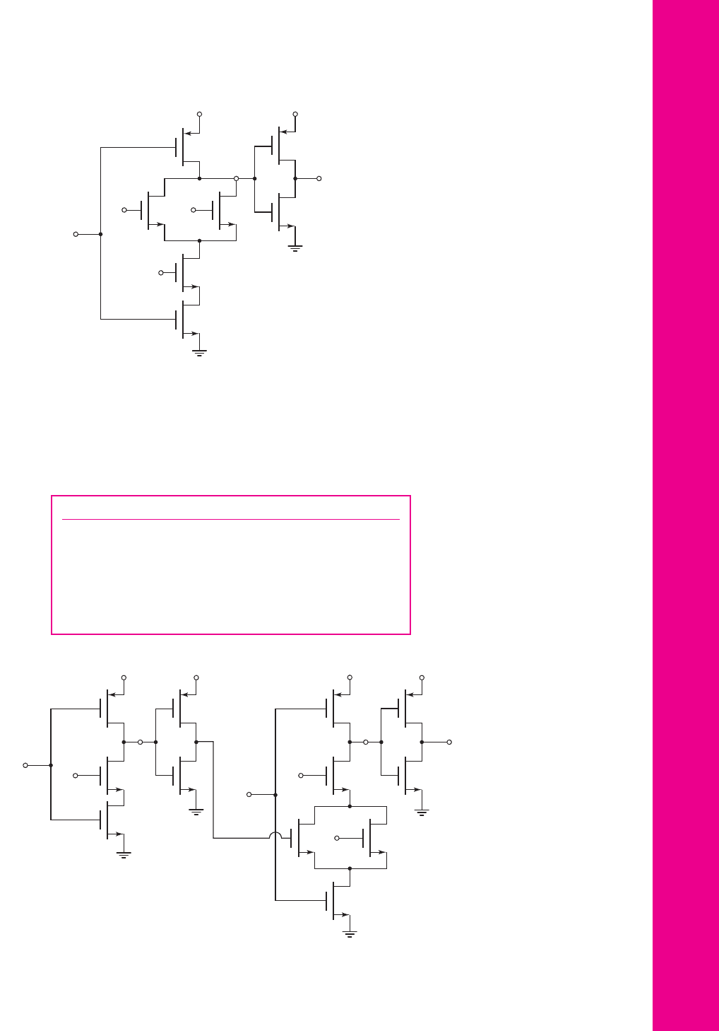
Chapter 16 MOSFET Digital Circuits 1247
V
DD
= 5 V
v
O2
v
O1
v
A
v
C
N
C
N
A
v
B
N
B
N
1
P
2
P
1
N
2
CLK
V
DD
= 5 V
Figure P16.61
16.62 (a) For the circuit in Figure P16.62, make a table showing the state of each
transistor (“on” or “off”), and determine the output voltages
v
O1
,
v
O2
, and
v
O3
for the input logic states listed in the following table. Assume the input
conditions are sequential in time from state 1 to state 6. (b) What logic func-
tion does the circuit implement?
State CLK v
X
v
Y
v
Z
10000
21111
30000
41011
50000
61101
5 V
v
O3
v
O2
v
Z
v
Y
CLK
5 V
5 V
v
O1
5 V
CLK
v
X
Figure P16.62
nea80644_ch16_1145-1254.qxd 07/12/2009 3:38 Page 1247 pinnacle MHDQ-New:MHDQ134:MHDQ134-16: