Neamen D. Microelectronics: Circuit Analysis and Design
Подождите немного. Документ загружается.


1248 Part 3 Digital Electronics
D16.63 Sketch a clocked CMOS domino logic circuit that realizes the function
Y = A
¯
B +
¯
AB
. Assume that both the variable and its complement are
available as input signals.
D16.64 Sketch a clocked CMOS domino logic circuit that realizes the function
Y = AB + C(D + E)
.
D16.65 Sketch a clocked CMOS domino logic circuit that realizes the function
Y = A(B + C)(D + E)
.
16.66 Consider the CMOS clocked circuit in Figure 16.44(b). Assume the
effective capacitance at the
v
O1
terminal is 25 fF. If the leakage current
through the
M
NA
and
M
NB
transistors is
I
Leakage
= 2pA
when these tran-
sistors and
M
P1
are cutoff, determine the time for which
v
O1
will decay
by 0.5 V.
Section 16.6 Transmission Gates
16.67 The parameters of an NMOS transmission gate are
V
TN
= 0.4
V,
K
n
= 0.15
mA/V
2
, and
C
L
= 0.2
pF. (a) For a gate voltage of
φ = 3.3
V, d e -
termine the quasi-steady-state output voltage for (i)
v
I
= 0
, (ii)
v
I
= 3.3
V,
and (iii)
v
I
= 2.5
V. (b) Repeat part (a) for a gate voltage of
φ = 1.8
V.
16.68 The NMOS transistors in the circuit shown in Figure P16.68 have parameters
K
n
= 0.2
mA/V
2
,
V
TN
= 0.5
V,
λ = 0
,and
γ = 0
. (a) For gate voltages of
φ = 2.5
V, determine the quasi-steady-state output voltage for (i)
v
I
= 0
,
(ii)
v
I
= 2.5
V, and (iii)
v
I
= 1.8
V. (b) Repeat part (a) for gate voltages of
φ = 2.0
V.
16.69 Consider the circuit shown in Figure P16.69. The input voltage
v
I
is either
0.1 V or 2.5 V. Assume gate voltages of
φ = 2.5
V. The threshold voltages
are
V
TN
=−0.6
V for
M
4
and
V
TN
= 0.4
V for all other transistors. The
width-to-length ratios are 1 for
M
2
and
M
4
, and 5 for
M
A
and
M
B
. (a) What
are the logic 1 values for
v
O1
and
v
O2
? (b) Design the width-to-length ratios
of
M
1
and
M
3
such that the logic 0 values of
v
O1
and
v
O2
are 0.1 V
16.70 Consider the circuit in Figure P16.70. What logic function is implemented
by this circuit? Are there any potential problems with this circuit?
C
L
= 1 pF
v
O
v
I
fff
Figure P16.68
v
I
v
O2
v
O1
2.5 V2.5 V
M
A
M
B
M
2
M
3
M
4
M
1
ff
Figure P16.69
nea80644_ch16_1145-1254.qxd 07/12/2009 3:38 Page 1248 pinnacle MHDQ-New:MHDQ134:MHDQ134-16:

Chapter 16 MOSFET Digital Circuits 1249
16.71 What is the logic function implemented by the circuit in Figure P16.71?
D16.72 (a) Design an NMOS pass transistor logic circuit to perform the function
Y = A + B(C + D)
. Assume that both the variable and its complement
are available as input signals. (b) Repeat part (a) for the function
Y = ABC +
¯
A
¯
B
¯
C
.
16.73 Consider the circuit in Figure P16.73. (a) Determine the value of
Y
for
φ = 2.5
V and (i)
A = B = 0
; (ii)
A = 0
,
B = 2.5
V; (iii)
A = 2.5
V,
B = 0
; and (iv)
A = B = 2.5
V. (b) Repeat part (a) for
φ = 0
. (c) What is
the logic function implemented by the circuit?
16.74 What is the logic function implemented by the circuit in Figure P16.74?
16.75 Consider the circuit in Figure P16.75. (a) Determine the value of
Y
for
(i)
A = B = 0
; (ii)
A = 2.5
V,
B = 0
; (iii)
A = 0
,
B = 2
.5
V; and
(iv)
A = B = 2.5
V. (b) What is the logic function implemented by the
circuit?
A
Y
A
0
B
–
B
–
Figure P16.70
–
Y
A
A
B
–
A
–
B
A
Z
Figure P16.71
Y
A
B
f
f
f
–
Figure P16.73
Y
C
A
B
C
–
C
–
Figure P16.74
Y
A
B
B
A
–
–
A
Figure P16.75
nea80644_ch16_1145-1254.qxd 07/12/2009 3:38 Page 1249 pinnacle MHDQ-New:MHDQ134:MHDQ134-16:
1250 Part 3 Digital Electronics
v
I
v
O
v
O1
3.3 V
Figure P16.79
Section 16.7 Sequential Logic Circuits
16.78 Consider the NMOS R-S flip-flop in Figure 16.63 biased at
V
DD
= 2.5
V.
The threshold voltages are 0.4 V (enhancement-mode devices) and
−0.6
V
(depletion-mode devices). The conduction parameters are
K
3
=
K
6
= 40 μ
A/V
2
,
K
2
= K
5
= 100 μ
A/V
2
, and
K
1
= K
4
= 150 μ
A/V
2
. If
Q =
logic 0 and
¯
Q =
logic 1 initially, determine the voltage at
S
that will
cause the flip-flop to change states.
16.79 Figure P16.79 shows two CMOS inverters in cascade. This circuit can be
thought of as an uncoupled CMOS R/S flip flop. The transistor parameters
are
K
n
= K
p
=0.2 mA/V
2
,
V
TN
=0.5V
,
V
TP
=−0.4
V, and
λ
n
=λ
p
=0
.
Plot
v
O1
and
v
O
versus
v
I
. In particular, calculate the values of
v
O1
and
v
O
at
v
I
= 1.5
, 1.6, 1.7, and 1.8 V.
16.80 Consider the circuit in Figure P16.80. Determine the state of the outputs for
various input signals. What is the purpose of the input signal
φ
?
V
DD
M
7
M
5
M
6
QQ
f
f
SR
M
1
M
2
M
4
M
3
M
8
–
Figure P16.80
B
A
A
Y
–
P
2
N
2
P
1
N
1
V
DD
Figure P16.76
v
I
f
1
f
2
v
O1
V
DD
v
O
C
L
V
DD
Figure P16.77
16.76 What is the logic function implemented by the circuit in Figure P16.76?
16.77 The circuit in Figure P16.77 is a form of clocked shift register. Signals
φ
1
and
φ
2
are nonoverlapping clock signals. Describe the operation of the
circuit. Discuss any possible relationship between the width-to-length ratios
of the load and driver transistors for “proper” circuit operation.
nea80644_ch16_1145-1254.qxd 07/12/2009 3:38 Page 1250 pinnacle MHDQ-New:MHDQ134:MHDQ134-16:
Chapter 16 MOSFET Digital Circuits 1251
D
V
DD
Q
M
3
M
1
M
5
CLK
M
4
M
2
Figure P16.81
CLK
CLK
D
Q
Q
K
J
S
D
V
DD
R
D
–
Figure P16.82
D16.81 The circuit in Figure P16.81 is an example of a D flip-flop. (a) Explain the
operation of the circuit. Is this a positive- or negative-edge-triggered flip-
flop? (b) Redesign the circuit to make this a static flip-flop.
16.82 Show that the circuit in Figure P16.82 is a J–K flip-flop.
16.83 Reconsider the circuit shown in Figure P16.48. Show that this circuit is a
J–K flip-flop with
J = v
X
,
K = v
Y
, and
CLK = v
Z
.
Section 16.8 Memories: Classifications and Architectures
16.84 A 256-K memory is organized in a square array and uses the NMOS NOR
decoder in Figure 16.73(b) for the row- and column-decoders. (a) How
many inputs does each decoder require? (b) What input to the row decoder
is required to address row (i) 52, (ii) 129, and (iii) 241? (c) What input to the
column decoder is required to address column (i) 24, (ii) 165, and (iii) 203?
nea80644_ch16_1145-1254.qxd 07/12/2009 3:38 Page 1251 pinnacle MHDQ-New:MHDQ134:MHDQ134-16:

1252 Part 3 Digital Electronics
16.85 (a) A 1 megabit memory is organized in a square with each memory cell
being individually addressed. Determine the number of input address lines
required for the row and column decoders. (b) If the 1 megabit memory is
organized as 250K words
× 4
bits, determine the minimum number of input
address lines required for the row and column decoders.
16.86 A 4096-bit RAM consists of 512 words of 8 bits each. Design the
memory array to minimize the number of row and column address
decoder transistors required. How many row and column address lines
are required?
16.87 Assume that an NMOS address decoder can source 250
μ
A when the output
goes high. If the effective capacitance of each memory cell is
C
L
= 0.8pF
and the effective capacitance of the address line is
C
LA
= 5pF
, determine
the rise time of the address line voltage if
V
IH
= 2.7V
.
Section 16.9 RAM Memory Cells
16.88 Consider the NMOS RAM cell with resistor load in Figure 16.74(b).
Assume parameters values of
k
n
= 80 μ
A/V
2
,
V
TN
= 0.4
V,
V
DD
= 2.5
V,
and
R = 1
M
. (a) Design the width-to-length ratio of the driver transistor
such that
V
DS
= 20
mV for the on transistor. (b) Consider a 16-K memory
with the cell described in part (a). Determine the standby cell current and
the total memory power dissipation for a standby voltage of
V
DD
= 1.2
V.
D16.89 A 16-K NMOS RAM, with the cell design shown in Figure 16.74(b), is to
dissipate no more than 200 mW in standby when biased at
V
DD
= 2.5V
.
Design the width-to-length ratios of the transistors and the resistance value.
Assume
V
TN
= 0.7V
and
k
n
= 35 μA/V
2
.
16.90 Consider the CMOS RAM cell and data lines in Figure 16.76 biased at
V
DD
= 2.5
V. Assume transistor parameters
k
n
= 80 μ
A/V
2
,
k
p
= 35 μ
A/V
2
,
V
TN
= 0.4
V,
V
TP
=−0.4
V,
W/L = 2
(
M
N1
and
M
N2
)
,
W/L = 4
(
M
P1
and
M
P2
)
, and
W/L = 1
(all other transistors). If
Q = 0
and
¯
Q = 1
, deter-
mine the steady-state values of
D
and
¯
D
after the row has been selected.
Neglect the body effect.
16.91 Consider the CMOS RAM cell and data lines in Figure 16.76 with circuit
and transistor parameters described in Problem 16.90. Assume initially that
Q = 0
and
¯
Q = 1
. Assume the row is selected with
X = 2.5
V and assume
the data lines, through a write cycle, are
¯
D = 0
and
D = 2.5
V. Determine
the values of
Q
and
¯
Q
just after the row select has been applied.
*16.92 Consider a general sense amplifier configuration shown in Figure 16.82
for a dynamic RAM. Assume that each bit line has a capacitance of 1 pF
and is precharged to 4 V. The storage capacitance is 0.05 pF, the reference
capacitance is 0.025 pF, and each is charged to 5 V for a logic 1 and to 0 V
for a logic 0. The
M
S
and
M
R
gate voltages are 5 V when each cell is
addressed and the transistor threshold voltages are 0.5 V. Determine the
bit line voltages
v
1
and
v
2
after the cells are addressed for the case when
(a) a logic 1 is stored and (b) a logic 0 is stored.
Section 16.10 Read-Only Memory
D16.93 Design a 4-word
×
4-bit NMOS mask-programmed ROM to produce outputs
of 1011, 1111, 0110, and 1001 when rows 1, 2, 3, and 4, respectively, are
addressed.
nea80644_ch16_1145-1254.qxd 07/12/2009 3:38 Page 1252 pinnacle MHDQ-New:MHDQ134:MHDQ134-16:

Chapter 16 MOSFET Digital Circuits 1253
D16.94 Design an NMOS
16 × 4
mask-programmed ROM that provides the 4-bit
product of two 2-bit variables.
D16.95 Design an NMOS mask-programmed ROM that decodes a binary input and
produces the output for a seven-segment array. (See Figure 2.45, Chapter 2.)
The output is to be high when a particular LED is to be turned on.
Section 16.11 Data Converters
16.96 An analog signal in the range 0 to 5 V is to be converted to a digital signal
with a quantization error of less than one percent. (a) What is the required
number of bits? (b) What input voltage value represents 1 LSB? (c) What
digital output represents an input voltage of 3.5424 V?
16.97 An analog signal in the range 0 to 3.3 V is to be converted to a digital signal
with a quantization error of less than 0.5 percent. (a) What is the required
number of bits? (b) What input voltage value represents 1 LSB? (c) What
digital output represents an input voltage of 2.5321 V.
16.98 (a) What is the output voltage of the 4-bit weighted-resistor D/A in Figure
16.90 if the input is 0110? Assume
R
F
= 10
k
. (b) The input signal
changes to 1001. What is the output voltage?
16.99 Consider the 4-bit weighted-resistor D/A converter in Figure 16.90. Let
R
F
= 10 k
. (a) What is the maximum allowed tolerance (
±
percent) in the
value of
R
1
so that the maximum error in the output is limited to
±
1
2
LSB?
(b) Repeat part (a) for the resistor
R
4
.
16.100 The weighted-resistor D/A converter in Figure 16.90 is to be expanded to an 8-
bit device. (a) What are the required resistance values of the additional four
input resistors? (b) What is the output voltage if the input is 00000001?
16.101 The N-bit D/A converter with an R–2R ladder network in Figure 16.92 is to
be designed as a 6-bit D/A device. Let
V
REF
=−5.0V
and
R = R
F
=
5.0k
. (a) What are currents
I
1
, I
2
, I
3
, I
4
, I
5
, and
I
6
? (b) The input changes
by 1 LSB. What is the change in the output voltage? (c) What is the output
voltage if the input is 010011? (d) What is the change in output voltage if
the input changes from 101010 to 010101?
16.102 The 3-bit flash A/D converter in Figure 16.93 has a reference voltage of
V
REF
= 3.3
V. The 3-bit output is 101. What is the range of
v
A
that produces
this output?
16.103 A 6-bit flash A/D converter, similar to the one in Figure 16.93, is to be fab-
ricated. How many resistors and comparators are required?
16.104 A 10-bit counting A/D converter has an analog input in the range
0 ≤v
A
≤
5 V and has a clock frequency of 1 MHz. (a) What is the maximum conver-
sion time? (b) If the output is 0010010010, what is the range of the input
signal
v
A
(assume a quantization error of
±
1
2
LSB). (c) How many clock
pulses are required to produce an output of 0100100100?
16.105 Consider the 10-bit counting A/D converter described in Problem 16.104.
(a) What is the output if the analog input is
v
A
= 3.125 V
? (b) Repeat
part (a) if
v
A
= 1.8613 V
.
COMPUTER SIMULATION PROBLEMS
16.106 Consider the three types of NMOS inverters shown in Figures 16.3(a),
16.5(a), and 16.7(a). Using a computer simulation, investigate the voltage
transfer characteristics and the current versus input voltage characteristics
nea80644_ch16_1145-1254.qxd 07/15/2009 09:33 PM Page 1253 F506 Hard disk:Desktop Folder:ALI-07-15-09:

1254 Part 3 Digital Electronics
of the three types of inverters as a function of various width-to-length ratios
and as a function of the body effect.
16.107 Using a computer simulation, investigate the propagation delay time and
switching characteristics of a CMOS inverter by setting up a series of
CMOS inverters in cascade. Use standard transistors and assume effective
C
T
load capacitances of 0.05 pF. Determine the propagation delay time as a
function of various transistor width-to-length ratios.
16.108 Consider a three-input CMOS NAND logic circuit similar to the two-input
circuit shown in Figure 16.34(a). Using a computer simulation, investigate
the voltage transfer characteristics and switching characteristics for various
NMOS and PMOS width-to-length ratios. What is the optimum relation be-
tween the PMOS and NMOS width-to-length ratios for symmetrical switch-
ing speeds?
16.109 Using a computer simulation, investigate the
Q
and
¯
Q
values in the CMOS
RAM cell shown in Figure 16.76 during read and write cycles for various
transistor width-to-length ratios. In particular, consider the relations given
by Equations (16.82) and (16.84).
DESIGN PROBLEMS
D16.110 Design a classic CMOS logic circuit that will implement the logic function
Y = A ·
(
B + C
)
+ D · E
.
D16.111 Design clocked CMOS logic circuits that will implement the logic func-
tions (a)
Y =
[
A · B + C · D
]
and (b)
Y =
[
A ·
(
B + C
)
+ D
]
.
D16.112 Design an NMOS pass logic network that implements the logic functions
described in Problem 16.111.
D16.113 Design a clocked CMOS dynamic shift register in which the output
becomes valid on the positive-going edge of a clock signal.
*
**
*
*
nea80644_ch16_1145-1254.qxd 07/12/2009 3:38 Page 1254 pinnacle MHDQ-New:MHDQ134:MHDQ134-16:

Chapter
Bipolar Digital
Circuits
1255
In the previous chapter, we presented the basic concepts of MOSFET logic circuits.
In this chapter, we discuss the basic principles of bipolar logic circuits. We initially
consider emitter-coupled logic (ECL). This technology is based on the differential
amplifier and is used in specialized high-speed applications.
Prior to the emergence of MOS digital technology, the bipolar digital family of
transistor–transistor logic (TTL) circuits was used extensively. TTL and low-power
Schottky TTL logic circuits are analyzed. The basic concepts of BiCMOS logic cir-
cuits are presented.
Bipolar digital circuits are now used less frequently because of their relatively
large power requirements.
PREVIEW
In this chapter, we will:
• Analyze the basic emitter-coupled logic circuits.
• Analyze and design modified emitter-coupled logic circuits.
• Analyze transistor–transistor logic circuits.
• Analyze and design Schottky and low-power Schottky transistor–transistor
logic circuits.
• Analyze BiCMOS digital logic circuits.
• As an application, design a static ECL gate to implement a specific logic
function.
17
17
nea80644_ch17_1255-1314.qxd 6/8/09 08:53 PM Page 1255 Aptara Inc.
1256 Part 3 Digital Electronics
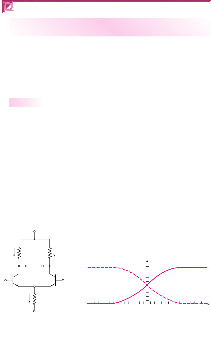
1
In most cases in this chapter, total instantaneous current and voltage parameters are used, even though
most analyses of logic circuits involve dc calculations.
v
O2
v
O1
v
1
v
2
v
E
R
E
R
C2
R
C1
V
+
V
–
++
–
–
v
BE1
Q
1
Q
2
v
BE2
i
C2
i
C1
i
E
Figure 17.1 Basic
differential amplifier circuit
17.1 EMITTER-COUPLED LOGIC (ECL)
Objective: • Analyze the basic emitter-coupled logic circuits
The emitter-coupled logic (ECL) circuit is based on the differential amplifier circuit,
which we studied in Chapter 11 in the context of linear amplifiers. In digital applica-
tions, the diff-amp is driven into its nonlinear region. The transistors are either cut off
or in the active region. Saturation is avoided in order to minimize switching times
and propagation delay times. ECL circuits have the shortest propagation delay times
of any bipolar digital technology.
Differential Amplifier Circuit Revisited
Consider the basic diff-amp circuit in Figure 17.1. For a linear diff-amp, the differ-
ence between the two input voltages is small and both transistors remain biased
in the active region at all times. The relationship between collector currents and
base–emitter voltages for
Q
1
and
Q
2
can be written
1
i
C1
= I
S
e
v
BE1
/V
T
(17.1(a))
and
i
C2
= I
S
e
v
BE2
/V
T
(17.1(b))
where
Q
1
and
Q
2
are assumed to be matched and parameter
I
S
is the same for both
devices. The current–voltage transfer curves are shown in Figure 17.2.
In digital applications, the difference between the two input voltages is large,
which means that one transistor remains biased in its active region while the opposite
17.1.1
v
d
= v
BE1
– v
BE2
(volts)
0 0.05
0.5
1.0
0.10 0.15
–
0.15 – 0.10 – 0.05
i
C1
/I
Q
i
C2
/I
Q
Figure 17.2 Normalized dc transfer characteristics, BJT
differential amplifier
nea80644_ch17_1255-1314.qxd 8/6/09 11:11 AM Page 1256 pmath DATA-DISK:Desktop Folder:UDAYVEER/Neamen:

Chapter 17 Bipolar Digital Circuits 1257
transistor is cut off. For example, if
v
BE1
= v
BE2
+0.12
, then the ratio of
i
C1
and
i
C2
is
i
C1
i
C2
=
e
v
BE1
/V
T
e
v
BE2
/V
T
= e
(v
BE1
−v
BE2
)/V
T
= e
0.12/0.026
= 101
(17.2)
When the base–emitter voltage of
Q
1
is 120 mV greater than the base–emitter volt-
age of
Q
2
, the collector current of
Q
1
is 100 times that of
Q
2
; for all practical
purposes,
Q
1
is on and
Q
2
is cut off.
Conversely, if
v
1
is less than
v
2
by at least 120 mV, then
Q
1
is effectively cut off and
Q
2
is on. The difference amplifier, when operating as a digital circuit, operates as a cur-
rent switch. When
v
1
>v
2
by at least 120 mV, it switches an approximately constant
current through
R
E
to
Q
1
; when
v
2
>v
1
by at least 120 mV, the current goes to
Q
2
.
EXAMPLE 17.1
Objective: Calculate the currents and voltages in the basic differential amplifier
circuit used as a digital circuit.
Consider the circuit in Figure 17.1. Assume that
V
+
= 2.5
V,
V
−
=−2.5
V,
R
C1
= R
C2
≡ R
C
= 5
k
,
R
E
= 6
k
, and
v
2
= 0
. Neglect base currents in the dc
analysis.
Solution: For
v
1
= v
2
= 0
, both transistors are on. Assume a base–emitter turn-on
voltage of 0.7 V; then
v
E
=−0.7
V and
i
E
=
v
E
− V
−
R
E
=
−0.7 − (−2.5)
6
= 0.3mA
Assuming
Q
1
and
Q
2
are matched, we have
i
C1
= i
C2
= i
E
/2
so that
i
C1
= i
C2
=
0.15
mA. Then
v
O1
= v
O2
= V
+
−i
C
R
C
= 2.5 −(0.15)(5) = 1.75 V
Both
Q
1
and
Q
2
are biased in the active region.
Now let
v
1
=−0.5
V. Since the base voltage of
Q
1
is less than the base voltage
of
Q
2
by more than 120 mV, then
Q
1
is cut off and
Q
2
is on. In this case,
v
E
= v
2
− V
BE
(on) =−0.7
V and
i
E
= 0.3
mA, as before. However,
i
C1
= 0
and
i
C2
= i
E
= 0.3
mA, so that
v
O1
= V
+
= 2.5
V
and
v
O2
= V
+
−i
C2
R
C
= 2.5 −
(
0.3
)(
5
)
= 1.0
V
For
v
1
=+0.5
V,
Q
1
is on and
Q
2
is cut off. For this case,
v
E
= v
1
− V
BE
(on) = 0.5 −0.7 =−0.2
V and the current
i
E
is
i
E
= i
C1
=
v
E
− V
−
R
E
=
−0.2 − (−2.5)
6
= 0.383 mA
Then
v
O1
= V
+
−i
C1
R
C
= 2.5 −
(
0.383
)(
5
)
= 0.585
V
and
v
O2
= V
+
= 2.5
V
nea80644_ch17_1255-1314.qxd 8/6/09 11:12 AM Page 1257 pmath DATA-DISK:Desktop Folder:UDAYVEER/Neamen: