Neamen D. Microelectronics: Circuit Analysis and Design
Подождите немного. Документ загружается.

1258 Part 3 Digital Electronics
Comment: For the three conditions given, transistors
Q
1
and
Q
2
are biased either in
cutoff or in the active region. In terms of digital applications, output
v
O2
is in phase
with input
v
1
and output
v
O1
is 180 degrees out of phase.
When biased on, transistor
Q
1
conducts slightly more heavily than
Q
2
when it
is conducting. To obtain symmetrical complementary outputs,
R
C1
should therefore
be slightly smaller than
R
C2
.
EXERCISE PROBLEM
Ex 17.1: Consider the differential amplifier circuit in Figure 17.1 biased at
V
+
=
1.8
V,
V
−
=−1.8
V, and
v
2
= 0
. Assume
V
BE
(on) = 0.7
V and neglect base
currents. (a) Design the circuit such that
i
E
= 0.11
mA and
v
O1
= v
O2
= 1.45
V
when
v
1
= 0
. (b) Using the results of part (a), determine
i
E
,
v
O1
, and
v
O2
for (i)
v
1
=+0.5
V and (ii)
v
1
=−0.5
V. (c) Using the results of parts (a) and (b), cal-
culate the power dissipated in the circuit for (i)
v
1
=+0.5
V and (ii)
v
1
=−0.5
V.
(Ans. (a)
R
E
= 10
k
,
R
C
= 6.364
k
; (b) (i)
i
E
= 0.16
mA,
v
O1
= 0.782
V,
v
O2
= 1.8
V; (ii)
i
E
= 0.11
mA,
v
O1
= 1.8
V,
v
O2
= 1.10
V; (c) (i)
P =0.576
mW,
(ii)
P = 0.396
mW)
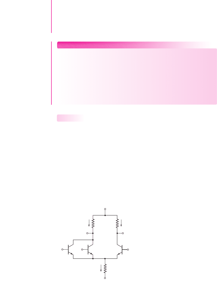
Basic ECL Logic Gate
Basic ECL Logic Gate
A basic two-input ECL OR/NOR logic circuit is shown in Figure 17.3. The two input
transistors,
Q
1
and
Q
2
, are connected in parallel. On the basis of the differential
amplifier, if both
v
X
and
v
Y
are less than the reference voltage
V
R
(by at least
120 mV), then both
Q
1
and
Q
2
are cut off, while the reference transistor
Q
R
is biased
on its active region. In this situation, the output voltage
v
O1
is greater than
v
O2
. If
either
v
X
or
v
Y
becomes greater than
V
R
, then
Q
R
turns off and
v
O2
becomes larger
than
v
O1
. The OR logic is at the
v
O2
output and the NOR logic is at the
v
O1
output.
An advantage of ECL gates is the availability of complementary outputs, precluding
the need for separate inverters to provide the complementary outputs.
One problem with the OR/NOR circuit in Figure 17.3 is that the output voltage
levels differ from the required input voltage levels; the output voltages are not
17.1.2
v
O2
v
O1
v
Y
v
X
V
R
R
E
R
C2
R
C1
V
+
V
–
Q
1
Q
2
Q
R
i
CR
i
CXY
i
E
Figure 17.3 Basic two-input ECL OR/NOR logic circuit
nea80644_ch17_1255-1314.qxd 8/6/09 11:12 AM Page 1258 pmath DATA-DISK:Desktop Folder:UDAYVEER/Neamen:
Chapter 17 Bipolar Digital Circuits 1259
compatible with the input voltages. The mismatch arises because ECL circuit
transistors operate between their cutoff and active regions, requiring that the
base–collector junctions be reverse biased at all times. We see that a logic 1 voltage
of the output is
V
OH
= V
+
. If this voltage were to be applied to either the
v
X
or
v
Y
input, then either
Q
1
or
Q
2
would turn on and the collector voltage
v
O1
would
decrease below
V
+
; the base–collector voltage would then become forward biased
and the transistor would go into saturation. Emitter-follower circuits are added to
provide outputs that are compatible with the inputs of similar gates.
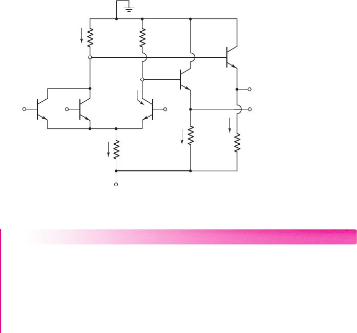
ECL Logic Gate with Emitter Followers
In the ECL circuit in Figure 17.4, emitter followers are added to the OR/NOR outputs,
and supply voltage
V
+
is set equal to zero. The ground and power supply voltages are
reversed because analyses show that using the collector–emitter voltage as the output re-
sults in less noise sensitivity. If the forward current gain of the transistors is on the order
of 100, then the dc base currents may be neglected with little error in the calculations.
If either
v
X
or
v
Y
is a logic 1 (defined as greater than
V
R
by at least 120 mV), then
the reference transistor
Q
R
is cut off,
i
CR
= 0
, and
v
O2
= 0
. Output transistor
Q
3
is bi-
ased in the active region, and
v
OR
= v
O2
− V
BE
(on) =−0.7V
. If both
v
X
and
v
Y
are
a logic 0 (defined as less than
V
R
by at least 120 mV), then both
Q
1
and
Q
2
are cut off,
v
O1
= 0
, and
v
NOR
= 0 − V
BE
(on) =−0.7V
. The largest possible voltage that can
be achieved at either output is
−0.7V
; therefore,
−0.7V
is defined as the logic 1 level.
In the following example, we will determine the currents and the logic 0 values
in the basic ECL gate.
v
O2
v
O1
v
Y
v
X
V
R
R
E
=
1.18 kΩ
R
C2
R
3
=
1.5 kΩ
R
4
=
1.5 kΩ
R
C1
V
–
= –5.2 V
v
NOR
v
OR
Q
1
Q
2
Q
R
i
CXY
i
E
i
3
i
CR
i
4
Q
4
Q
3
Figure 17.4 Two-input ECL OR/NOR logic gate with emitter-follower output stages
EXAMPLE 17.2
Objective: Calculate current, resistor, and logic 0 values in the basic ECL logic gate.
Consider the circuit in Figure 17.4. Determine
R
C1
and
R
C2
such that when
Q
1
and
Q
2
are conducting, the B–C voltages are zero.
Solution: Let
v
X
= v
Y
=−0.7V= logic 1 > V
R
such that
Q
1
and
Q
2
are on. We
find that
v
E
= v
X
− V
BE
(on) =−0.7 −0.7 =−1.4V
nea80644_ch17_1255-1314.qxd 8/6/09 11:12 AM Page 1259 pmath DATA-DISK:Desktop Folder:UDAYVEER/Neamen:

1260 Part 3 Digital Electronics
and the current is
i
E
= i
Cxy
=
v
E
− V
−
R
E
=
−1.4 − (−5.2)
1.18
= 3.22 mA
In order for the B–C voltages of
Q
1
and
Q
2
to be zero, voltage
v
O1
must be
−0.7V
.
Therefore
R
C1
=
−v
O1
I
Cxy
=
0.7
3.22
= 0.217 k
The NOR output logic 0 value is then
v
NOR
= v
O1
− V
BE
(on) =−0.70 −0.7 =−1.40 V
Input voltages
v
X
and
v
Y
are greater than
V
R
in a logic 1 state and less than
V
R
in a logic 0 state. If
V
R
is set at the midpoint between the logic 0 and logic 1 levels,
then
V
R
=
−0.7 − 1.40
2
=−1.05 V
When
Q
R
is on, we have
v
E
= V
R
− V
BE
(on) =−1.05 −0.7 =−1.75 V
and
i
E
= i
CR
=
v
E
− V
−
R
E
=
−1.75 − (−5.2)
1.18
= 2.92 mA
For
v
O2
=−0.7V
, we find that
R
C2
=
−v
O2
i
C2
=
0.7
2.92
= 0.240 k
The OR logic 0 value is therefore
v
OR
= v
O2
− V
BE
(on) =−0.7 −0.7 =−1.40 V
Comment: For symmetrical complementary outputs,
R
C1
and
R
C2
are not equal. If
R
C1
and
R
C2
become larger than the designed values, transistors
Q
1
,
Q
2
, and
Q
R
will be driven into saturation when they are conducting.
EXERCISE PROBLEM
Ex 17.2: Using the results of Example 17.2, calculate the power dissipated in the
circuit in Figure 17.4; for: (a)
v
x
= v
y
= logic 1
, and (b)
v
x
= v
y
= logic 0
. (Ans.
(a)
P = 45.5mW
(b)
P = 43.9mW
)
The Reference Circuit
Another circuit is required to provide the reference voltage
V
R
. Consider the com-
plete two-input ECL OR/NOR logic circuit shown in Figure 17.5. The reference cir-
cuit consists of resistors
R
1
,
R
2
, and
R
5
, diodes
D
1
and
D
2
, and transistor
Q
5
. The
reference portion of the circuit can be specifically designed to provide the desired
reference voltage.
nea80644_ch17_1255-1314.qxd 8/6/09 11:12 AM Page 1260 pmath DATA-DISK:Desktop Folder:UDAYVEER/Neamen:
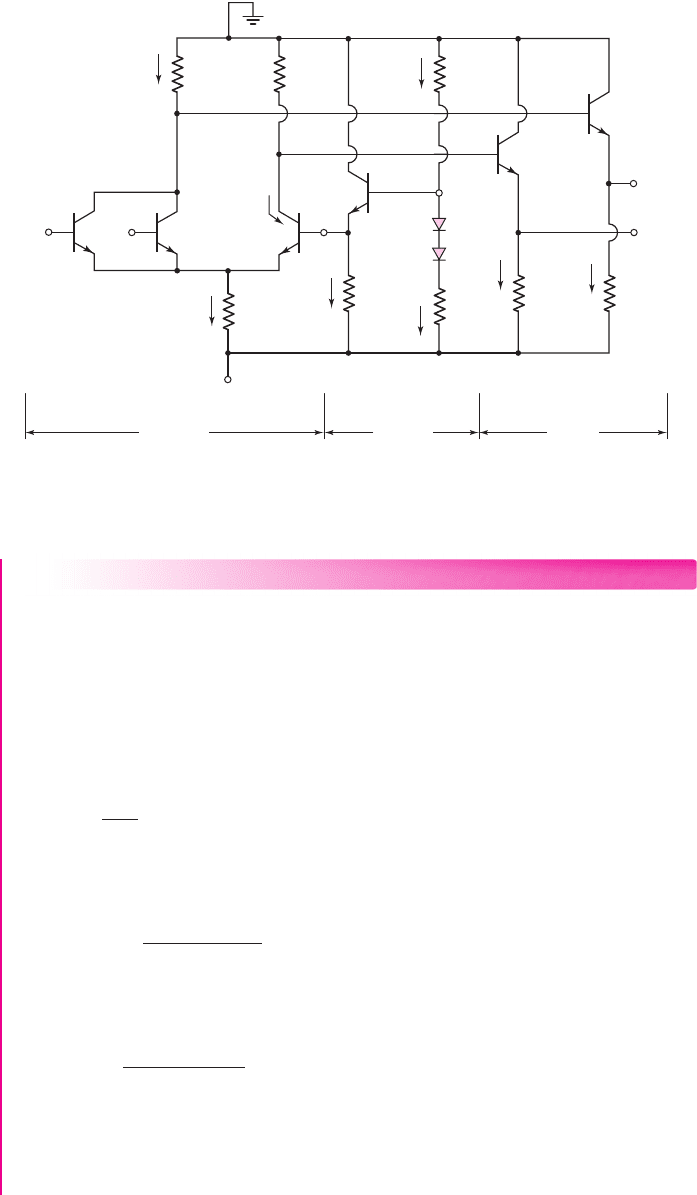
Chapter 17 Bipolar Digital Circuits 1261
v
B5
v
Y
v
X
V
R
D
1
D
2
R
E
=
1.18 kΩ
R
3
=
1.5 kΩ
R
4
=
1.5 kΩ
R
C1
=
217 Ω
V
–
= –5.2 V
v
NOR
v
OR
Q
1
Q
2
Q
R
Q
5
i
CXY
i
E
i
3
R
2
=
2.46 kΩ
i
2
R
1
=
250 Ω
R
C2
=
240 Ω
i
1
R
5
=
2.96 kΩ
i
5
i
CR
i
4
Q
4
Q
3
Reference
voltage
circuit
Level
shifters
Difference
amplifier
Figure 17.5 Basic ECL logic gate with reference circuit
DESIGN EXAMPLE 17.3
Objective: Design the reference portion of the ECL circuit.
Consider the circuit in Figure 17.5. The reference voltage
V
R
is to be
−1.05 V
.
Solution: We know that
v
B5
= V
R
+ V
BE
(on) =−1.05 +0.7 =−0.35 V =−i
1
R
1
Since there are two unknowns, we will choose one variable. Let
R
1
= 0.25 k
.
Then,
i
1
=
0.35
0.25
= 1.40 mA
Since this current is on the same order of magnitude as other currents in the circuit,
the chosen value of
R
1
is reasonable. Neglecting base currents, we can now write
i
1
= i
2
=
0 − 2V
γ
− V
−
R
1
+ R
2
where
V
γ
is the diode turn-on voltage and is assumed to be
V
γ
= 0.7V
. We then
have
1.40 =
−1.4 − (−5.2)
R
1
+ R
2
which yields
R
1
+ R
2
= 2.71 k
Since
R
1
= 0.25 k
, resistance
R
2
is
R
2
= 2.46 k
.
nea80644_ch17_1255-1314.qxd 8/6/09 11:12 AM Page 1261 pmath DATA-DISK:Desktop Folder:UDAYVEER/Neamen:

1262 Part 3 Digital Electronics
Also, we know that
i
5
=
V
R
− V
−
R
5
If we let
i
5
= i
1
= i
2
= 1.40 mA
, then
R
5
=
V
R
− V
−
i
5
=
−1.05 − (−5.2)
1.40
= 2.96 k
Comment: As with any design, there is no unique solution. The design presented
will provide the required reference voltage to the base of
Q
R
.
EXERCISE PROBLEM
Ex 17.3: The reference circuit in Figure 17.5 is to be redesigned with
V
+
= 0
and
V
−
=−3.3
V. The reference voltage is to be
V
R
=−1.0
V and the currents are to
be
i
1
= i
2
= i
5
= 0.5
mA. (Ans.
R
1
= 0.6
k
,
R
2
= 3.2
k
,
R
5
= 4.6
k
)
ECL Logic Circuit Characteristics
In this section, we will determine the power dissipation, fanout, and propagation
delay times for the ECL logic gate. We will also examine the advantage of using a
negative power supply.
Power Dissipation
Power dissipation is an important characteristic of a logic circuit. The power dissi-
pated in the basic ECL logic gate in Figure 17.5 is given by
P
D
= (i
Cxy
+i
CR
+i
5
+i
1
+i
3
+i
4
)(0 − V
−
)
(17.3)
EXAMPLE 17.4
Objective: Calculate the power dissipated in the ECL logic circuit.
Consider the circuit in Figure 17.5. Let
v
X
= v
Y
=−0.7V= logic 1
.
Solution: From our previous analysis, we have
i
Cxy
= 3.22 mA
,
i
CR
= 0
,
i
5
=
1.40 mA
, and
i
1
= 1.40 mA
, and the output voltages are
v
OR
=−0.7V
and
v
NOR
=
−1.40 V
. The currents
i
3
and
i
4
are
i
3
=
v
OR
− V
−
R
3
=
−0.7 − (−5.2)
1.5
= 3.0mA
and
i
4
=
v
NOR
− V
−
R
4
=
−1.40 − (−5.2)
1.5
= 2.53 mA
The power dissipation is then
P
D
= (3.22 +0 +1.40 + 1.40 +3.0 + 2.53)(5.2) = 60.0mW
Comment: This power dissipation is significantly larger than that in NMOS and
CMOS logic circuits. The advantage of ECL, however, is the short propagation delay
times, which can be less than 1 ns.
17.1.3
nea80644_ch17_1255-1314.qxd 8/6/09 11:12 AM Page 1262 pmath DATA-DISK:Desktop Folder:UDAYVEER/Neamen:
Chapter 17 Bipolar Digital Circuits 1263
EXERCISE PROBLEM
Ex 17.4: Assume the maximum currents in
Q
3
and
Q
4
of the ECL circuit in
Figure 17.5 are to be 1.0 mA. (a) What are the required values of
R
3
and
R
4
?
(b) Using the results of part (a), calculate the new power dissipated in the circuit
for
v
X
= v
Y
=−0.7V
. (Ans. (a)
R
3
= R
4
= 4.5k
, (b)
P = 40.8mW
)
Propagation Delay Time
The major advantage of ECL circuits is their small propagation delay time, on the
order of 1 ns or less. The two reasons for the short propagation delay times are:
(1) the transistors are not driven into saturation, which eliminates any charge storage
effects; and (2) the logic swing in the ECL logic gate is small (about 0.7 V), which
means that the voltages across the output capacitances do not have to change as much
as in other logic circuits. Also, the currents in the ECL circuit are relatively large,
which means that these capacitances can charge and discharge quickly. However, the
trade-offs for the small propagation delay time are higher power dissipation and
smaller noise margins.
ECL circuits are very fast, and they require that special attention be paid to trans-
mission line effects. Improperly designed ECL circuit boards can experience ringing
or oscillations. These problems have less to do with the ECL circuits than with the
interconnections between the circuits. Care must therefore be taken to terminate the
signal lines properly.
Fanout
Figure 17.6 shows the emitter-follower output stage of the OR output of an ECL
circuit used to drive the diff-amp input stage of an ECL load circuit. When
v
OR
is a
logic 0, input load transistor
Q
1
is cut off, effectively eliminating any load current
from the driver output stage. With
v
OR
at a logic 1 level, the input load transistor is
v
OR
v
B3
R
E
=
1.18 kΩ
R
3
=
1.5 kΩ
217 Ω
Q
1
′
Q
R
′
V
R
′
v
E
′
i
E
′
i
L
′
i
L
i
3
R
C2
=
240 Ω
240 Ω
Q
3
To N – 1, identical
load circuits
V
–
= –5.2 V
V
–
= –5.2 V
i
B3
Figure 17.6 Output stage of ECL logic gate driving N identical ECL input stages
nea80644_ch17_1255-1314.qxd 8/6/09 11:12 AM Page 1263 pmath DATA-DISK:Desktop Folder:UDAYVEER/Neamen:

1264 Part 3 Digital Electronics
on and an input base current
i
L
exists. (Up to this point, we have neglected dc base
currents; however, they are not zero.) The load current must be supplied through
Q
3
,
whose base current is supplied through
R
C2
. As the load current
i
L
increases with the
addition of more load circuits, a voltage drop occurs across
R
C2
and the output volt-
age decreases. The maximum fanout is determined partially by the maximum ampli-
tude that the output voltage is allowed to drop from its ideal logic 1 value.
EXAMPLE 17.5
Objective: Calculate the maximum fanout of an ECL logic gate, based on dc load-
ing effects.
Consider the circuit in Figure 17.6. Assume the current gain of the transistors is
β = 50
, which represents a worst-case scenario. Assume that the logic 1 level at the
OR output is allowed to decrease by 50 mV at most from a value of
−0.70 V
to
−0.75 V
.
Solution: From the figure, we see that
i
E
=
v
OR
− V
BE
(on) − V
−
R
E
=
−0.75 − 0.7 −(−5.2)
1.18
= 3.18 mA
The input base current to the load transistor is
i
B
=
i
E
(1 + β)
=
3.18
51
⇒ 62.3 μA = i
L
The total load current is therefore
i
L
= Ni
L
.
The base current
i
B3
required to produce both the load current
i
L
and current
i
3
is
i
B3
=
i
3
+i
L
(1 + β)
=
0 − v
B3
R
C2
=
0 − (v
OR
+ V
BE
(on))
R
C2
(17.4)
Also, from the figure we see that
i
3
=
v
OR
− V
−
R
3
=
−0.75 − (−5.2)
1.5
= 2.967 mA
From Equation (17.4), the maximum fanout for this condition is
2.967 + N(0.0623)
51
=
0 − (−0.75 +0.7)
0.24
which yields
N = 122
. The value of N must be rounded to the next lower integer.
Comment: This maximum fanout is based on dc conditions and is unrealistic. In
practice, the maximum fanout for ECL circuits is determined by the propagation
delay time. Each load circuit increases the load capacitance by approximately 3 pF.
A maximum fanout of about 15 is usually recommended to keep the propagation
delay time within specified limits.
EXERCISE PROBLEM
*Ex 17.5: If the fanout for the situation described in Example 17.5 is limited to
N = 10
, how much does the OR output change from the no-load value of
−0.70 V
? (Ans.
v
OR
=−0.7170 V
)
nea80644_ch17_1255-1314.qxd 8/6/09 11:12 AM Page 1264 pmath DATA-DISK:Desktop Folder:UDAYVEER/Neamen:
Chapter 17 Bipolar Digital Circuits 1265
The Negative Supply Voltage
In classic ECL circuits, it is common practice to ground the positive terminal of the
supply voltage, reducing the noise signals at the output terminal. Figure 17.7(a) shows
an emitter-follower output stage with the supply voltage
V
CC
in series with a noise
source
V
n
. The noise signal may be induced by the effect of switching currents inter-
acting with parasitic inductances and capacitances. The output voltage is measured
with respect to ground; therefore, if the positive terminal of
V
CC
is grounded, voltage
V
o
is taken as the output voltage. If the negative terminal of
V
CC
is at ground, then
V
o
is the output voltage.
To determine the effect of the noise voltage at the output, we assume that
Q
R
is
cut off, and we evaluate the small-signal hybrid-
π
equivalent circuit shown in Fig-
ure 17.7(b).
i
B3
i
3
1.5 kΩ
0.24 kΩ
Q
3
+
–
V
o
′
V
o
′
+
–
V
CC
V
n
+
–
V
o
Q
R
I
b3
g
m3
V
p 3
=
bI
b3
R
3
=
1.5 kΩ
R
C2
=
0.24 kΩ
+
–
+
–
V
p 3
V
n
+
–
V
o
r
p 3
(a) (b)
+
–
+
–
Figure 17.7 (a) Equivalent circuit, ECL emitter-follower output stage and noise generator,
and the (b) small-signal hybrid-
π
equivalent circuit
EXAMPLE 17.6
Objective: Determine the effect of a noise signal on the output of an ECL gate.
Consider the small-signal equivalent circuit in Figure 17.7(b). Let
β = 100
.
Find
V
o
and
V
o
as a function of
V
n
.
Solution: From a previous analysis, the quiescent collector current in
Q
3
for
Q
R
in
cutoff is 3 mA. Then,
r
π3
=
βV
T
I
CQ
=
(100)(0.026)
3
= 0.867 k
and
g
m3
=
I
CQ
V
T
=
3
0.026
= 115 mA/V
We can also write that
V
n
= I
b3
(R
C2
+r
π3
) + (1 +β)I
b3
R
3
which yields
I
b3
=
V
n
R
C2
+r
π3
+(1 +β)R
3
=
V
n
0.24 + 0.867 +(101)(1.5)
=
V
n
152.6
nea80644_ch17_1255-1314.qxd 8/6/09 11:12 AM Page 1265 pmath DATA-DISK:Desktop Folder:UDAYVEER/Neamen:

1266 Part 3 Digital Electronics
The output voltage
V
o
is
V
o
=−I
b3
(R
C2
+r
π3
) =−
V
n
152.6
(0.24 + 0.867) =−0.0073V
n
and output voltage
V
o
is
V
o
= (1 +β)I
b3
R
3
= (101)
V
n
152.6
(1.5) = 0.99 V
n
Comment: The effect of noise on the collector–emitter output voltage
V
o
is much
less than on output voltage
V
o
. It is advantageous, then, to use
V
o
, which implies that
the positive terminal of
V
CC
is grounded. The noise insensitivity gained with a
negative power supply may be critical in a logic circuit with a low noise margin.
EXERCISE PROBLEM
Ex 17.6: Repeat Example 17.6 if the bias current in
Q
3
is reduced to 1 mA and
the resistance
R
3
= 4.5k
. (Ans.
V
o
=−0.00621V
n
,
V
o
= 0.9938V
n
)
Voltage Transfer Characteristics
The voltage transfer curve indicates the circuit characteristics during transition
between the two logic states. The voltage transfer characteristics can also be used to
determine the noise margins.
DC Analysis
A good approximation of the voltage transfer characteristics can be derived from the
piecewise linear model of the two input transistors and the reference transistor.
Consider the ECL gate in Figure 17.5. If inputs
v
X
and
v
Y
are a logic 0, or
−1.40 V
,
then
Q
1
and
Q
2
are cut off and
v
NOR
=−0.7V
. The reference transistor
Q
R
is on
and, as previously seen,
i
E
= i
C2
= 2.92 mA
,
v
B3
=−0.70 V
, and
v
OR
=−1.40 V
.
As long as
v
X
= v
Y
remains less than
V
R
−0.12 =−1.17 V
, the output voltages do
not change from these values. During the interval when the inputs are within 120 mV
of reference voltage
V
R
, the output voltage levels vary.
When
v
X
= v
Y
= V
R
+0.12 =−0.93 V
, then
Q
1
and
Q
2
are on and
Q
R
is off.
At this point,
i
E
= i
C1
= 3.03 mA
,
v
B4
=−0.657 V
, and
v
NOR
=−1.36 V
. As
determined previously, when
v
X
= v
Y
=−0.7V
,
v
NOR
=−1.40 V
. The voltage
transfer curves are shown in Figure 17.8.
Noise Margin
For the ECL gate, we define the threshold logic levels
V
IL
and
V
IH
as the points of
discontinuity in the voltage transfer curves. These values are
V
IL
=−1.17 V
and
17.1.4
v
X
= v
Y
→
– 0.93 – 0.70
–
0.70
– 1.05– 1.17– 1.40
–1.40
–1.36
v
OR
v
NOR
Figure 17.8 ECL OR/NOR logic gate voltage transfer characteristics
nea80644_ch17_1255-1314.qxd 8/6/09 11:12 AM Page 1266 pmath DATA-DISK:Desktop Folder:UDAYVEER/Neamen:

Chapter 17 Bipolar Digital Circuits 1267
V
IH
=−0.93 V
. The high logic level is
V
OH
=−0.7V
and the low logic value is
V
OL
=−1.40 V
.
The noise margins are defined as
NM
H
= V
OH
− V
IH
(17.5(a))
and
NM
L
= V
IL
− V
OL
(17.5(b))
Using the results from Figure 17.8, we find that
NM
H
= 0.23 V
and
NM
L
= 0.23 V
.
The noise margins for the ECL circuit are considerably lower than those calculated
for NMOS and CMOS circuits.
Test Your Understanding
TYU 17.1 For the ECL logic gate shown in Figure 17.3, the bias voltages are
V
+
= 1.8
V,
V
−
=−1.8 V
, and
V
R
= 0.75
V. Assume
V
BE
(on) = 0.7
V and neglect
base currents. (a) Determine
R
E
and
R
C2
such that
i
E
= 0.8
mA and
v
O2
= 1.1
V
when
v
X
= v
Y
=
logic 0
< V
R
. (b) Find
R
C1
such that
v
O1
= 1.1
V when
v
X
=
v
Y
= 1.1
V. What is
i
E
for this case? (Ans. (a)
R
E
= 2.31
k
,
R
C2
= 0.875
k
;
(b)
i
E
= 0.951
mA,
R
C1
= 0.736
k
)
TYU 17.2 Redesign the ECL circuit in Figure 17.4 such that the logic 0 values at the
v
OR
and
v
NOR
terminals are
−1.5V
. The maximum value of
i
E
is to be 2.5 mA, and
the maximum values of
i
3
and
i
4
are to be 2.5 mA. The bias voltages are as shown.
Determine all resistor values and the value of
V
R
. (Ans.
R
E
= 1.52 k
,
R
C1
=
320
,
V
R
=−1.1V
,
R
C2
= 358
,
R
3
= R
4
= 1.8k
)
17.2 MODIFIED ECL CIRCUIT CONFIGURATIONS
Objective: • Analyze and design modified emitter-coupled logic
circuits
The large power dissipation in the basic ECL logic gate makes this circuit impracti-
cal for large-scale integrated circuits. Certain modifications can simplify the circuit
design and decrease the power consumption, making the ECL more compatible with
integrated circuits.
Low-Power ECL
Figure 17.9(a) shows a basic ECL OR/NOR logic gate with reference voltage
V
R
and
a positive voltage supply. We can make the output voltage states compatible with the
input voltages, eliminating the need for the emitter-follower output stages. In some
applications, both complementary outputs may not be required. If, for example, only
the OR output is required, then we can eliminate resistor
R
C1
. Removing this resis-
tor does not reduce the circuit power consumption, but it eliminates one element.
Figure 17.9(b) shows the modified ECL gate. For
v
X
= v
Y
=
logic 1
> V
R
,
transistors
Q
1
and
Q
2
are turned on and
Q
R
is off. The output voltage is
v
OR
= V
CC
.
17.2.1
nea80644_ch17_1255-1314.qxd 8/6/09 11:12 AM Page 1267 pmath DATA-DISK:Desktop Folder:UDAYVEER/Neamen: