Neamen D. Microelectronics: Circuit Analysis and Design
Подождите немного. Документ загружается.

1268 Part 3 Digital Electronics
For
v
X
= v
Y
= logic 0 < V
R
, then
Q
1
and
Q
2
are off and
Q
R
is on. The currents are
i
E
=
V
R
− V
BE
(on)
R
E
∼
=
i
CR
(17.6)
and the output voltage is
v
OR
= V
CC
−i
CR
R
C2
(17.7)
If the resistance values of
R
E
and
R
C2
vary from one circuit to another because of
fabrication tolerances, then current
i
E
and the logic 0 output voltage will vary from
one circuit to another.
To establish a well-defined logic 0 output, we can insert a Schottky diode in
parallel with resistor
R
C
, as shown in Figure 17.10. If the two inputs are a logic 0,
then
Q
1
and
Q
2
are off and
Q
R
is on. For this condition, we want the Schottky diode
to turn on. The output will then be
v
OR
= V
CC
− V
γ
, where
V
γ
is the turn-on volt-
age of the Schottky diode. This logic 0 output voltage is a well-defined value. If the
diode turns on, then current
i
R
is limited to
i
R
(max) = V
γ
/R
C
. Since we must have
i
E
> i
R
(max)
, the diode current is
i
D
= i
E
−i
R
(max)
.
As usual, we design the reference voltage to be the average of the logic 1 and logic
0 values. The voltage
V
R
is then
V
R
= V
CC
− V
γ
/2
. We may assume
V
γ
= 0.4
V.
When transistor
Q
R
is off, its collector voltage is
V
CC
and the B–C junction is reverse-
v
OR
v
NOR
v
Y
v
X
V
R
R
E
R
C2
R
C1
Q
1
Q
2
V
CC
Q
R
v
OR
v
Y
v
X
V
R
R
E
R
C2
Q
1
Q
2
V
CC
Q
R
i
E
i
CR
(
a
)(
b
)
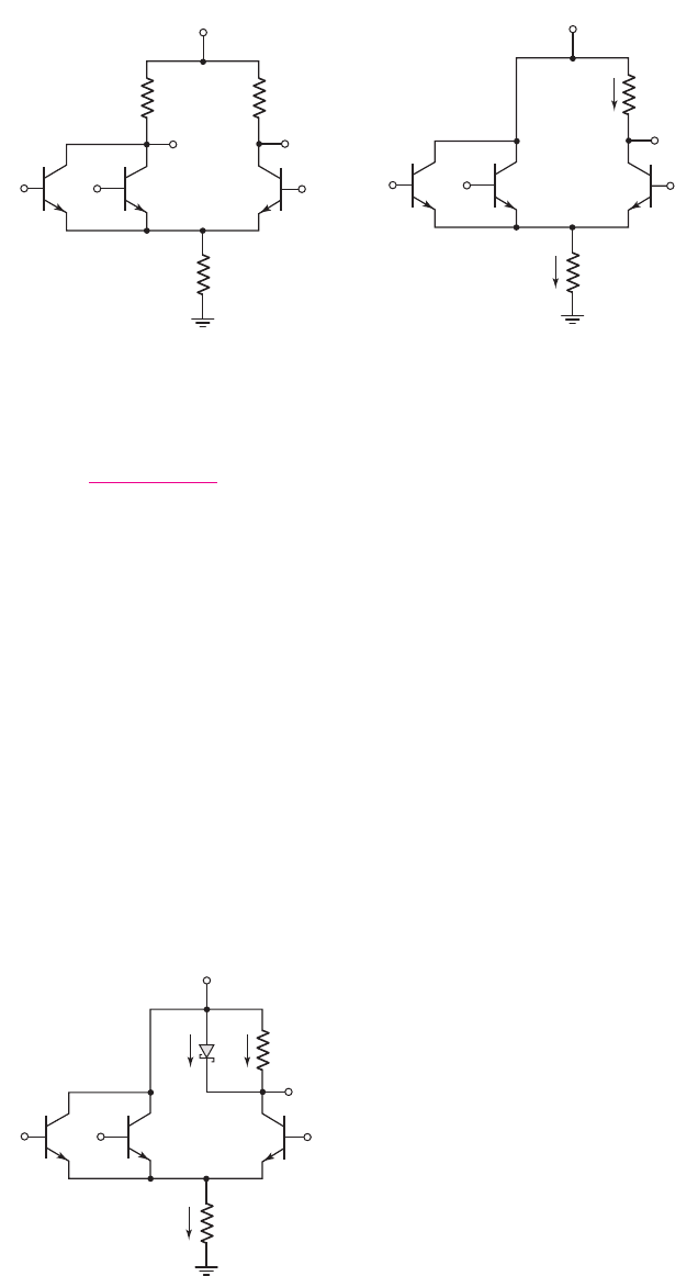
Figure 17.9 (a) Basic ECL OR/NOR logic gate and (b) modified ECL logic gate
v
OR
v
Y
v
X
V
R
R
E
R
C
Q
1
Q
2
V
CC
Q
R
i
E
i
R
i
D
Figure 17.10 Modified ECL logic gate with Schottky diode
nea80644_ch17_1255-1314.qxd 8/6/09 11:12 AM Page 1268 pmath DATA-DISK:Desktop Folder:UDAYVEER/Neamen:

Chapter 17 Bipolar Digital Circuits 1269
biased by 0.2 V. When
Q
R
is conducting, its collector voltage is
V
CC
− V
γ
, which
means that the B–C junction is now forward-biased by 0.2 V and the transistor is biased
slightly in saturation. However, this slight saturation bias does not degrade the switch-
ing of
Q
R
, so the fast switching characteristics of the ECL circuit are retained.
EXAMPLE 17.7
Objective: Analyze the modified ECL logic gate.
Consider the circuit in Figure 17.10 with parameters
V
CC
= 1.7V
and
R
E
=
R
C
= 8k
. Assume the diode and transistor piecewise linear parameters are
V
γ
= 0.4V
and
V
BE
(on) = 0.7V
.
Solution: The output voltage values are
v
OR
= logic 1 = V
CC
= 1.7V
and
v
OR
= logic 0 = V
CC
− V
γ
= 1.7 −0.4 = 1.3V
For the output voltages to be compatible with the inputs, the reference voltage
V
R
must be the average of the logic 1 and logic 0 values, or
V
R
= 1.5V
. If
v
X
= v
Y
=
logic 0 = 1.3V
, then
Q
R
is on. Therefore,
i
E
=
V
R
− V
BE
(on)
R
E
=
1.5 − 0.7
8
⇒ 100 μA
The maximum current in
R
C
is
i
R
(max) =
V
γ
R
C
=
0.4
8
⇒ 50 μA
and the current through the diode is
i
D
= i
E
−i
R
(max) = 100 −50 = 50 μA
For
v
X
= v
Y
= logic 0
, the power dissipation is
P = i
E
V
CC
, or
P = i
E
V
CC
= (100)(1.7) = 170 μW
For
v
X
= v
Y
= logic 1 = 1.7V
, we have
i
E
=
v
X
− V
BE
(on)
R
E
=
1.7 − 0.7
8
⇒ 125 μA
Therefore, the power dissipation for this condition is
P = i
E
V
CC
= (125)(1.7) = 213 μW
Comment: If the resistance values of
R
E
and
R
C
were to change by as much as
±20
percent as a result of manufacturing tolerances, for example, the currents would
still be sufficient to turn the Schottky diode on when
Q
R
is on. This means that the
logic 0 output is well defined. Also, the power dissipation in this ECL gate is consid-
erably less than that in the classic ECL OR/NOR logic circuit. The reduced power is
a result of fewer components, lower bias voltage, and smaller currents.
EXERCISE PROBLEM
Ex 17.7: Design the basic ECL logic gate in Figure 17.11 such that the maximum
power dissipation is 0.2 mW and the logic swing is 0.4 V. (Ans.
I
Q
= 117.6 μA
,
R
C
= 3.4k
,
V
R
= 1.5V
)
nea80644_ch17_1255-1314.qxd 8/6/09 11:12 AM Page 1269 pmath DATA-DISK:Desktop Folder:UDAYVEER/Neamen:
1270 Part 3 Digital Electronics
v
O
v
Y
v
X
V
R
R
C
V
CC
= 1.7 V
Q
1
Q
2
Q
R
I
Q
Figure 17.11 Figure for Exercise Ex 17.7
V
R
=
1.5 V
V
R
=
1.5 V
V
R
=
1.5 V
R
E
V
CC
= 1.7 V
V
CC
= 1.7 V
V
CC
= 1.7 V
v
Y
v
X
R
E
Q
1
Q
2
Q
R
R
E
Q
2
″
Q
2
′
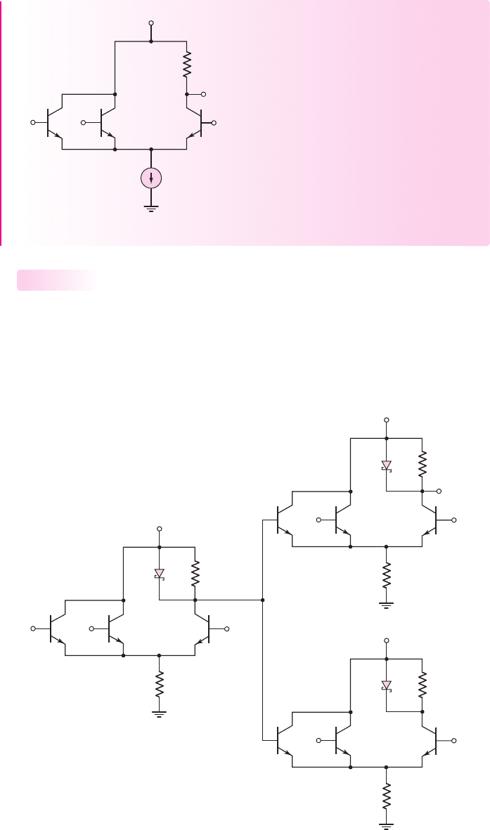
Figure 17.12 Modified ECL logic gate with two load circuits
Alternative ECL Gates
In an ECL system, as in all digital systems, a gate is used to drive other logic gates.
Connecting load circuits to the basic ECL gate demonstrates changes that can be
made to incorporate ECL into integrated circuits more effectively.
Figure 17.12 shows the basic ECL gate with two load circuits. In this config-
uration, the collectors of
Q
2
and
Q
2
are at the same potential, as are the bases of
17.2.2
nea80644_ch17_1255-1314.qxd 8/6/09 11:12 AM Page 1270 pmath DATA-DISK:Desktop Folder:UDAYVEER/Neamen:
Chapter 17 Bipolar Digital Circuits 1271
the two transistors. We can therefore replace
Q
2
and
Q
2
by a single multiemitter
transistor.
In Figure 17.13, the multiemitter transistor
Q
O
is part of the driver circuit. The
operation of the circuit is as follows:
•
v
x
= v
y
= logic 1 = 1.7V
: The two input transistors
Q
1
and
Q
2
are on,
Q
R
is off, and
v
O
= 1.7V
. Since the base voltage of
Q
O
is higher than the base
voltages of
Q
R
and
Q
R
, then
Q
O
is conducting,
Q
R
and
Q
R
are off, and
v
E
= v
E
= 1.7 −0.7 = 1.0V
. The currents
i
E
and
i
E
flow through the emit-
ters of
Q
O
. The output voltages are
v
O
= v
O
= 1.7V
.
•
v
x
= v
y
= logic 0 = 1.3V
: For this case, the two input transistors
Q
1
and
Q
2
are off,
Q
R
is on, and
v
O
= 1.3V
. The output transistor
Q
O
is off and
both
Q
R
and
Q
R
are on. The output voltages are then
v
O
= v
O
= 1.3V
.
The two load circuits in Figure 17.13 each have only a single input, which limits
the circuit functionality. The versatility of the circuit can be further enhanced by
making the load transistor
Q
R
a multiemitter transistor. This is shown in Fig-
ure 17.14. For simplicity, we show only a single input transistor to each of the two
v
O
′
v
E
′
V
CC
= 1.7 V
V
R
= 1.5 V
Q
O
v
O
v
Y
v
X
V
R
= 1.5 V
R
E
Q
1
Q
2
V
CC
= 1.7 V
Q
R
R
E
v
O
″
V
CC
= 1.7 V
V
R
= 1.5 V
v
E
″
R
E
i
E
″
Q
R
″
Q
R
′
i
E
′
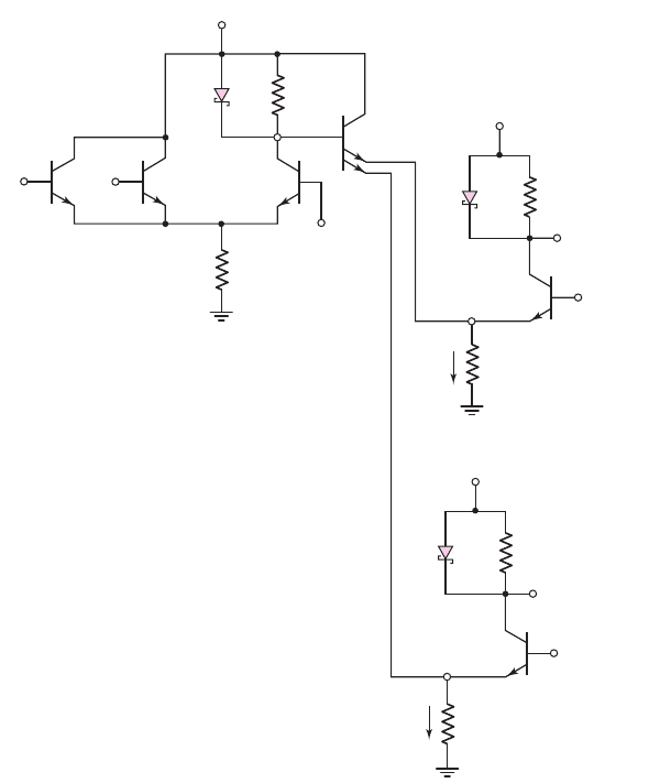
Figure 17.13 Modified ECL logic gate with multiemitter output transistor and two load circuits
nea80644_ch17_1255-1314.qxd 8/6/09 11:12 AM Page 1271 pmath DATA-DISK:Desktop Folder:UDAYVEER/Neamen:
1272 Part 3 Digital Electronics
driver circuits. The operation of this circuit for various combinations of input volt-
ages is as follows.
•
v
1
= v
2
= logic 0 = 1.3V
: The two input transistors
Q
1
and
Q
2
are off and
the two reference transistors
Q
R1
and
Q
R2
are on. This means that
v
O1
= v
O2
= 1.3V
and both output transistors
Q
O1
and
Q
O2
are off. Both
emitters of
Q
R
are forward biased, currents
i
E1
and
i
E2
flow through
Q
R
, and
the output voltage is
v
O
= logic 0 = 1.3V
.
•
v
1
= 1.7V
,
v
2
= 1.3V
: For this case,
Q
1
is on,
Q
R1
is off,
Q
2
is off, and
Q
R2
is on. The output voltages are
v
O1
= 1.7V
and
v
O2
= 1.3V
. This means that
Q
O1
is on and
Q
O2
is off. With
Q
O1
on, current
i
E1
flows through
Q
O1
and
no current flows in emitter
E
1
. With
Q
O2
off, emitter
E
2
is forward biased,
current
i
E2
flows through
Q
R
, and the output voltage is
v
O
= logic 0 = 1.3V
.
•
v
1
= 1.3V
,
v
2
= 1.7V
: This case is the complement of the one just dis-
cussed. Here,
Q
O1
is off and
Q
O2
is on. This means that
i
E1
flows through
emitter
E
1
of
Q
R
, and
i
E2
flows through
Q
O2
. The output voltage is
v
O
= logic 0 = 1.3V
.
•
v
1
= v
2
= 1.7V
: The two input transistors
Q
1
and
Q
2
are on, the two refer-
ence transistors
Q
R1
and
Q
R2
are off, and
v
O1
= v
O2
= 1.7V
. This means that
both
Q
O1
and
Q
O2
are on and
Q
R
is off. Currents
i
E1
and
i
E2
flow through
Q
O1
and
Q
O2
, respectively, and the output voltage is
v
O
= logic 1 = 1.7V
.
V
R
=
1.5 V
V
CC
= 1.7 V
v
1
v
O1
v
O
′
v
O2
E
2
V
CC
= 1.7 V
R
E
V
R
= 1.5 V
Q
1
Q
R1
V
R
=
1.5 V
V
CC
= 1.7 V
v
2
R
E
Q
2
Q
R2
R
E
R
E
i
E1
i
E2
Q
O2
Q
O1
Q
R
′
E
1
Figure 17.14 Two ECL driver circuits with a multi-input load circuit
nea80644_ch17_1255-1314.qxd 8/6/09 11:12 AM Page 1272 pmath DATA-DISK:Desktop Folder:UDAYVEER/Neamen:
Chapter 17 Bipolar Digital Circuits 1273
These results are summarized in Table 17.1, which shows that this circuit
performs the AND logic function. A more complicated or sophisticated logic func-
tion can be performed if multiple inputs are used in the driver circuits.
In integrated circuits, resistors R
E
are replaced by current sources using transis-
tors. Replacing resistors with transistors in integrated circuits usually results in
reduced chip area.
Series Gating
Series gating is a bipolar logic circuit technique that allows complex logic functions
to be performed with a minimum number of devices and with maximum speed.
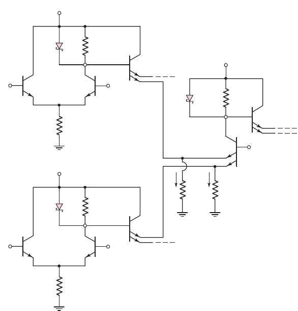
Series gating is formed by using cascode stages.
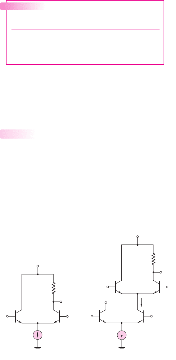
Figure 17.15(a) shows the basic emitter-coupled pair, and Figure 17.15(b) shows
a cascode stage, also referred to as two-level series gating. Reference voltage
V
R1
is
approximately 0.7 V greater than reference voltage
V
R2
. The input voltages
v
x
and
v
y
must also be shifted approximately 0.7 V with respect to each other.
As an example, we use the multiemitter load circuit from Figure 17.14 as part of
a cascode configuration as shown in Figure 17.16. Transistors
Q
O1
,
Q
O2
, and
Q
O3
17.2.3
Table 17.1 Summary of results for the ECL circuit in
Figure 17.14
v
1
(V) v
2
(V) v
O
(V)
1.3 1.3 1.3
1.7 1.3 1.3
1.3 1.7 1.3
1.7 1.7 1.7
v
O
V
R
v
X
I
Q
R
L
V
CC
v
O
V
R1
v
X
R
L
V
CC
V
CC
V
R2
v
Y
I
Q
i
O
(a) (b)
Figure 17.15 (a) Basic emitter-coupled pair and (b) ECL cascode configuration
nea80644_ch17_1255-1314.qxd 8/6/09 11:12 AM Page 1273 pmath DATA-DISK:Desktop Folder:UDAYVEER/Neamen:
represent the output transistors of three ECL driver circuits. We assume a logic 1 level
of 2.5 V and a logic 0 level of 2.1 V. The 0.4 V logic swing results from incorporat-
ing a Schottky diode in each output stage.
With three input signals, there are eight possible combinations of input states.
We will only consider two combinations here:
•
A = B = C = logic 0 = 2.1V
: In this case, transistors
Q
O1
and
Q
O2
are off
and transistor
Q
1
is off. This means that current
I
Q
flows through
Q
2
and
Q
R
, and
v
O
= logic 0 = 2.1V
.
•
A = C = 2.1V
,
B = 2.5V
: Transistors
Q
O1
and
Q
1
are off,
Q
O2
is on, and
current
I
Q
flows through
Q
2
and
Q
O2
. Since
Q
1
is off, no current is available to
flow through
Q
R
, even though
Q
O1
is off. The output is
v
O
=logic 1 = 2.5V
.
For the output voltage
v
O
to be a logic 1, no current must flow through
Q
R
. This
occurs when both
Q
O1
and
Q
O2
are on, or when a B–E junction of
Q
R
is turned on
but no current is available through
Q
1
or
Q
2
. We can show that this circuit performs
the logic of function
(A AND C) OR (B AND
¯
C)
(17.8)
We are now beginning to integrate logic functions into a circuit rather than using
separate, distinct logic gates. This reduces the number of devices required, as well as
the propagation delay time.
Another example of series gating is shown in Figure 17.17. A negative supply
voltage is again used. The operation of the circuit is as follows.
•
v
x
= v
y
= logic 0 =−0.4V
: Transistors
Q
1
,
Q
4
, and
Q
7
are on, current
I
Q
flows through
Q
7
and
Q
4
, the diode turns on, and the output voltage is
−0.4V
.
•
v
x
=−0.4V
,
v
y
= 0
: Transistors
Q
1
,
Q
4
, and
Q
6
are on, current
I
Q
flows
through
Q
6
and
Q
1
to ground, and current
I
Q2
flows through
Q
4
and the
1274 Part 3 Digital Electronics
v
O
V
CC
= 2.5 V
V
R2
= 1.6 V
I
Q
V
CC
= 2.5 V
V
CC
= 2.5 V
V
CC
= 2.5 V
V
R1
= 2.3 V
Q
R
Q
O3
Q
O2
Q
2
Q
1
Q
O1
A
B
C
Q
O
Figure 17.16 ECL series gating example
nea80644_ch17_1255-1314.qxd 8/6/09 11:12 AM Page 1274 pmath DATA-DISK:Desktop Folder:UDAYVEER/Neamen:
Chapter 17 Bipolar Digital Circuits 1275
resistor. The output voltage is
v
O
=−R
C
I
Q2
=−(1)(0.05) =−0.05 V
.
This voltage is not sufficient to turn the Schottky diode on. Although it is not
zero volts, the voltage still represents a logic 1.
•
v
x
= 0
,
v
y
=−0.4
V: Transistors Q
2
,Q
3
, and Q
7
are on, current I
Q
flows
through Q
7
and Q
3
to ground, and current I
Q1
flows through Q
2
and the
resistor. Again,
v
O
=−0.05
V
=
logic 1.
•
v
x
= v
y
= logic 1
∼
=
0V
: Transistors
Q
2
,
Q
3
, and
Q
6
are on,
I
Q
flows
through
Q
6
,
Q
2
, and the Schottky diode, and output voltage is
v
O
=
−0.4V= logic 0
.
These results are summarized in Table 17.2, in which the logic levels are given.
The results show that the circuit performs the exclusive-OR logic function.
Propagation Delay Time
ECL is the fastest bipolar logic technology. Bipolar technology can produce small,
very fast transistors with cutoff frequencies in the range of 3 to 15 GHz. Logic gates
that use these transistors are so fast that interconnect line delays tend to dominate the
propagation delay times. Minimizing these interconnect delays involves minimizing
the metal lengths and using sufficient current drive capability.
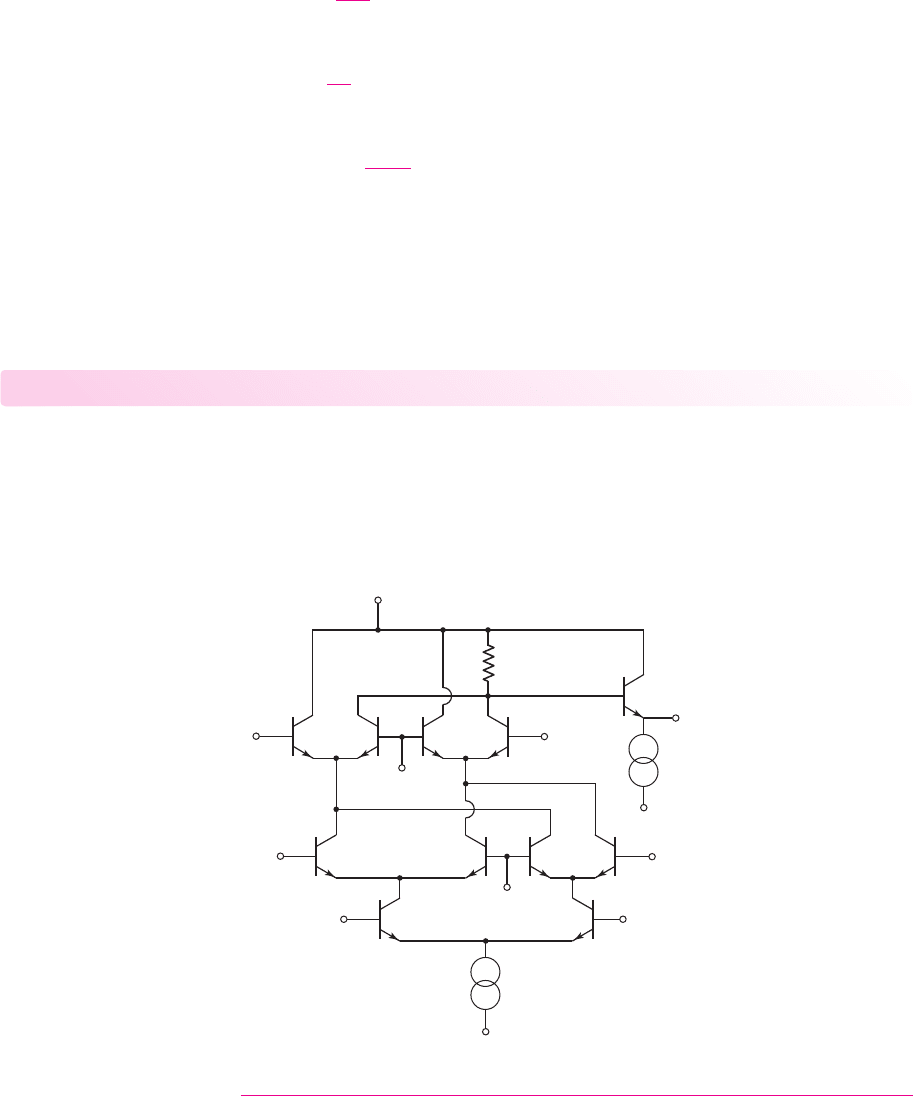
Speed is derived from low-signal logic swings, nonsaturating logic, and the abil-
ity to drive a load capacitance. Figure 17.18 is the emitter-follower output stage
17.2.4
v
O
v
X
v
Y
Q
7
Q
6
Q
2
Q
3
Q
4
Q
1
I
Q
= 500 m A
Q
5
–3 V
–3 V
–0.9 V
–3 V
–3 V
–
0.2 V
–0.2 V
1 kΩ
250 mA
I
Q1
= 50 mA
I
Q2
= 50 mA
Figure 17.17 ECL series gating example
Table 17.2 Summary of logic levels for
ECL circuit in Figure 17.17
v
x
v
y
v
O
000
011
101
110
V
EE
I
Q
C
L
v
O
v
I
Figure 17.18 Emitter-
follower stage with load
capacitance
nea80644_ch17_1255-1314.qxd 8/6/09 11:12 AM Page 1275 pmath DATA-DISK:Desktop Folder:UDAYVEER/Neamen:
1276 Part 3 Digital Electronics
found in many ECL circuits, showing an effective load capacitance. Usually, the
emitter-follower current
I
Q
is two to four times larger than the cell current.
In the pull-down cycle, the current
I
Q
discharges
C
L
. The current–voltage rela-
tionship of the capacitor is
i = C
L
dv
O
dt
(17.9(a))
or
v
O
=
1
C
L
idt
(17.9(b))
Assuming
C
L
and
i = I
Q
are constants, the fall time is
τ
F
= (0.8)
C
L
V
S
I
Q
(17.10)
where
V
S
is the logic swing, and the factor (0.8) occurs because
τ
F
is defined as the
time required for the output to swing from 10 percent to 90 percent of its final value.
As an example, if
V
S
= 0.4V
and
I
Q
= 250 μA
, then for a minimum fall time
of
τ
F
= 0.8ns
, the maximum load capacitance is
C
L
(max) = 0.625 pF
. This calcu-
lation shows that the load capacitance must be minimized to realize short propaga-
tion delay times.
Test Your Understanding
TYU 17.3 Consider the ECL circuit in Figure 17.16. For each of the eight possible
combinations of input states, determine the conduction state (on or off) of each tran-
sistor. Verify that this circuit performs the logic function given by Equation (17.8).
TYU 17.4 The ECL circuit in Figure 17.19 is an example of three-level series gating.
Determine the logic function that the circuit performs. (Ans.
(A ⊕ B) ⊕C
)
R
L
v
O
V
CC
V
EE
I
S
= 300 mA
I
T
= 75 mA
V
EE
V
R1
A
A
B
B
C
V
R2
V
R3
Figure 17.19 Figure for Exercise TYU 17.4
nea80644_ch17_1255-1314.qxd 8/6/09 11:12 AM Page 1276 pmath DATA-DISK:Desktop Folder:UDAYVEER/Neamen:
Chapter 17 Bipolar Digital Circuits 1277
17.3 TRANSISTOR–TRANSISTOR LOGIC
Objective: • Analyze transistor–transistor logic circuits
The bipolar inverter is the basic circuit from which most bipolar saturated logic cir-
cuits are developed, including diode–transistor logic (DTL) and transistor–transistor
logic (TTL). However, the basic bipolar inverter suffers from loading effects.
Diode–transistor logic combines diode logic (Chapter 2) and the bipolar inverter to
minimize loading effects. Transistor–transistor logic, which evolved directly from
DTL, provides reduced propagation delay times, as we will show.
In DTL and TTL circuits, bipolar transistors are driven between cutoff and satu-
ration. Since the transistor is being used essentially as a switch, the current gain is not
as important as in amplifier circuits. Typically, for transistors used in these circuits,
the current gain is assumed to be in the range of 25 to 50. These transistors need not
be fabricated to as tight a tolerance as that of high-gain amplifier transistors.
Table 17.3 lists the piecewise linear parameters used in the analysis of bipolar
digital circuits, along with their typical values. Also included is the pn junction diode
turn-on voltage
V
γ
. Generally, the B–E voltage increases as the transistor is driven
into saturation, since the base current increases. When the transistor is biased in the
saturation region, the B–E voltage is
V
BE
(sat)
, where
V
BE
(sat)>V
BE
(on)
.
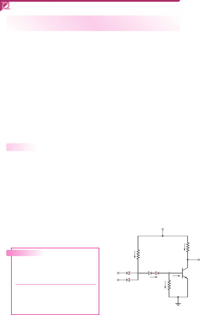
Basic Diode–Transistor Logic Gate
The basic diode–transistor logic (DTL) gate is shown in Figure 17.20. The circuit is
designed such that the output transistor operates between cutoff and saturation. This
provides the maximum output voltage swing, minimizes loading effects, and pro-
duces the maximum noise margins. When
Q
o
is in saturation, the output voltage is
v
O
= V
CE
(sat)
∼
=
0.1V
and is defined as logic 0 for the DTL circuit. As we will see,
the basic DTL logic gate shown in Figure 17.20 performs the NAND logic function.
Basic DTL NAND Circuit Operation
If both input signals
v
X
and
v
Y
are at logic 0, then the two input diodes
D
X
and
D
Y
are forward biased through resistor
R
1
and voltage source
V
CC
. The input diodes
17.3.1
Table 17.3 Piecewise linear
parameters for a pn
junction diode and
npn bipolar transistor
Parameter Value
V
γ
0.7 V
V
BE
(on) 0.7 V
V
BE
(sat) 0.8 V
V
CE
(sat) 0.1 V
v
X
D
X
D
Y
v
Y
V
CC
= 5 V
v
O
v
1
R
C
= 4 kΩ
R
B
=
10 kΩ
Q
o
R
1
= 4 kΩ
i
2
D
2
i
B
i
R
i
RC
i
1
D
1
v
B
Figure 17.20 Basic diode–transistor logic gate
nea80644_ch17_1255-1314.qxd 8/6/09 11:12 AM Page 1277 pmath DATA-DISK:Desktop Folder:UDAYVEER/Neamen: