Neamen D. Microelectronics: Circuit Analysis and Design
Подождите немного. Документ загружается.


1278 Part 3 Digital Electronics
conduct, and voltage
v
1
is clamped to a value that is one diode drop above the input
voltage. If
v
X
= v
Y
= 0.1V
and
V
γ
= 0.7V
, then
v
1
= 0.8V
. Diodes
D
1
and
D
2
and output transistor
Q
o
are nonconducting and are off. If
D
1
and
D
2
were conduct-
ing, then voltage
v
B
would be
−0.6V
for
V
γ
= 0.7V
. However, no mechanism
exists for
v
B
to become negative and still have a forward-biased diode current. Thus,
the current in
D
1
and
D
2
, the current in
Q
o
, and the voltage
v
B
are all zero. Since
Q
o
is cut off, then the output voltage is
v
O
= V
CC
. This is the largest possible output
voltage and is therefore defined as the logic 1 level. This same condition applies as
long as at least one input is at logic 0.
When both
v
X
and
v
Y
are at logic 1, which is equal to
V
CC
, both
D
X
and
D
Y
are
cut off. Diodes
D
1
and
D
2
become forward biased, output transistor
Q
o
is driven into
saturation, and
v
O
= V
CE
(sat)
, which is the smallest possible output voltage and is
defined as the logic 0 level.
This circuit is a two-input DTL NAND logic gate. However, the circuit is not
limited to two inputs. Additional input diodes may be included to increase the fan-in.
EXAMPLE 17.8
Objective: Determine the currents and voltages in the DTL logic circuit.
Consider the DTL circuit in Figure 17.20. Assume the transistor parameters are
as given in Table 17.3 and let
β = 25
.
Solution: Let
v
X
= v
Y
= logic 0 = 0.1V
. For this case,
v
1
= v
X
+ V
γ
= 0.1 +0.7 = 0.8V
and
i
1
=
V
CC
−v
1
R
1
=
5 − 0.8
4
= 1.05 mA
Since diodes
D
1
and
D
2
and output transistor
Q
o
are nonconducting, we assume that
current
i
1
divides evenly between the matched diodes
D
X
and
D
Y
. In this case, the
currents
i
2
= i
B
= i
C
= 0
and the output voltage is
v
O
= 5V= logic 1
.
If
v
X
= 0.1V
and
v
Y
= 5V
, or
v
X
= 5V
and
v
Y
= 0.1V
, then the output tran-
sistor is still cut off and
v
O
= 5V= logic 1
.
If
v
X
= v
Y
= logic 1 = 5V
, it is impossible for input diodes
D
X
and
D
Y
to be
forward biased. In this case, diodes
D
1
and
D
2
and the output transistor are biased
on, which means that, starting at ground potential at the emitter of
Q
o
,
v
1
is
v
1
= V
BE
(sat) + 2V
γ
= 0.8 +2(0.7) = 2.2V
Voltage
v
1
is clamped at this value and cannot increase. We see that
D
X
and
D
Y
are
indeed reverse biased and turned off, as assumed.
Currents
i
1
and
i
2
are
i
1
= i
2
=
V
CC
−v
1
R
1
=
5 − 2.2
4
= 0.70 mA
and current
i
R
is
i
R
=
V
BE
(sat)
R
B
=
0.8
10
= 0.08 mA
The base current into the output transistor is then
i
B
= i
2
−i
R
= 0.70 −0.08 = 0.62 mA
nea80644_ch17_1255-1314.qxd 8/6/09 11:12 AM Page 1278 pmath DATA-DISK:Desktop Folder:UDAYVEER/Neamen:

Chapter 17 Bipolar Digital Circuits 1279
Since the circuit is to be designed such that
Q
o
is driven into saturation, the collector
current is
i
C
=
V
CC
− V
CE
(sat)
R
C
=
5 − 0.1
4
= 1.23 mA
Finally, the ratio of collector to base current is
i
C
i
B
=
1.23
0.62
= 1.98 <β
Comment: Since the ratio of the collector current to base current is less than
β
, the
output transistor is biased in the saturation region. Since the output transistor is biased
between cutoff and saturation, the maximum swing between logic 0 and logic 1 is
obtained.
EXERCISE PROBLEM
Ex 17.8: Consider the basic DTL circuit in Figure 17.20 with circuit and transis-
tor parameters given in Example 17.8. Assume no load is connected to the output.
Calculate the power dissipated in the circuit for (a)
v
X
= v
Y
= 5V
and (b)
v
X
=
v
Y
= 0
. (Ans. (a)
P = 9.625
mW, (b)
P = 5.375
mW)
Minimum β
To ensure that the output transistor is in saturation, the common-emitter current gain
β
must be at least as large as the ratio of collector current to base current. For exam-
ple 17.8, the minimum
β
, or
β
min
, is 1.98. If the common-emitter current gain were
less than 1.98, then
Q
o
would not be driven into saturation, and the currents and volt-
ages in the circuit would have to be recalculated. A current gain greater than 1.98
ensures that
Q
o
is driven into saturation for the given circuit parameters and for the
no-load condition.
Pull-Down Resistor
In the basic DTL NAND logic circuit in Figure 17.20, a resistor
R
B
is connected
between the base of the output transistor and ground. This resistor is called a pull-
down resistor, and its purpose is to decrease the output transistor switching time as it
goes from saturation to cutoff. As previously discussed, excess minority carriers
must be removed from the base before a transistor can be switched to cutoff. This
base charge removal produces a current out of the transistor base terminal until the
transistor is turned off. Without the pull-down resistor, this reverse base current
would be limited to the reverse-bias leakage current in diodes
D
1
and
D
2
, resulting
in a relatively long turn-off time. The pull-down resistor provides a path for the
reverse base current.
The base charge can be removed more rapidly if the value of
R
B
is reduced. The
larger the reverse base current, the shorter the transistor turn-off time. However, a
trade-off must be made in choosing the value of
R
B
. A small
R
B
provides faster
switching, but lowers the base current to the transistor in the on state by diverting
some drive current to ground. A lower base current reduces the circuit drive capability,
or maximum fanout.
nea80644_ch17_1255-1314.qxd 8/6/09 11:12 AM Page 1279 pmath DATA-DISK:Desktop Folder:UDAYVEER/Neamen:
1280 Part 3 Digital Electronics
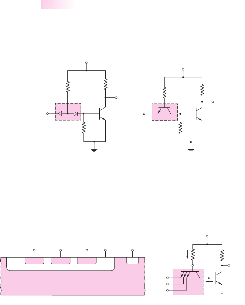
(a) (b)
v
X
V
CC
v
O
R
C
R
1
R
B
Q
o
Q
1
v
X
D
X
V
CC
v
O
R
C
R
1
R
B
Q
o
D
1
Figure 17.21 (a) Basic DTL gate and (b) basic TTL gate
(a) (b)
p
n
E
1
E
2
E
3
BC
v
O
Q
o
Q
1
v
B1
v
C1
v
X
v
Y
v
Z
R
C
= 4 kΩ
R
1
= 4 kΩ
V
CC
= 5 V
i
B1
E
2
E
1
E
3
i
C1
n
+
n
+
n
+
n
+
Figure 17.22 (a) Simplified cross section of three-emitter transistor and (b) TTL circuit with
three-emitter input transistor
The Input Transistor of TTL
Figure 17.21(a) shows a basic DTL circuit with one input diode
D
X
and one offset
diode
D
1
. The structure of these back-to-back diodes is the same as an npn transistor,
as indicated in Figure 17.21(b). The base–emitter junction of
Q
1
corresponds to
input diode
D
X
and the base–collector junction corresponds to offset diode
D
1
.
17.3.2
In isoplanar integrated circuit technology, the emitter of a bipolar transistor is
fabricated in the base region. More emitters can then be added in the same base region
to form a multiemitter, multi-input device. Figure 17.22(a) shows a simplified cross
section of a three-emitter transistor, which is used as the input device in a TTL circuit.
Figure 17.22(b) shows the basic TTL circuit with the multiemitter input transistor.
This circuit performs the same NAND operation as its DTL counterpart. The
multiemitter transistor reduces the silicon area required, compared to the DTL input
diodes, and it increases the switching speed. Transistor
Q
1
assists in pulling output
transistor
Q
o
out of saturation and into cutoff during a low-to-high transition of the
nea80644_ch17_1255-1314.qxd 8/6/09 11:12 AM Page 1280 pmath DATA-DISK:Desktop Folder:UDAYVEER/Neamen:
Chapter 17 Bipolar Digital Circuits 1281
output voltage. Pull-down resistor
R
B
in Figure 17.21(b) is no longer necessary, since
the excess minority carriers in the base of
Q
o
use transistor
Q
1
as a path to ground.
The operation of input transistor
Q
1
is somewhat unconventional. In Fig-
ure 17.23(a), if either or both of the two inputs to
Q
1
are in a low state, the
base–emitter junction is forward biased through
R
1
and
V
CC
. The base current enters
Q
1
, and the emitter current exits the specific emitter connected to the low input.
Transistor action forces the collector current into
Q
1
, but the only steady-state col-
lector current in this direction is a reverse-bias saturation current out of the base of
Q
o
. The steady-state collector current of
Q
1
is usually much smaller than the base
current, implying that
Q
1
is biased in saturation.
If at least one input is low such that
Q
1
is biased in saturation, then from Fig-
ure 17.23(a), we see that the base voltage of
Q
1
is
v
B1
= v
X
+ V
BE
(sat)
(17.11)
and the base current into
Q
1
is
i
B1
=
V
CC
−v
B1
R
1
(17.12)
If the forward current gain of
Q
1
is
β
F
, then
Q
1
will be in saturation as long as
i
C1
<β
F
i
B1
.
The collector voltage of
Q
1
is
v
C1
= v
X
+ V
CE
(sat)
(17.13)
If both
v
X
and
V
CE
(sat)
are approximately 0.1 V, then
v
C1
is small enough for the
output transistor to cut off and
v
O
= V
CC
= logic 1
.
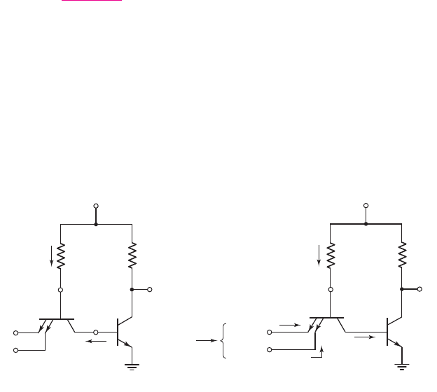
(a) (b)
v
B1
v
O
v
X
= 5 V
v
Y
= 5 V
V
CC
= 5 V
R
C
=
4 kΩ
i
B1
i
C1
i
EX
i
EY
i
ER
Q
o
Q
1
R
1
= 4 kΩ
v
B1
v
C1
v
O
v
X
v
Y
V
CC
= 5 V
R
C
=
4 kΩ
i
B1
i
C1
Q
o
Q
1
R
1
= 4 kΩ
Figure 17.23 TTL circuit (a) with at least one input low and (b) with all inputs high
If all inputs are high,
v
X
= v
Y
= 5V
, as shown in Figure 17.23(b), then the
base–emitter junctions of the input transistor are reverse biased. Base voltage
v
B1
increases, which forward-biases the B–C junction of
Q
1
and drives output transistor
Q
o
into saturation. Since the B–E junction of
Q
1
is reverse biased and the B–C junc-
tion is forward biased,
Q
1
is biased in the inverse-active mode. In this bias mode, the
roles of the emitter and collector are interchanged.
nea80644_ch17_1255-1314.qxd 8/6/09 11:12 AM Page 1281 pmath DATA-DISK:Desktop Folder:UDAYVEER/Neamen:

1282 Part 3 Digital Electronics
When input transistor
Q
1
is biased in the inverse-active mode, base voltage
v
B1
is
v
B1
= V
BE
(sat)
Q
o
+ V
BC
(on)
Q
1
(17.14)
where
V
BC
(on)
is the B–C junction turn-on voltage. We assume that the B–C junc-
tion turn-on voltage is equal to the B–E junction turn-on voltage. The terminal
current relationships for
Q
1
are therefore
i
EX
= i
EY
= β
R
i
B1
(17.15)
and
i
C1
= i
B1
+i
EX
+i
EY
= (1 +2β
R
)i
B1
(17.16)
where
β
R
is the inverse-active mode current gain of each input emitter of the input
transistor.
Since a bipolar transistor is not symmetrical, the inverse and forward current
gains are not equal. The inverse current gain is generally quite small, usually less
than one. In Figure 17.23(b), the input transistor has a fan-in of two. Transistor
Q
1
may be considered as two separate transistors with their bases and collectors con-
nected. For simplicity, when all inputs are high, we assume that current
i
ER
splits
evenly between the input emitters.
The inverse-active mode current into the emitters of
Q
1
is not desirable, since this
is a load current that must be supplied by a driver logic circuit when its output voltage
is in its high state. Because of the transistor action, these currents tend to be larger than
the reverse saturation currents of DTL circuit input diodes. The major advantage of
TTL over DTL is faster switching of the output transistor from saturation to cutoff.
If all inputs are initially high and then at least one input switches to the logic 0
state, 0.1 V, the B–E junction of
Q
1
becomes forward biased and base voltage
v
B1
becomes approximately
0.1 + 0.7 = 0.8V
. Collector voltage
v
C1
is held at 0.8 V as
long as output transistor
Q
o
remains in saturation. At this instant in time,
Q
1
is
biased in the forward-active mode. A large collector current into
Q
1
can exist, which
pulls the excess minority carrier charge out of the base of
Q
o
. A large reverse
base current from
Q
o
will very quickly pull the output transistor out of saturation. In
the TTL circuit, the action of the input transistor reduces the propagation delay time
compared to that of DTL logic circuits. For example, the propagation delay time is
reduced from approximately 40 ns in a DTL NAND gate to approximately 10 ns in
an equivalent TTL circuit.
Basic TTL NAND Circuit
We can improve the circuit performance of the simple TTL circuit in Figure 17.23 by
adding a second current gain stage. The resulting basic TTL NAND circuit is shown
in Figure 17.24. In this circuit, both transistors
Q
2
and
Q
o
are driven into saturation
when
v
X
= v
Y
= logic 1
. When at least one input switches from high to low, input
transistor
Q
1
very quickly pulls
Q
2
out of saturation and pull-down resistor
R
B
provides a path for the excess charge in
Q
o
, which means that the output transistor
can turn off fairly quickly.
DC Current–Voltage Analysis
The analysis of the TTL circuit is very similar to that of the DTL circuit, as demon-
strated in the following example.
17.3.3
nea80644_ch17_1255-1314.qxd 8/6/09 11:12 AM Page 1282 pmath DATA-DISK:Desktop Folder:UDAYVEER/Neamen:
Chapter 17 Bipolar Digital Circuits 1283
EXAMPLE 17.9
Objective: Calculate the currents and voltages for the basic TTL NAND circuit.
Consider the TTL circuit in Figure 17.24. Assume the piecewise linear transistor
parameters are as listed in Table 17.3. Assume the forward current gain is
β
F
≡ β = 25
and the inverse current gain of each input emitter is
β
R
= 0.1
.
Solution: For
v
X
= v
Y
= 0.1
V,
Q
1
is biased in saturation and
v
B2
= v
X
+v
CE
(sat) = 0.1 +0.1 = 0.2V
which means that
Q
2
and
Q
o
are both cut off. The base voltage
v
B1
is then
v
B1
= v
X
+v
BE
(sat) = 0.1 +0.8 = 0.9V
and current
i
1
is
i
1
=
V
CC
−v
B1
R
1
=
5 − 0.9
4
= 1.03 mA
This current flows out of the input transistor emitters. Since
Q
2
and
Q
o
are cut off,
all other currents are zero and the output voltage is
v
O
= 5V
.
If
v
X
= v
Y
= 5V
, then the input transistor is biased in the inverse active mode.
The base voltage
v
B1
is
v
B1
= V
BE
(sat)
Q
o
+ V
BE
(sat)
Q
2
+ V
BC
(on)
Q
1
= 0.8 +0.8 +0.7 = 2.3V
and the collector voltage
v
C2
is
v
C2
= V
BE
(sat)
Q
o
+ V
CE
(sat)
Q
2
= 0.8 +0.1 = 0.9V
The currents are
i
1
=
V
CC
−v
B1
R
1
=
5 − 2.3
4
= 0.675 mA
v
C2
v
Bo
v
X
v
Y
V
CC
= 5.0 V
v
O
v
B1
v
B2
R
C
= 4.0 kΩ
R
2
= 1.6 kΩ
R
B
=
1.0 kΩ
Q
2
Q
o
Q
1
R
1
=
4.0 kΩ
i
E2
i
Bo
i
B2
i
4
i
3
i
2
i
1
Figure 17.24 TTL circuit with currents and voltages
nea80644_ch17_1255-1314.qxd 8/6/09 11:12 AM Page 1283 pmath DATA-DISK:Desktop Folder:UDAYVEER/Neamen:

1284 Part 3 Digital Electronics
and
i
B2
= (1 +2β
R
)i
1
= (1 +0.2)(0.675) = 0.810 mA
Also,
i
2
=
V
CC
−v
C2
R
2
=
5 − 0.9
1.6
= 2.56 mA
which means that
i
E2
= i
2
+i
B2
= 2.56 +0.81 = 3.37 mA
The current in the pull-down resistor is
i
4
=
V
BE
(sat)
R
B
=
0.8
1
= 0.8mA
and the base drive to the output transistor is
i
Bo
= i
E2
−i
4
= 3.37 −0.8 = 2.57 mA
Current
i
3
is
i
3
=
V
CC
− V
CE
(sat)
R
C
=
5 − 0.1
4
= 1.23 mA
Comment: As mentioned, the analysis of the basic TTL circuit is essentially the
same as that of the DTL circuit. The magnitudes of currents and voltages in the basic
TTL circuit are also very similar to the DTL results.
EXERCISE PROBLEM
Ex 17.9: The parameters of the TTL NAND circuit in Figure 17.24 are:
R
1
= 12
k
,
R
2
= 4
k
,
R
B
= 2
k
, and
R
C
= 6
k
. Assume
β
F
≡ β = 25
and
β
R
= 0.1
(for each input emitter). For a no-load condition, determine the
base and collector currents in each transistor for: (a)
v
X
= v
Y
= 0.1
V and
(b)
v
X
= v
Y
= 5
V. (Ans. (a)
i
1
= i
B1
= 0.342
mA,
i
C1
∼
=
0
,
i
B2
= i
C2
= 0
,
i
Bo
= i
Co
= 0
; (b)
i
1
= i
B1
= 0.225
mA,
i
B2
=
|
i
C1
|
= 0.27
mA,
i
2
= i
C2
=
1.025
mA,
i
Bo
= 0.895
mA,
i
Co
= 0.8167
mA)
TTL Output Stages and Fanout
The propagation delay time can be improved by replacing the output collector resis-
tor with a current source.
When the output changes from low to high, the load capacitance must be
charged by a current through the collector pull-up resistor. The total load capacitance
is composed of the input capacitances of the load circuits and the capacitances of
the interconnect lines. The associated RC time constant for a load capacitance
of 15 pF and a collector resistance of
4k
is 60 ns, which is large compared to the
propagation delay time of a commercial TTL circuit.
Totem-Pole Output Stage
In Figure 17.25, the combination of
Q
3
,
D
1
, and
Q
o
forms an output stage called a
totem pole. Transistor
Q
2
forms a phase splitter, because the collector and emitter
voltages are 180 degrees out of phase. If
v
X
= v
Y
= logic 1
, input transistor
Q
1
is
17.3.4
nea80644_ch17_1255-1314.qxd 8/6/09 11:12 AM Page 1284 pmath DATA-DISK:Desktop Folder:UDAYVEER/Neamen:
Chapter 17 Bipolar Digital Circuits 1285
biased in the inverse-active mode, and both
Q
2
and
Q
o
are driven into saturation.
The voltage at the base of
Q
3
is
v
B3
= V
C2
= V
BE
(sat)
Q
o
+ V
CE
(sat)
Q
2
(17.17)
which is on the order of 0.9 V, and the output voltage is approximately 0.1 V. The
difference between the base voltage of
Q
3
and the output voltage is not sufficient to
turn
Q
3
and
D
1
on. The pn junction offset voltage associated with
D
1
must be included
so that
Q
3
is cut off when the output is low. For this condition, the saturation output
transistor discharges the load capacitance and pulls the output low very quickly.
If
v
X
= v
Y
= logic 0
, then
Q
2
and
Q
o
are cut off, and the base voltage to
Q
3
goes high. The transistor
Q
3
and diode
D
1
turn on so that the output load capacitance
can be charged and the output goes high. Since
Q
3
acts like an emitter follower, the
output resistance is small so that the effective RC time constant to charge the load
capacitance is now very small.
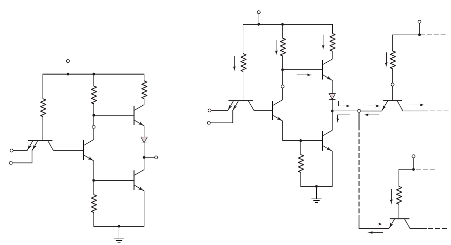
Fanout
Logic gates are not operated in isolation, but are used to drive other similar type logic
gates to implement a complex logic function. Figure 17.26 shows the TTL NAND
gate with a totem-pole output stage connected to N identical TTL NAND gates. The
maximum fanout is defined as the maximum number of similar-type logic circuits
that can be connected to the logic gate output without affecting proper circuit opera-
tion. For example, the output transistor
Q
o
must remain in saturation when the output
goes low to its logic 0 value. For a given value of
β
, there is then a maximum allow-
able load current, and therefore a maximum allowable number of load circuits that
can be connected to the output. As another condition, the output transistor is usually
rated for a maximum collector current. For an output low condition, the current
i
LL
is the load current that
Q
o
must sink from the load circuits.
v
B3
v
X
v
Y
+ 5 V
v
O
R
3
=
130 Ω
R
2
=
1.6 kΩ
R
B
=
1.0 kΩ
Q
2
Q
o
Q
3
D
1
Q
1
R
1
=
4.0 kΩ
Figure 17.25 TTL circuit with totem-pole
output stage
V
CC
= 5.0 V
V
CC
= 5.0 V
v
O
v
B3
R
3
= 130 Ω
R
2
=
1.6 kΩ
R
B
=
1.0 kΩ
Q
2
Q
3
Q
o
R
1
=
4.0 kΩ
R
1
N
= 4.0 kΩ
i
LL
i
L
′
H1
i
L
′
L1
i
L
′
HN
i
L
′
LN
i
N
′
i
LH
i
1
i
2
V
CC
= 5.0 V
v
B
′
1
Q
1
′
R
1
′
= 4.0 kΩ
i
B3
i
1
′
v
X
v
Y
D
1
Q
1
Q
1
N
′
Figure 17.26 TTL circuit with totem-pole output stage driving
N identical TTL stages
nea80644_ch17_1255-1314.qxd 8/6/09 11:12 AM Page 1285 pmath DATA-DISK:Desktop Folder:UDAYVEER/Neamen:

1286 Part 3 Digital Electronics
EXAMPLE 17.10
Objective: Calculate the maximum fanout for the output low condition.
Let
β = 25
for the output transistor.
Solution (Transistor Q
O
to remain in saturation): In Example 17.9, we calculated
the base current into
Q
o
as
i
Bo
= 2.57 mA
. The output voltage is
v
O
= 0.1V
so that
v
B1
= 0.1 +0.8 = 0.9
V. Each individual load current is then
i
LL1
= i
1
=
5 − 0.9
4
= 1.025 mA
The maximum collector current in
Q
o
is
i
Co
(max) = βi
Bo
= Ni
LL1
The maximum fanout, N, is then found as
N =
βi
Bo
i
LL1
=
(25)(2.57)
1.025
= 62.7
The number of load circuits must be an integer, so we round to the next lower integer,
or
N = 62
.
With 62 load circuits connected to the output, the collector current would be
i
Co
= Ni
LL1
= (62)(1.025) = 63.55 mA
which is a relatively large value. In most cases, the output transistor has a maximum
rated collector current that may limit the maximum fanout.
Solution (Maximum rated output current): If the maximum rated collector current
of the output transistor is
i
Co
(rated) = 20 mA
, then the maximum fanout is deter-
mined by
i
Co
(rated) = Ni
LL1
or
N =
i
Co
(rated)
i
LL1
=
20
1.025
= 19.5 → 19
Comment: In the first solution, the resulting fanout of 62 is not realistic since the
output transistor current is excessive. In the second solution, a maximum fanout of
19 is more realistic. However, another limitation in terms of proper circuit operation
is propagation delay time. For a large number of load circuits connected to the out-
put, the output load capacitance may be quite large which slows down the switching
speed to unacceptably large values. The maximum fanout, then, may be limited by
the propagation delay time specification.
EXERCISE PROBLEM
Ex 17.10: The TTL circuit shown in Figure 17.25 is redesigned such that
R
1
=
12
k
,
R
2
= 4
k
,
R
3
= 100
, and
R
B
= 2
k
. Assume that
β
F
≡ β = 25
and
β
R
= 0.1
(for each input emitter). Calculate the fanout for
v
X
= v
Y
= 3.6
V
under the condition that (a) the output transistor must remain in saturation and
(b) the maximum collector current of the output transistor is limited to 12 mA.
(Ans. (a)
N = 65
, (b)
N = 35
)
nea80644_ch17_1255-1314.qxd 8/6/09 11:12 AM Page 1286 pmath DATA-DISK:Desktop Folder:UDAYVEER/Neamen:
Chapter 17 Bipolar Digital Circuits 1287
Again, Figure 17.26 shows the TTL circuit with N identical load circuits and the
inputs in their low state. The input transistor is biased in saturation, and both
Q
2
and
Q
o
are cut off, causing base voltage
v
B3
and the output voltage to go high. The input
transistors of the load circuits are biased in the inverse-active mode, and the load
currents are supplied through
Q
3
and
D
1
. In this circuit, the input transistors of the
load gates are one-input NAND (inverter) gates, to illustrate the worst-case or maxi-
mum load current under the high input condition. Since the load current is supplied
through
Q
3
, a base current into
Q
3
must be supplied from
V
CC
through
R
2
. As the
load current increases, the base current through
R
2
increases, which means that volt-
age
v
B3
decreases because of the voltage drop across
R
2
. Assuming the B–E voltage
of
Q
3
and the diode voltage across
D
1
remain essentially constant, the output volt-
age
v
O
decreases from its maximum value.
A reasonable fanout of 10 or 15 for the high output condition means that the load
current will be small, base current
i
B3
will be very small, and the voltage drop across
R
2
will be negligible. The output voltage will then be approximately two diode drops
below
V
CC
. For typical TTL circuits, the
logic 1 = V
OH
value is on the order of
3.6 V, rather than the 5 V previously determined.
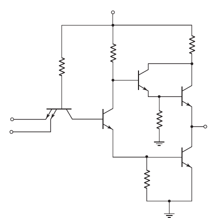
Modified Totem-Pole Output Stage
Figure 17.27 shows a modified totem-pole output stage in which transistor
Q
4
is used
in place of a diode. This has several advantages. First, the transistor pair
Q
3
and
Q
4
provides greater current gain, which in turn increases the fanout capability of this
circuit in its high state. Second, the output impedance in the high state is lower than
that of the single transistor, decreasing the switching time. Third, the base–emitter
junction of
Q
3
fulfills the function of diode
D
1
; therefore, the diode is no longer
needed to provide a voltage offset. In integrated circuits, the fabrication of transistors
is no more complex than the fabrication of diodes.
When the output is switched to its low state, resistor
R
4
provides a path to ground
for the minority carriers that must be pulled out of the base of
Q
3
to turn the transistor
v
X
v
Y
v
O
R
2
=
1.6 kΩ
V
CC
= 5.0 V
R
B
=
1.0 kΩ
Q
2
Q
3
Q
o
Q
4
Q
1
R
1
=
4.0 kΩ
R
3
=
130 Ω
R
4
=
4.0 kΩ
Figure 17.27 TTL circuit with modified totem-pole output stage
nea80644_ch17_1255-1314.qxd 8/6/09 11:12 AM Page 1287 pmath DATA-DISK:Desktop Folder:UDAYVEER/Neamen: