Neamen D. Microelectronics: Circuit Analysis and Design
Подождите немного. Документ загружается.

1298 Part 3 Digital Electronics
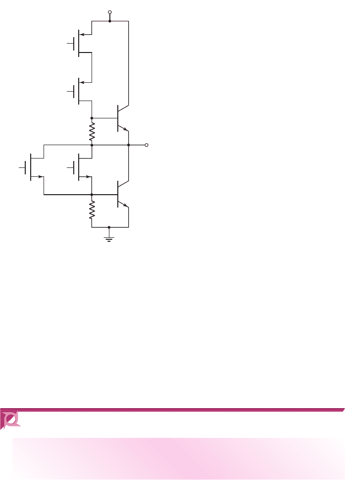
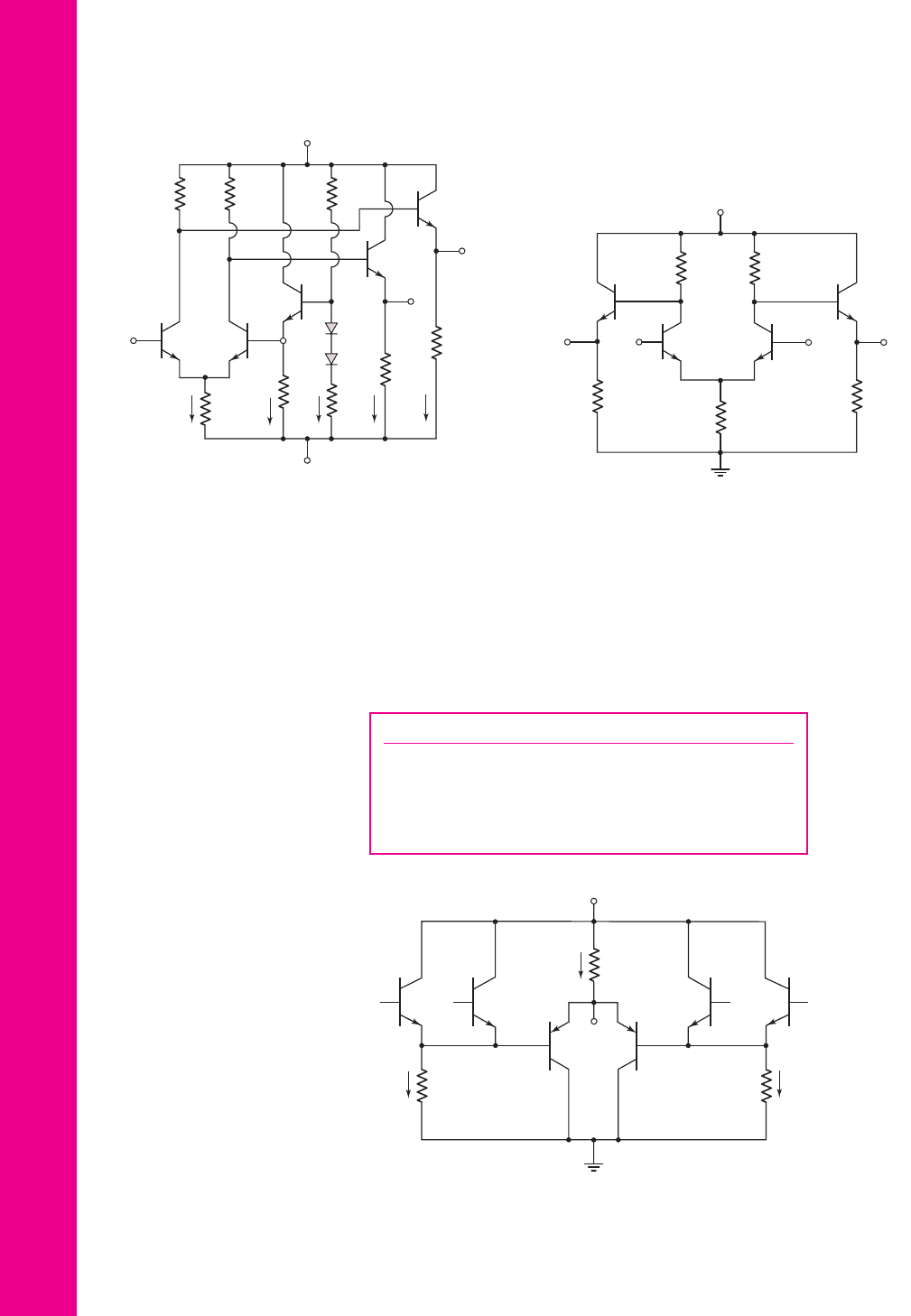
necessary current drive. One example of a BiCMOS logic circuit is shown in Figure
17.37. This is a two-input NOR gate. As seen in the figure, the CMOS configuration
is the same as the basic CMOS NOR logic gate considered previously. The two npn
output transistors and the
R
1
and
R
2
resistors have the same configuration and pur-
pose as was seen in the BiCMOS inverter.
Other BiCMOS logic circuits are designed in a manner similar to that shown for
the BiCMOS NOR gate.
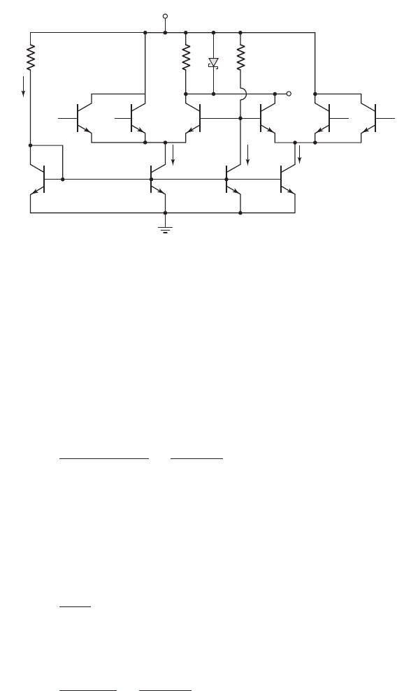
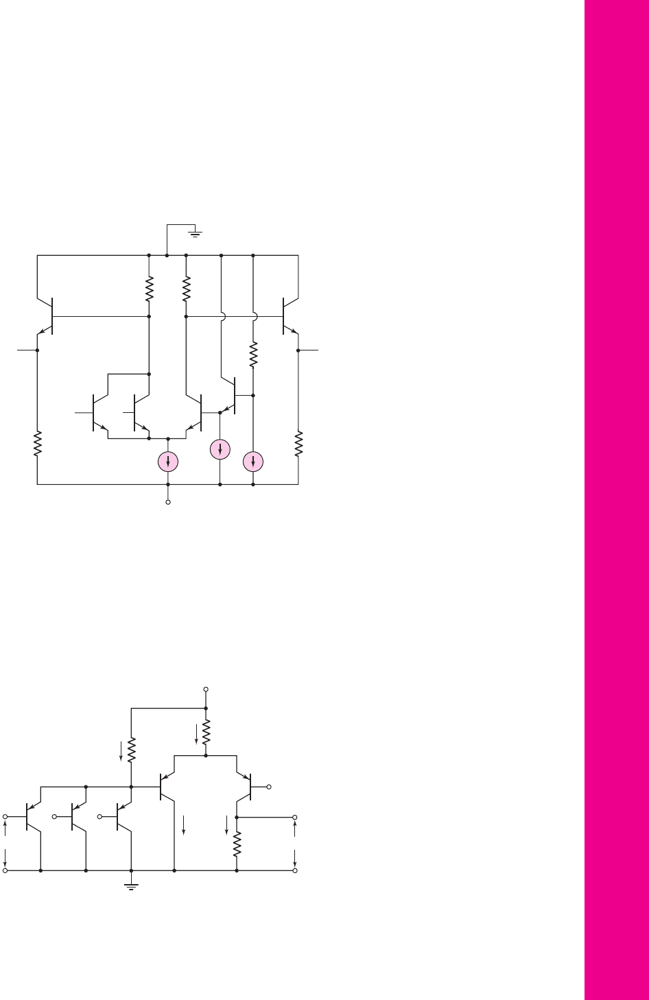
17.6 DESIGN APPLICATION: A STATIC ECL GATE
Objective: • Design a static ECL gate to implement a specific logic
function.
Specifications: A static ECL gate is to be designed to implement the logic function
Y = (A + B)(C + D)
. The circuit is to be designed using constant current sources
and the total power dissipation is to be no more than approximately 1 mw.
Design Approach: A modified static ECL gate with a Schottky diode similar to the
circuit configuration in Figure 17.10 is to be designed.
Choices: Inputs A, B, C, and D are assumed to be available. Simple two-transistor
current sources will be used.
V
DD
A
B
BA
v
O
Q
1
R
1
Q
2
R
2
Figure 17.37 Two-input BiCMOS NOR circuit
nea80644_ch17_1255-1314.qxd 8/6/09 11:12 AM Page 1298 pmath DATA-DISK:Desktop Folder:UDAYVEER/Neamen:
Chapter 17 Bipolar Digital Circuits 1299
I
Q
R
1
R
2
D
1
R
3
V
CC
= 1.7 V
V
O
V
R
I
REF
D C
Q
R1
AB
Q
R2
I
Q
I
Q
Figure 17.38 The static ECL gate for the design application
Solution (DC Circuit Design): There are four basic currents in the circuit. Assum-
ing that each bias current
I
Q
is equal to the reference current
I
REF
, then from the total
power dissipation, we find
P
T
= 1 = I
T
V
CC
= 4I
Q
(1.7)
which yields
I
Q
∼
=
0.15 mA
From the reference current leg of the circuit, we have
R
1
=
V
CC
− V
BE
(on)
I
REF
=
1.7 − 0.7
0.15
or
R
1
= 6.7k
When either of the reference transistors
Q
R1
or
Q
R2
is turned on, we would like the
currents in
R
2
and
D
1
to be equal. Assuming the Schottky diode turn-on voltage to
be
V
γ
= 0.4V
, we then find
R
2
=
0.4
0.075
= 5.3k
The reference voltage is to be set at
V
R
= 1.5V
(the average of the logic 0 and
logic 1 output voltages). The resistance
R
3
is then found from
R
3
=
V
CC
− V
R
I
Q
=
1.7 − 1.5
0.15
= 1.3k
Comment: The entire circuit will be fabricated as an integrated circuit, so standard-
valued resistors are not required in the design.
Solution (Basic Configuration): The circuit in Figure 17.10 performs the OR logic
function. To implement the AND logic function, we can effectively tie the outputs of
two OR logic gates together. Figure 17.38 shows the logic gate configuration. We can
show that the output Y is indeed the logic function desired.
nea80644_ch17_1255-1314.qxd 8/6/09 11:12 AM Page 1299 pmath DATA-DISK:Desktop Folder:UDAYVEER/Neamen:

1300 Part 3 Digital Electronics
17.7 SUMMARY
• This chapter presented the analysis and design of bipolar digital logic circuits,
which were historically the first logic circuit technology used in digital systems.
• Emitter-coupled logic (ECL) is used in specialized high-speed applications. The
basic ECL gate has the same configuration as the differential amplifier, but tran-
sistors are switched between cutoff and the active region. Avoiding driving tran-
sistors into saturation keeps the propagation delay time to a minimum.
• The classical ECL gate uses the diff-amp configuration in conjunction with
emitter-follower output stages and a reference voltage circuit. Both NOR and
OR outputs are available.
• Modified ECL logic gates can be designed with reduced power dissipation.
• The analysis of diode-transistor logic (DTL) circuits introduced saturating bipo-
lar logic circuits and their characteristics.
• The input transistor of the transistor–transistor logic (TTL) circuit is driven
between saturation and the inverse active mode. This transistor reduces the
switching time by quickly pulling charge out of the base of a saturated transis-
tor. The totem-pole output stage was introduced in order to increase the
switching speed of the output stage.
• The Schottky clamped transistor has a Schottky diode between the base and col-
lector of an npn transistor, thus preventing the transistor from being driven deep
into saturation. The propagation delay time of Schottky TTL, then, is shorter
than that of regular TTL.
• Low-power Schottky TTL has the same basic configuration as the DTL circuit.
Resistor values are increased so as to reduce the currents, which in turn reduce
the power dissipated per circuit.
• BiCMOS circuits incorporate the best characteristics of both the CMOS and
bipolar technologies. One example is a basic CMOS inverter that drives a bipo-
lar output stage. The high input impedance and low power dissipation of the
CMOS design is coupled with the high current drive capability of a bipolar out-
put stage. An example of a BiCMOS NOR logic circuit was considered.
• As an application, a static ECL logic gate to implement a specific logic function
was designed.
CHECKPOINT
After studying this chapter, the reader should have the ability to:
✓ Analyze and design a basic ECL OR/NOR logic gate.
✓ Analyze and design modified, lower-power ECL logic gates.
✓ Describe the operation and characteristics of the input transistor of a TTL logic
circuit.
✓ Analyze and design a TTL NAND logic gate.
✓ Describe the operation and characteristics of a Schottky transistor, and analyze
and design a Schottky TTL logic circuit.
✓ Analyze and design low-power Schottky TTL circuits, and explain tradeoffs
between power and switching speed.
REVIEW QUESTIONS
1. Sketch the circuit configuration and discuss the operation of the basic ECL circuit.
2. Why must emitter-follower output stages be added to the diff-amp to make this
circuit a practical logic gate?
nea80644_ch17_1255-1314.qxd 8/6/09 4:41 PM Page 1300 pmath DATA-DISK:Desktop Folder:untitled folder:

Chapter 17 Bipolar Digital Circuits 1301
3. Sketch a modified ECL circuit in which a Schottky diode is incorporated in the
collector portion of the circuit. Explain the purpose of the Schottky diode.
4. Explain the concept of series gating for ECL circuits. What are the advantages
of this configuration?
5. Sketch a diode–transistor NAND circuit and explain the operation of the circuit.
Explain the concept of minimum
β
and the purpose of the pull-down resistor.
6. Explain the operation and purpose of the input transistor in a TTL circuit.
7. Sketch a basic TTL NAND circuit and explain its operation.
8. Sketch a totem-pole output stage and explain its operation and the advantages of
incorporating this circuit in the TTL circuit.
9. Explain how maximum fanout can be based on maintaining the output transistor
in saturation when the output is low.
10. Explain how maximum fanout can be based on a maximum rated collector
current in the output transistor when the output is low.
11. Explain the operation of a Schottky clamped transistor. What are its advantages?
12. What is the primary advantage of a Schottky TTL NAND gate compared to a
regular TTL NAND gate.
13. Sketch a low-power Schottky TTL NAND circuit. What are the primary differences
between this circuit and the regular DTL circuit considered earlier in the chapter?
14. Sketch a basic BiCMOS inverter and explain its operation. Explain the advan-
tages of this inverter compared to a simple CMOS inverter.
PROBLEMS
[Note: In the following ECL and modified ECL problems, assume
V
BE
(on) =
V
EB
(on) = 0.7
V and
T = 300
K unless otherwise stated.
For the TTL problems and Schottky TTL problems, assume transistor and diode
parameters listed in Table 17.3. Also assume
V
γ
= 0.3
V for a Schottky diode.]
Section 17.1 Emitter-Coupled Logic (ECL)
17.1 For the differential amplifier circuit in Figure P17.1, neglect the base cur-
rents. (a) Determine
R
C
such that
v
O1
= v
O2
=−0.2
V when
v
1
=−0.7
V.
(b) Using the results of part (a), find
v
O1
and
v
O2
when (i)
v
1
=−1.0
V and
(ii)
v
1
=−0.4
V. (c) Using the results of part (a), determine the power dis-
sipated in the circuit for (i)
v
1
=−1.0
V and (ii)
v
1
=−0.4
V.
V
–
R
C
R
C
v
O2
v
O1
v
1
V
REF
=
= –1.8 V
– 0.7 V
I
Q
0.2 mA
Q
2
Q
1
Figure P17.1
nea80644_ch17_1255-1314.qxd 8/6/09 4:41 PM Page 1301 pmath DATA-DISK:Desktop Folder:untitled folder:
1302 Part 3 Digital Electronics
17.2 Neglect base currents in the circuit in Figure P17.2. (a) Determine
R
E
and
R
C
such that
i
E
= 80 μ
A and
v
O1
= v
O2
=−0.25
V when
v
1
=−1.0
V.
(b) Using the results of part (a), determine
v
O1
and
v
O2
when (i)
v
1
=
−1.3
V and (ii)
v
1
=−0.7
V. (c) Using the results of part (a), determine the
power dissipation in the circuit for (i)
v
1
=−1.3
V and (ii)
v
1
=−0.7
V.
R
C
R
C
R
E
v
O2
v
O1
v
1
V
–
= –2.5 V
V
REF
=
–1.0 V
Q
2
Q
1
i
E
Figure P17.2
v
O1
Q
1
Q
2
v
O2
v
I
i
C1
i
C2
I
Q
= 0.5 mA
R
C1
R
C2
–3 V
+3 V
Figure P17.3
Q
2
Q
1
Q
4
Q
3
v
O1
v
O2
v
1
v
2
v
in
v
R
= –1.2 V
–5.2 V
R
E
=
2.5 kΩ
R
3
=
3 kΩ
R
2
=
3 kΩ
R
C1
R
C2
Figure P17.5
17.3 Neglect base currents in the circuit in Figure P17.3. (a) Determine the value
of
R
C2
such that the minimum value of
v
O2
= 0
. (b) Determine the value of
R
C1
such that
v
O1
= 1V
when
v
I
= 1V
. (c) Determine the value of
v
I
so
i
C2
= 0.40 mA
and
i
C1
= 0.10 mA
.
17.4 For the circuit in Figure P17.3,
R
C1
= R
C2
= 1k
. Determine
v
O1
and
v
O2
for (a)
v
I
= 0.5V
and (b)
v
I
=−0.5
V. Neglect base currents.
17.5 Consider the circuit in Figure P17.5. (a) Determine
R
C2
such that
v
2
=
−1 V when
Q
2
is on and
Q
1
is off. (b) For
v
in
=−0.7
, determine
R
C1
such
that
v
1
=−1
V. (c) For
v
in
=−0.7
V, find
v
O1
and
v
O2
, and for
v
in
=
−1.7 V, find
v
O1
and
v
O2
. (d) Find the power dissipated in the circuit for
(i)
v
in
=−0.7
V and for (ii)
v
in
=−1.7
V.
nea80644_ch17_1255-1314.qxd 8/6/09 11:12 AM Page 1302 pmath DATA-DISK:Desktop Folder:UDAYVEER/Neamen:
Chapter 17 Bipolar Digital Circuits 1303
17.6 Consider the ECL logic circuit in Figure P17.6. Neglect base currents.
(a) Determine the reference voltage
V
R
. (b) Find the logic 0 and logic 1
voltage values at each output
v
O1
and
v
O2
. Assume that inputs
v
X
and
v
Y
have the same values as the logic levels at
v
O1
and
v
O2
.
R
C1
=
0.21 kΩ
R
C2
=
0.24 kΩ
V
CC
= 3.7 V
v
O2
v
O1
V
R
v
X
v
Y
R
3
=
0.67 kΩ
R
E
=
0.80 kΩ
R
2
=
1.7 kΩ
R
4
=
1.33 kΩ
R
1
=
1.7 kΩ
Q
4
Q
R
Q
1
Q
2
Q
3
Figure P17.6
R
C1
I
Q
R
1
R
C2
V
+
= 0.7 V
V
–
= –2.1 V
V
R
=
–0.35 V
v
O2
v
O1
R
6
R
5
Q
3
Q
4
I
REF
Q
6
Q
5
Q
R
Q
1
AB
Q
2
Figure P17.7
17.7 Consider the circuit in Figure P17.7. (a) Determine
R
1
such that
I
REF
= 0.20
mA. (b) Determine the values of
R
5
and
R
6
such that the max-
imum currents in
Q
5
and
Q
6
are 0.12 mA. (c) Consider
A = B = 0
. What
is
I
Q
? Using the results of part (a), find
R
C1
so that
v
O1
=−0.7
V. (d) Con-
sider
A = B =−0.7
V. What is
I
Q
? Using the results of part (a), find
R
C1
so that
v
O2
=−0.7
V.
17.8 Consider the circuit in Figure P17.8. Neglect base currents. Determine all
resistor values such that the following specifications are satisfied: logic
1 = 0
V and logic
0 =−1.0
V;
V
R
is the average of the logic 1 and logic 0
values;
i
E
= 0.4
mA when
Q
R
is on;
i
1
= i
2
= 0.4
mA;
i
3
= 0.8
mA when
v
OR
=
logic 1; and
i
4
= 0.8
mA when
v
NOR
=
logic 1.
nea80644_ch17_1255-1314.qxd 6/8/09 05:47 PM Page 1303 Aptara Inc.
1304 Part 3 Digital Electronics
Q
2
Q
1
Q
3
Q
R
R
2
v
O1
v
O2
v
I
R
E
R
3
V
R
= 1.5 V
R
C1
R
C2
+2.5 V
Figure P17.9
2.5 kΩ
18 kΩ
18 kΩ
Q
1
Q
2
Q
5
Q
6
Q
4
Q
3
AB D
Y
C
+ 5 V
I
E1
I
E5
I
E3
Figure P17.10
i
E
i
2
i
3
i
1
R
E
V
R
v
I
R
5
R
2
R
3
i
4
R
4
–3 V
v
NOR
v
OR
Q
4
Q
3
R
1
D
1
D
2
Q
2
Q
R
Q
1
R
C1
R
C2
+0.7 V
Figure P17.8
17.9 In the ECL circuit in Figure P17.9, the outputs have a logic swing of 0.60 V,
which is symmetrical about the reference voltage. Neglect base currents.
The maximum emitter current for all transistors is 0.8 mA. Assume the
input logic voltages
v
I
are compatible with the output logic voltage. Deter-
mine all resistor values.
17.10 For the circuit in Figure P17.10, complete the following table. What logic
function does the circuit perform?
ABCDI
E1
I
E3
I
E5
Y
0000
5 V000
5 V 0 5 V 0
5 V5 V5 V5 V
nea80644_ch17_1255-1314.qxd 8/6/09 11:12 AM Page 1304 pmath DATA-DISK:Desktop Folder:UDAYVEER/Neamen:
Chapter 17 Bipolar Digital Circuits 1305
17.11 Consider the ECL circuit in Figure P17.11. The input voltages A and B are
compatible with the output voltages
v
O1
and
v
O2
. (a) Determine the refer-
ence voltage
V
R
. (b) Determine the logic 0 and logic 1 levels at the outputs
v
O1
and
v
O2
. (c) Determine the voltage
V
E
for
A = B = logic 0
and for
A = B =
logic 1. (d) Determine the total power dissipated in the circuit
for
A = B = logic 0
and for
A = B = logic 1
.
1.5 kΩ1.5 kΩ
1 kΩ
2 kΩ2 kΩ
I =
1 mA
I =
1 mA
I =
1 mA
–5.2 V
v
O1
Q
A
Q
B
Q
R
Q
1
Q
2
v
O2
Q
3
V
R
BA
Figure P17.11
i
C3
i
C2
i
E2
i
E1
V
1
+
V
2
+
R
C
=
0.8 kΩ
Q
3
Q
2
R
E2
= 1.2 kΩ
R
E1
=
2.6 kΩ
+5 V
+1.6 V
Figure P17.12
17.12 A positive-voltage-supply ECL logic gate is shown in Figure P17.12.
Neglect base currents. (a) What logic function is performed by this circuit.
(b) What are the logic 1 and logic 0 values of
v
2
at the output? (c) When
v
1
= logic 0
for one of the three inputs, determine
i
E1
,
i
E2
,
i
C3
,
i
C2
, and
v
2
.
(d) Repeat part (c) when
v
1
= logic 1
for all three inputs.
nea80644_ch17_1255-1314.qxd 8/6/09 11:12 AM Page 1305 pmath DATA-DISK:Desktop Folder:UDAYVEER/Neamen:
1306 Part 3 Digital Electronics
Section 17.2 Modified ECL Circuit Configurations
17.13 In the circuit in Figure P17.13, the input voltages
v
X
and
v
Y
are compatible
with the output voltages
v
O1
and
v
O2
. Neglect base currents. (a) Design an
appropriate value of
V
R
. State the reason for your selection. (b) Determine
the value of
R
C1
such that, when
Q
1
is on, the current in
R
C1
is one-half that
in
D
1
. (c) Determine the value of
R
C2
such that, when
Q
2
is on, the current
in
R
C2
is one-half that in
D
2
. (d) Calculate the power dissipated in the cir-
cuit when
v
X
= v
Y
=
logic 0.
i
E
i
R2
i
D2
R
2
R
1
i
D1
i
R1
v
O2
v
O1
+0.9 V
Q
4
Q
3
Q
R
R
E
Q
1
Q
2
R
4
=
3.3 kΩ
R
3
= 3.3 kΩ
–3.10 V
v
X
v
Y
Figure P17.14
Q
Y
v
Y
Q
X
v
X
v
O1
D
1
D
2
Q
1
Q
2
R
1
= 8 kΩ
R
E
= 12 kΩ
V
CC
= 3.5 V
V
R
v
O2
R
C2
R
C1
Figure P17.13
17.14 Consider the circuit in Figure P17.14. Neglect base currents. (a) What are
the logic 1 and logic 0 values at the output terminals
v
O1
and
v
O2
?. (b) For
v
X
= v
Y
=
logic 0, determine
R
E
such that
i
E
= 0.25
mA. (c) Using the re-
sults of part (b), determine
R
1
such that
i
D1
= 2i
R1
when
Q
R
is conducting.
(d) For
v
X
= v
Y
=
logic 1 and
R
1
= R
2
, determine
i
E
,
i
R2
, and
i
D2
. (e) For
v
X
=
logic 0 and
v
Y
=
logic 1, calculate the power dissipation in the circuit.
nea80644_ch17_1255-1314.qxd 8/6/09 11:12 AM Page 1306 pmath DATA-DISK:Desktop Folder:UDAYVEER/Neamen:
Chapter 17 Bipolar Digital Circuits 1307
17.16 Assume the inputs
A
,
B
,
C
, and
D
to the circuit in Figure P17.16 are either
0 or 2.5 V. Let the B–E turn-on voltage be 0.7 V for both the npn and pnp
transistors. Assume
β = 150
for the npn devices and
β = 90
for the pnp
devices. (a) Determine the voltage at
Y
for: (i)
A = B = C = D = 0
;
(ii)
A = B = 0
,
C = D = 2.5
V; and (iii)
A = C = 2.5
V,
B = D = 0
.
(b) What logic function does this circuit implement? (c) Determine the
power dissipated in the circuit for the conditions given in part (a).
i
2
i
4
i
3
i
1
i
D
v
O
R
1
=
0.5 kΩ
–0.2 V
–
0.2 V
Q
3
Q
6
Q
5
v
X
15 kΩ
2 kΩ
1 kΩ
15 kΩ
–3 V
–3 V
–3 V
–3 V
–0.9 V
v
Y
Q
1
Q
2
Q
4
Figure P17.15
A B
Q
1
Q
2
DC
Q
4
Q
3
Q
5
Q
6
R
2
= 15 kΩ
R
3
= 15 kΩ
R
1
=
2 kΩ
Y
V
DD
= 2.5 V
Figure P17.16
17.15 For the circuit in Figure P17.15, assume transistor and diode parameters of
V
BE
(on) = 0.7V
and
V
γ
= 0.4
V. Neglect base currents. Find
i
1
,
i
2
,
i
3
,
i
4
,
i
D
, and
v
O
for: (a)
v
X
= v
Y
=−0.4
V, (b)
v
X
= 0
,
v
Y
=−0.4
V, (c)
v
X
=
−0.4
V,
v
Y
= 0
, (d)
v
X
= v
Y
= 0
.
nea80644_ch17_1255-1314.qxd 8/6/09 11:12 AM Page 1307 pmath DATA-DISK:Desktop Folder:UDAYVEER/Neamen: