Neamen D. Microelectronics: Circuit Analysis and Design
Подождите немного. Документ загружается.

1308 Part 3 Digital Electronics
I
DC
–2 V
Q
5
CD
R
v
O2
–0.2 V
I
DC
–2 V
Q
1
Q
2
Q
3
AB
RR
v
O1
v
O3
–0.2 V
Q
6
Q
4
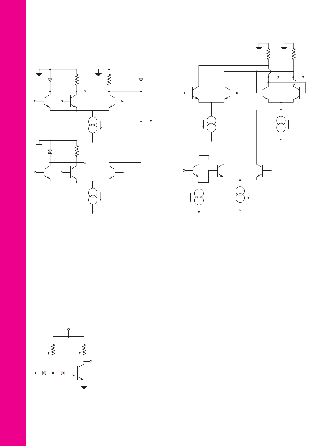
Figure P17.17
I
DC
–0.9 V
0.5 I
DC
–3 V
–3 V
–3 V–3 V
0.1 I
DC
0.1 I
DC
CLOCK
D
–0.2 V
–
Q
Q
RR
Figure P17.18
v
I
v
1
D
2
v
O
Q
O
i
1
i
3
i
2
R
1
=
12 kΩ
R
C
=
12 kΩ
D
1
V
CC
= 2.5 V
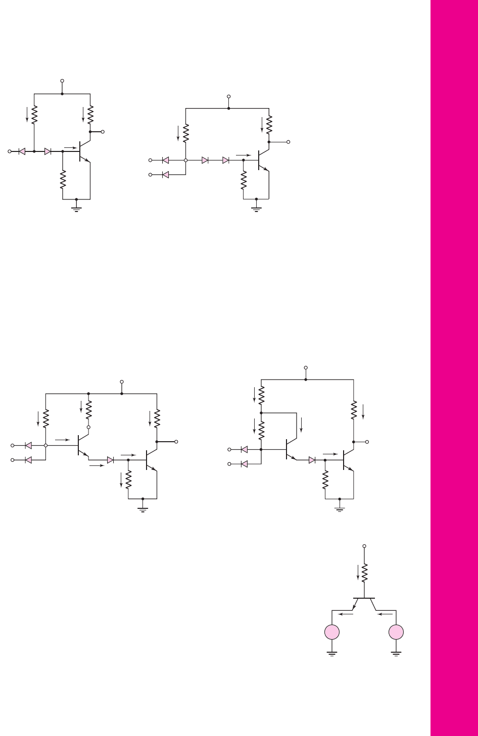
Figure P17.19
17.17 The input and output voltage levels for the circuit in Figure P17.17 are
compatible. (a) What are the logic 0 and logic 1 voltage levels? (b) What are
the logic functions implemented by this circuit at
v
O1
,
v
O2
, and
v
O3
?
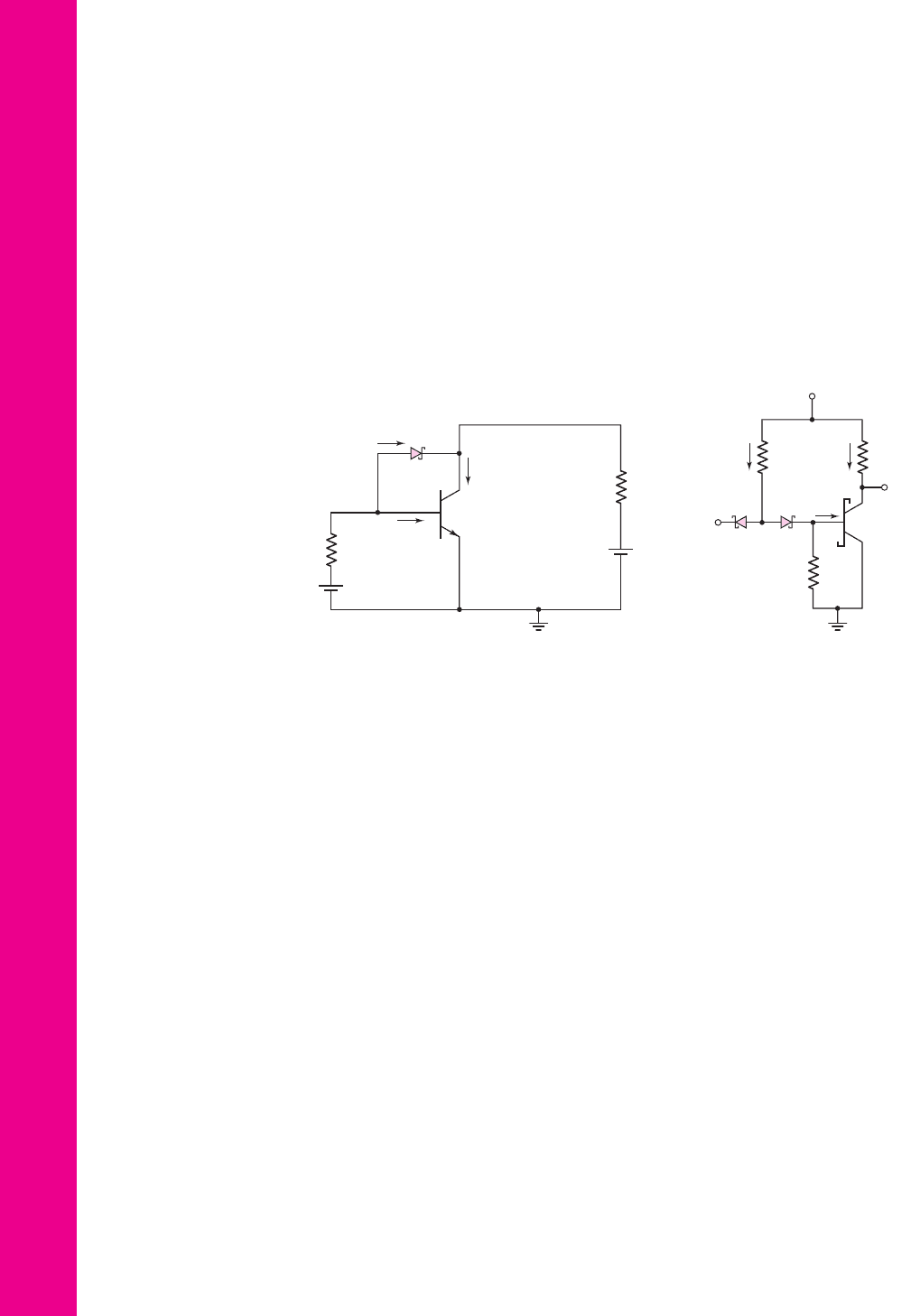
17.18 Consider the circuit in Figure P17.18. (a) Explain the operation of the
circuit. Demonstrate that the circuit functions as a clocked D flip-flop.
(b) Neglecting base currents, if
i
DC
= 50 μA
, calculate the maximum
power dissipated in the circuit.
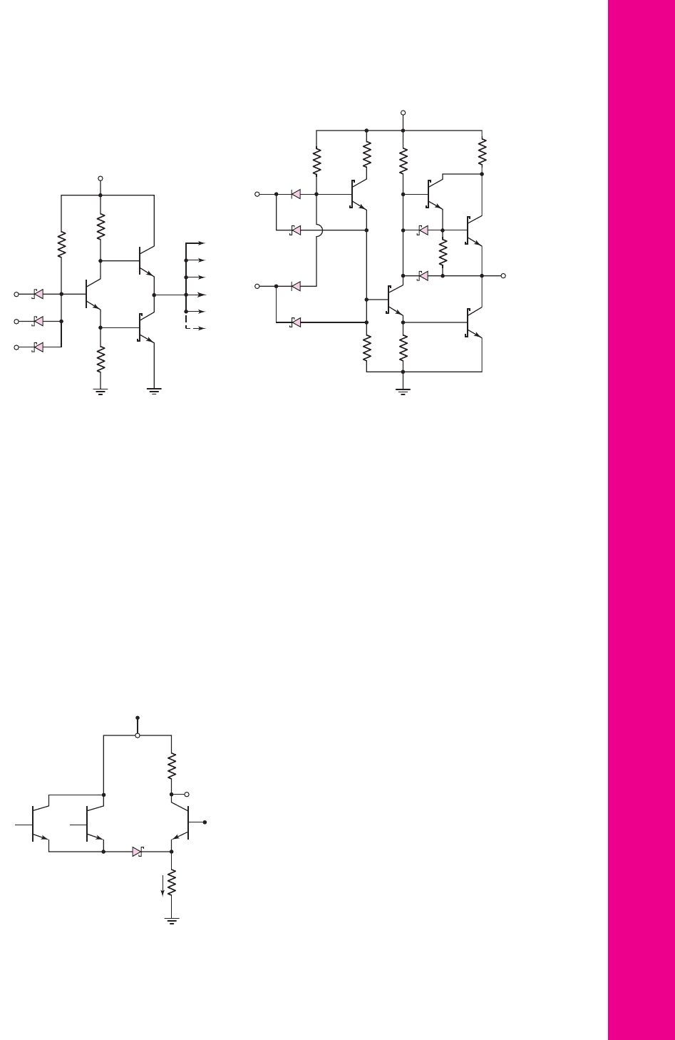
Section 17.3 Transistor–Transistor Logic
17.19 Consider the DTL circuit shown in Figure P17.19. Assume
β = 25
. (a) De-
termine the values of
i
1
,
i
2
,
i
3
,
v
1
, and
v
O
for (i)
v
I
= 0.1
V and
(ii)
v
I
= 2.5
V. (b) Determine the values of
v
I
and
v
1
at the point (i) where
Q
O
just begins to conduct and (ii) where
Q
O
just goes into saturation.
17.20 Consider the circuit in Figure P17.20. Assume transistor and diode parame-
ters:
β = 25
,
V
γ
= V
BE
(on) = 0.7
V,
V
BE
(sat) = 0.8V
, and
V
CE
(sat) =
0.1V
. Determine
v
1
,
i
1
,
i
B
,
i
C
, and
v
O
for (a)
v
I
= 0
and (b)
v
I
= 3.3V
.
17.21 In Figure P17.21, the transistor current gain is
β = 20
. Find the currents and
voltages
i
1
,
i
3
,
i
4
, and
v
for the input conditions: (i)
v
X
= v
Y
= 0.10 V
, and
(ii)
v
X
= v
Y
= 5V
.
17.22 Repeat Problem 17.21 for
V
CC
= 3.3
V. Assume input conditions of (i)
v
X
= v
Y
= 0.1
V and (ii)
v
X
= v
Y
= 3.3
V.
nea80644_ch17_1255-1314.qxd 8/6/09 11:12 AM Page 1308 pmath DATA-DISK:Desktop Folder:UDAYVEER/Neamen:
Chapter 17 Bipolar Digital Circuits 1309
i
B2
i
4
i
B1
i
3
i
5
i
1
i
2
V
CC
= 5 V
R
C
=
4.0 kΩ
R
2
= 2.0 kΩ
R
B
=
10 kΩ
R
1
=
4.0 kΩ
v
O
Q
o
Q
1
D
2
v
1
D
X
D
Y
v
X
v
Y
Figure P17.23
17.23 Figure P17.23 shows an improved version of the DTL circuit. One offset
diode is replaced by transistor
Q
1
, providing increased current drive to
Q
o
.
Assume
β = 20
for both transistors. (a) For
v
X
= v
Y
= 5V
, determine the
currents and voltages listed in the figure. (b) Calculate the maximum fanout
for the low output condition.
17.24 Repeat Problem 17.23 for
V
CC
= 3.3
V. Assume the input condition is
v
X
= v
Y
= 3.3
V.
17.25 For the modified DTL circuit in Figure P17.25, calculate the indicated
currents in the figure for
v
X
= v
Y
= 5V
.
17.26 The transistor
Q
1
in Figure P17.26 has parameters
β = 25
,
β
R
= 0.5
, and
V
BE
(on) = V
BC
(on) = 0.7V
. Find
i
B
,
i
C
, and
i
E
for (a)
v
I
= 0
, (b)
v
I
=
0.8V
, and (c)
v
I
= 3.6V
.
17.27 The parameters of the transistors in the circuit in Figure P17.27 are
β
F
≡ β = 25
and
β
R
= 0.1
. (a) Determine the values of
i
1
,
i
2
,
i
3
,
v
1
, and
v
O
for (i)
v
I
= 0.1
V and (ii)
v
I
= 2.5
V. (b) Determine the values of
v
I
and
v
1
at the point (i) where
Q
o
just begins to conduct and (ii) where
Q
o
just
goes into saturation.
20 kΩ
4 kΩ6 kΩ
V
+
= 3.3 V
v
I
v
O
i
C
i
B
i
1
v
1
Figure P17.20
i
4
i
3
i
1
V
CC
= 5 V
R
C
=
2.4 kΩ
R
B
= 15 kΩ
R
1
= 8 kΩ
v
O
Q
1
D
1
D
2
v
′
D
X
D
Y
v
X
v
Y
Figure P17.21
V
CC
= 5 V
R
C
= 6 kΩ
R
B
=
5 kΩ
R
2
=
2 kΩ
R
1
=
1.75 kΩ
v
O
Q
1
D
1
D
X
D
Y
v
X
v
Y
Q
o
i
1
i
3
i
2
i
Co
i
Bo
Figure P17.25
+5 V
R
B
= 6 kΩ
0.8 V
v
I
i
E
i
B
i
C
+
–
+
–
Q
1
Figure P17.26
nea80644_ch17_1255-1314.qxd 8/6/09 11:12 AM Page 1309 pmath DATA-DISK:Desktop Folder:UDAYVEER/Neamen:
1310 Part 3 Digital Electronics
17.28 For the transistors in the TTL circuit in Figure P17.28, the parameters
are
β
F
= 20
and
β
R
= 0
. (a) Determine the currents
i
1
,
i
2
,
i
3
,
i
4
,
i
B2
, and
i
B3
for the following input conditions: (i)
v
X
= v
Y
= 0.1V
, and (ii)
v
X
=
v
Y
= 5V
. (b) Show that for
v
X
= v
Y
= 5V
, transistors
Q
2
and
Q
3
are
biased in saturation.
17.29 The circuit configuration shown in Figure P17.21 is redesigned such that
V
CC
= 3.3
V,
R
1
= 16
k
,
R
C
= 6
k
, and
R
B
= 20
k
. Let
β = 50
.
(a) Determine
i
1
,
i
3
,
i
4
, and
v
for (i)
v
X
= 0.1
V,
v
Y
= 3.3
V and
(ii)
v
X
= v
Y
= 3.3
V. (b) Calculate the maximum fanout for the output low
condition such that
Q
1
remains biased in saturation. (c) Repeat part (b) if
the maximum collector current is limited to 5 mA.
17.30 In the TTLcircuit in Figure P17.30, the transistor parameters are
β
F
= 20
and
β
R
= 0.10
(for each input emitter). (a) Calculate the maximum fanout for
v
X
= v
Y
= 5V
. (b) Calculate the maximum fanout for
v
X
= v
Y
= 0.1V
.
(Assume
v
O
is allowed to decrease by 0.10 V from the no-load condition.)
17.31 For the TTL circuit in Figure P17.31, assume parameters of
β
F
= 50
,
β
R
= 0.1
,
V
BE
(on) = 0.7
V,
V
BE
(sat) = 0.8
V, and
V
CE
(sat) = 0.1
V.
(a) Determine
i
RB
,
i
RCP
,
i
Bo
, and
V
out
for (i)
V
in
= 0.1
V and (ii)
V
in
= 5
V.
v
I
v
O
Q
o
Q
1
i
1
i
3
i
2
R
1
=
12 kΩ
R
C
=
12 kΩ
V
CC
= 2.5 V
Figure P17.27
i
B2
i
B3
i
1
i
2
i
3
i
4
V
CC
= 5 V
R
3
=
2.2 kΩ
R
2
=
2.0 kΩ
R
B
= 1.5 kΩ
R
1
=
6.0 kΩ
Q
1
Q
2
Q
3
v
X
v
Y
v
O
Figure P17.28
V
CC
= 5 V
R
3
=
80 Ω
R
2
=
2.0 kΩ
R
B
=
1.5 kΩ
R
1
=
6.0 kΩ
Q
1
Q
2
Q
3
Q
4
D
1
v
X
v
Y
v
O
Figure P17.30
V
CC
= 5 V
R
B
Q
S
Q
I
Q
O
R
CP
4 kΩ
R
D
1 kΩ
1 kΩ
V
ou
t
V
in
Figure P17.31
nea80644_ch17_1255-1314.qxd 8/6/09 11:12 AM Page 1310 pmath DATA-DISK:Desktop Folder:UDAYVEER/Neamen:
Chapter 17 Bipolar Digital Circuits 1311
(b) For the case when five similar type load circuits are connected to the out-
put, calculate the power dissipated in the circuit shown for (i)
V
in
= 0.1
V
and (ii)
V
in
= 5
V.
17.32 Consider the basic TTL logic gate in Figure P17.32 with a fanout of 5.
Assume transistor parameters of
β
F
= 50
and
β
R
= 0.5
(for each input
emitter). Calculate the base and collector currents in each transistor for:
(a)
v
X
= v
Y
= v
Z
= 0.1V
, and (b)
v
X
= v
Y
= v
Z
= 5V
.
17.33 Consider the portion of the totem-pole output stage shown in Figure P17.33.
Let
β = 50
. (a) Determine
v
O
for (i)
I
L
= 5 μ
A, (ii)
I
L
= 5
mA, and
(iii)
I
L
= 25
mA. (b) Determine
I
L
if the output terminal is accidental
shorted to ground.
17.34 For the transistors in the TTL circuit in Figure P17.34, the parameters are
β
F
= 100
and
β
R
= 0.3
(for each input emitter). (a) For
v
X
= v
Y
= v
Z
=
2.8V
, determine
i
B1
,
i
B2
, and
i
B3
. (b) For
v
X
= v
Y
= v
Z
= 0.1V
, deter-
mine
i
B1
and
i
B4
for a fanout of 5.
17.35 A low-power TTL logic gate with an active pnp pull-up device is shown in
Figure P17.35. The transistor parameters are
β
F
= 100
and
β
R
= 0.2
(for
v
X
v
Y
v
Z
Q
1
Q
2
Q
3
3.9 kΩ
2.0 kΩ
0.8 kΩ
2.4 kΩ
v
O
+5 V
Figure P17.32
v
O
Q
4
R
3
=
2 kΩ
R
5
=
130 Ω
I
L
D
1
V
CC
= 5 V
Figure P17.33
v
X
v
Y
v
Z
0.9 kΩ
2 kΩ
0.5 kΩ
+2.8 V
Q
4
Q
3
Q
2
Q
1
v
O
1.0 kΩ
Figure P17.34
v
X
v
Y
v
Z
Q
1
Q
2
C
2
R
B1
=
1 kΩ
R
B2
=
1 kΩ
v
O
+2 V
Q
3
i
B1
i
B3
i
B2
Figure P17.35
nea80644_ch17_1255-1314.qxd 6/8/09 05:47 PM Page 1311 Aptara Inc.
1312 Part 3 Digital Electronics
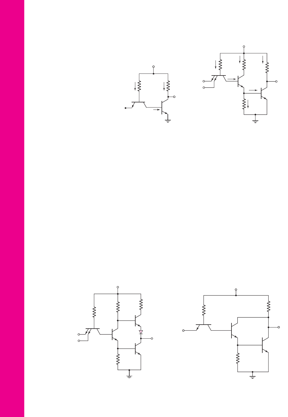
17.37 Let
β = 25
for the transistor in the circuit shown in Figure P17.37. (a) For
no load, determine the parameters
i
1
,
i
B
,
i
C
,
v
1
, and
v
O
when (i)
v
I
= 0
and
(ii)
v
I
= 1.5
V. (b) Determine
v
I
,
v
1
,
i
B
, and
i
C
for the case (i) where the
output transistor just begins to conduct and (ii) where the output transistor
just goes into saturation. (c) Assume that
N
similar type load circuits are
connected to the output. Determine the maximum number
N
such that the
output transistor remains in saturation.
17.38 Consider the Schottky TTL circuit in Figure 17.33. The transistor parame-
ters are
β
F
= 30
and
β
R
= 0.1
(for each emitter). (a) Determine all base
currents, collector currents, and node voltages for
v
X
= v
Y
= 0.4V
.
(b) Repeat part (a) for
v
X
= v
Y
= 3.6V
.
17.39 Consider the modified Schottky TTL NAND gate shown in Figure P17.39.
The current gain of all transistors is
β = 20
. (a) Assume
v
X
= v
Y
= v
Z
=
logic 1 and assume two similar type load circuits are connected to the out-
put. The transistor
Q
2
is biased in saturation with
i
B2
= 0.1
mA and
i
C2
= 0.2
mA. Determine the values of
R
B1
and
R
C1
. (b) Using the results
of part (a), and assuming
v
X
= 0.4
V and
v
Y
= v
Z
= 1.8
V, determine
v
B1
,
v
B2
,
v
O
, and all base and collector currents. Assume two similar type load
circuits are connected to the output. (c) Assume
v
X
= v
Y
= v
Z
=
logic 1
and assume four similar type load circuits are connected to the output.
Using the results of part (a), determine
v
B1
,
v
B2
,
v
O
, and all base and col-
lector currents. (d) Determine the maximum fanout for a low output state.
17.40 A low-power Schottky TTL logic circuit is shown in Figure P17.40. Assume
a transistor current gain of
β = 30
for all transistors. (a) Calculate the
each input emitter). Assume a fanout of 5. (a) For
v
X
= v
Y
= v
Z
= 0.1V
,
determine
i
B1
,
i
B2
,
i
B3
,
i
C2
, and
i
C3
. (b) Repeat part (a) for
v
X
= v
Y
=
v
Z
= 2V
.
Section 17.4 Schottky Transistor–Transistor Logic
17.36 Consider the Schottky transistor circuit in Figure P17.36. Assume parame-
ter values of
β = 50
,
V
BE
(on) = 0.7V
, and
V
γ
= 0.3
V for the Schottky
diode. (a) Determine
I
B
,
I
D
,
I
C
, and
V
CE
. (b) Remove the Schottky diode
and repeat part (a) assuming additional parameter values of
V
BE
(sat) =
0.8V
and
V
CE
(sat) = 0.1V
.
R
S
V
BB
I
B
I
D
I
C
10 kΩ
5.8 V
5 V
+
–
V
CC
+
–
R
C
1 kΩ
Figure P17.36
20 kΩ
1.2 kΩ1 kΩ
v
I
v
O
i
C
i
B
V
+
= 1.5 V
i
1
v
1
Figure P17.37
nea80644_ch17_1255-1314.qxd 8/6/09 11:12 AM Page 1312 pmath DATA-DISK:Desktop Folder:UDAYVEER/Neamen:
Chapter 17 Bipolar Digital Circuits 1313
maximum fanout for
v
X
= v
Y
= 3.6V
. (b) Using the results of part (a),
determine the power dissipated in the circuit for
v
X
= v
Y
= 3.6V
.
17.41 For all transistors in the circuit in Figure 17.35 in the text, the current gain
is
β = 50
. (a) Calculate the power dissipation in the circuit when the input
is at logic 0. (b) Repeat part (a) when the input is at logic 1. (c) Calculate the
output short-circuit current. (Assume the input is a logic 0 and the output is
inadvertently shorted to ground.)
17.42 Consider the circuit shown in Figure P17.42. Neglect base currents
and assume
V
BE
(on) = 0.7
V and
V
γ
= 0.3
V. (a) Determine
i
E
for
v
X
= v
Y
= 3
V. (b) Determine
i
E
and
R
C
for
v
X
= v
Y
= 2.4
V such that
v
O
= 2.4
V. (c) Using the results of parts (a) and (b), determine
the power dissipated in the circuit for (i)
v
X
= v
Y
= 3
V and
(ii)
v
X
= v
Y
= 2.4
V.
v
X
v
Y
10 kΩ
10 kΩ
4.1 kΩ
45 Ω
15 kΩ
10 kΩ
4.0 kΩ
Q
1
Q
2
Q
5
Q
3
Q
4
v
O
5 V
Figure P17.40
V
CC
= 2.5 V
R
B2
=
0.7 kΩ
R
C1
R
B1
Q
1
v
X
v
Y
v
Z
Q
3
v
O
Q
2
Figure P17.39
R
C
v
O
V
R
=
2.4 V
Q
R
v
Y
Q
B
v
X
Q
A
i
E
V
CC
= 3 V
R
E
=
2 kΩ
Figure P17.42
nea80644_ch17_1255-1314.qxd 6/8/09 06:49 PM Page 1313 Aptara Inc.

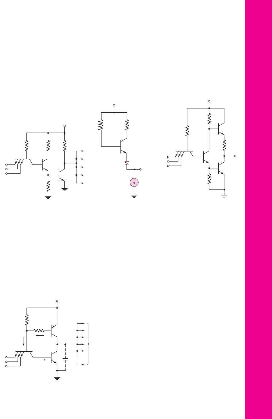
Section 17.5 BiCMOS Digital Circuits
17.43 Consider the basic BiCMOS inverter in Figure 17.36(a) in the text. As-
sume circuit and transistor parameters of
V
DD
= 5V
,
K
n
= K
p
= 0.1mA/V
2
,
V
TN
=+0.8V
,
V
TP
=−0.8
V, and
β = 50
. (a)
For
v
I
= 2.5V
, determine the current in each transistor. (b) If the current
calculated for
Q
1
were charging a 15 pF load capacitance, how long
would it take to charge the capacitance from 0 to 5 V? (c) Repeat part (b)
for the current in the transistor
M
P
.
17.44 Repeat Problem 17.43 for the BiCMOS inverter shown in Figure 17.36(b).
COMPUTER SIMULATION PROBLEMS
Using a computer simulation, generate the voltage transfer characteristics
of the modified ECL logic gate shown in Figure 17.10.
17.46 Using a computer simulation, generate the voltage transfer characteristics
of the basic DTL logic circuit shown in Figure 17.20.
17.47 Using a computer simulation, generate the voltage transfer characteristics
of the advanced low-power Schottky inverter gate shown in Figure 17.35.
17.48 Using a computer simulation, generate the voltage transfer characteristics
of the BiCMOS inverter shown in Figure 17.36(b).
DESIGN PROBLEMS
Design ECL series gating logic circuits, similar to the one shown in Figure
17.16, that will implement the logic functions (a)
Y =
[
A ·
(
B + C
)
+ D
]
and (b)
Y =
[
A · B + C · D
]
.
*D17.50 Design a clocked D flip-flop, using a modified ECL circuit design, such
that the output becomes valid on the negative-going edge of the clock
signal.
*D17.51 Design a low-power Schottky TTL exclusive-OR logic circuit.
*D17.52 Design a TTL R–S flip-flop.
1314 Part 3 Digital Electronics
nea80644_ch17_1255-1314.qxd 8/6/09 4:41 PM Page 1314 pmath DATA-DISK:Desktop Folder:untitled folder:
17.45
*D17.49

1315
APPENDIX
A
Physical Constants
and Conversion Factors
GENERAL CONSTANTS AND CONVERSION FACTORS
Angstrom Å 1 Å =
10
−4
μm = 10
−8
cm = 10
−10
m
Boltzmann’s constant k
k = 1.38 ×10
−23
J/K = 8.6 ×10
−5
eV/K
Electron–volt eV
1eV= 1.6 ×10
−19
J
Electronic charge e or q
q = 1.6 ×10
−19
C
Micron
μm1μm = 10
−4
cm = 10
−6
m
Mil
1 mil = 0.001 in. = 25.4 μm
Nanometer nm
1nm= 10
−9
m = 10
−3
μm = 10
Å
Permittivity of free space
ε
o
ε
o
= 8.85 ×10
−14
F/cm
Permeability of free
μ
o
μ
o
= 4π × 10
−9
H/cm
space
Planck’s constant h
h = 6.625 ×10
−34
J–s
Thermal voltage
V
T
V
T
= kT/q
∼
=
0.026 V at 300 K
Velocity of light in c
c = 2.998 ×10
10
cm/s
free space
SEMICONDUCTOR CONSTANTS
Si Ge GaAs SiO
2
Relative dielectric constant 11.7 16.0 13.1 3.9
Bandgap energy, E
g
(eV) 1.1 0.66 1.4
Intrinsic carrier concentration,
1.5 × 10
10
2.4 × 10
13
1.8 × 10
6
n
i
(cm
−3
at 300 K)
nea80644_appA_1315-1316.qxd 8/6/09 10:06 AM Page 1315 pmath DATA-DISK:Desktop Folder:UDAYVEER/Neamen:
nea80644_appA_1315-1316.qxd 8/6/09 10:06 AM Page 1316 pmath DATA-DISK:Desktop Folder:UDAYVEER/Neamen:

1317
APPENDIX
B
Selected Manufacturers’
Data Sheets
This appendix contains data sheets representative of transistors and op-amps. This
appendix is not meant as a substitute for the appropriate data books. In some cases,
therefore, only selected information is presented. These data sheets are provided
courtesy of National Semiconductor.
CONTENTS
1. 2N2222 npn Bipolar transistor
2. 2N2907 pnp Bipolar transistor
3. NDS9410 n-Channel enhancement-mode MOSFET
4. LM741 Operational amplifier
nea80644_appB_1317-1328.qxd 8/6/09 10:07 AM Page 1317 pmath DATA-DISK:Desktop Folder:UDAYVEER/Neamen: