Neamen D. Microelectronics: Circuit Analysis and Design
Подождите немного. Документ загружается.

118 Part 1 Semiconductor Devices and Basic Applications
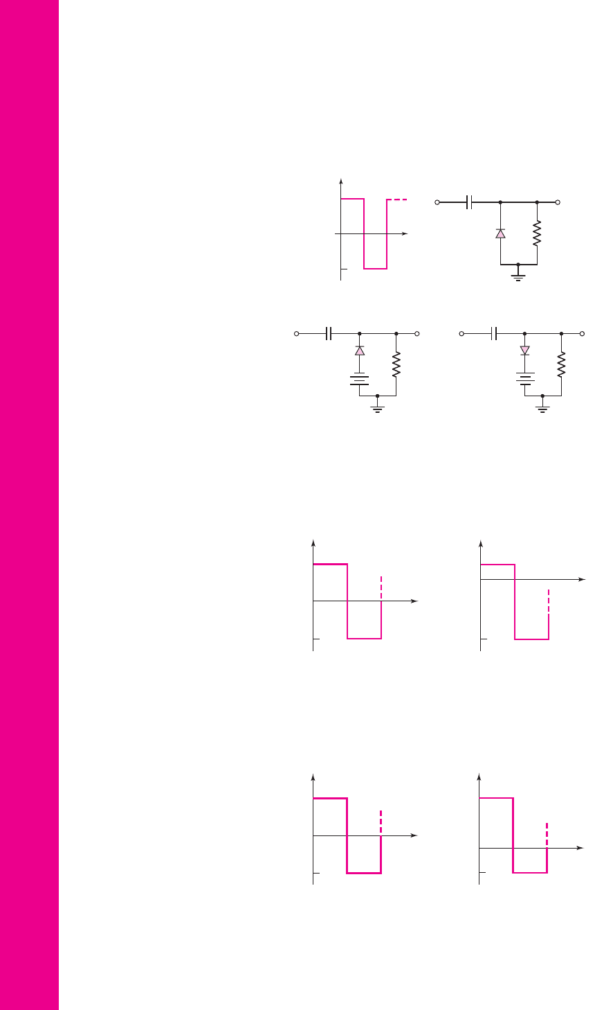
2.39 Sketch the steady-state output voltage
v
O
versus time for each circuit in
Figure P2.39 with the input voltage given in Figure P2.39(a). Assume
V
γ
= 0
and assume the
RC
time constant is large.
(b) (c)
v
O
+
–
R
C
V
B
= 5 V
v
I
v
O
+
–
R
C
V
B
= 5 V
v
I
R
v
O
20 V
–20 V
v
I
v
I
0
t
C
(a)
Figure P2.39
(a) (b)
v
I
t
–10 V
0
+10 V
v
O
t
–17.3 V
+2.7 V
0
Figure P2.40
–
(a) (b)
v
I
t
–20 V
0
+20 V
v
O
t
10 V
+30 V
0
Figure P2.41
D2.40 Design a diode clamper to generate a steady-state output voltage
v
O
from
the input voltage
v
I
shown in Figure P2.40 if (a)
V
γ
= 0
and (b)
V
γ
= 0.7
V.
D2.41 Design a diode clamper to generate a steady-state output voltage
v
O
from
the input voltage
v
I
in Figure P2.41 if
V
γ
= 0
.
nea80644_ch02_067-124.qxd 06/08/2009 08:42 PM Page 118 F506 Tempwork:Dont' Del Rakesh:June:Rakesh 06-08-09:MHDQ134-02 Folder:

Chapter 2 Diode Circuits 119
2.42 For the circuit in Figure P2.39(b), let
V
γ
= 0
and
v
I
= 10 sin ω t
(V). Plot
v
O
versus time over three cycles of input voltage. Assume the initial voltage
across the capacitor is zero and assume the
RC
time constant is very large.
2.43 Repeat Problem 2.42 for the circuit in Figure P2.39(c) for (i)
V
B
= 5
V and
(ii)
V
B
=−5
V.
Section 2.4 Multiple Diode Circuits
2.44 The diodes in the circuit in Figure P2.44 have piecewise linear parameters
of
V
γ
= 0.6
V and
r
f
= 0
. Determine the output voltage V
O
and the diode
currents
I
D1
and
I
D2
for the following input conditions: (a)
V
1
= 10
V,
V
2
= 0
; (b)
V
1
= 5
V,
V
2
= 0
; (c)
V
1
= 10
V,
V
2
= 5
V; and (d)
V
1
=
V
2
= 10
V. (e) Compare the results of parts (a) through (d) with a computer
simulation analysis.
2.45 In the circuit in Figure P2.45 the diodes have the same piecewise linear pa-
rameters as described in Problem 2.44. Calculate the output voltage V
O
and
the currents
I
D1
,
I
D2
, and I for the following input conditions: (a)
V
1
=
V
2
= 10
V; (b)
V
1
= 10
V,
V
2
= 0
; (c)
V
1
= 10
V,
V
2
= 5
V; and (d)
V
1
= V
2
= 0
.
V
1
V
2
V
O
D
1
D
2
I
D1
I
D2
0.5 k Ω
0.5 kΩ
9.5 kΩ
Figure P2.44
V
1
V
2
V
O
D
1
D
2
I
D1
I
I
D2
0.5 kΩ
0.5 k Ω
9.5 kΩ
+10 V
Figure P2.45
V
1
V
2
V
O
D
1
D
2
D
3
I
D1
I
I
D2
I
D3
0.5 kΩ
0.5 kΩ
9.5 kΩ
+10 V
+5 V
Figure P2.46
2.46 The diodes in the circuit in Figure P2.46 have the same piecewise linear
parameters as described in Problem 2.44. Determine the output voltage V
O
and the currents
I
D1
,
I
D2
,
I
D3
, and I for the following input conditions: (a)
V
1
= V
2
= 0
; (b)
V
1
= V
2
= 5
V; (c)
V
1
= 5
V,
V
2
= 0
; and (d)
V
1
= 5
V,
V
2
= 2
V.
nea80644_ch02_067-124.qxd 06/08/2009 07:29 PM Page 119 F506 Tempwork:Dont' Del Rakesh:June:Rakesh 06-08-09:MHDQ134-02 Folder:
120 Part 1 Semiconductor Devices and Basic Applications
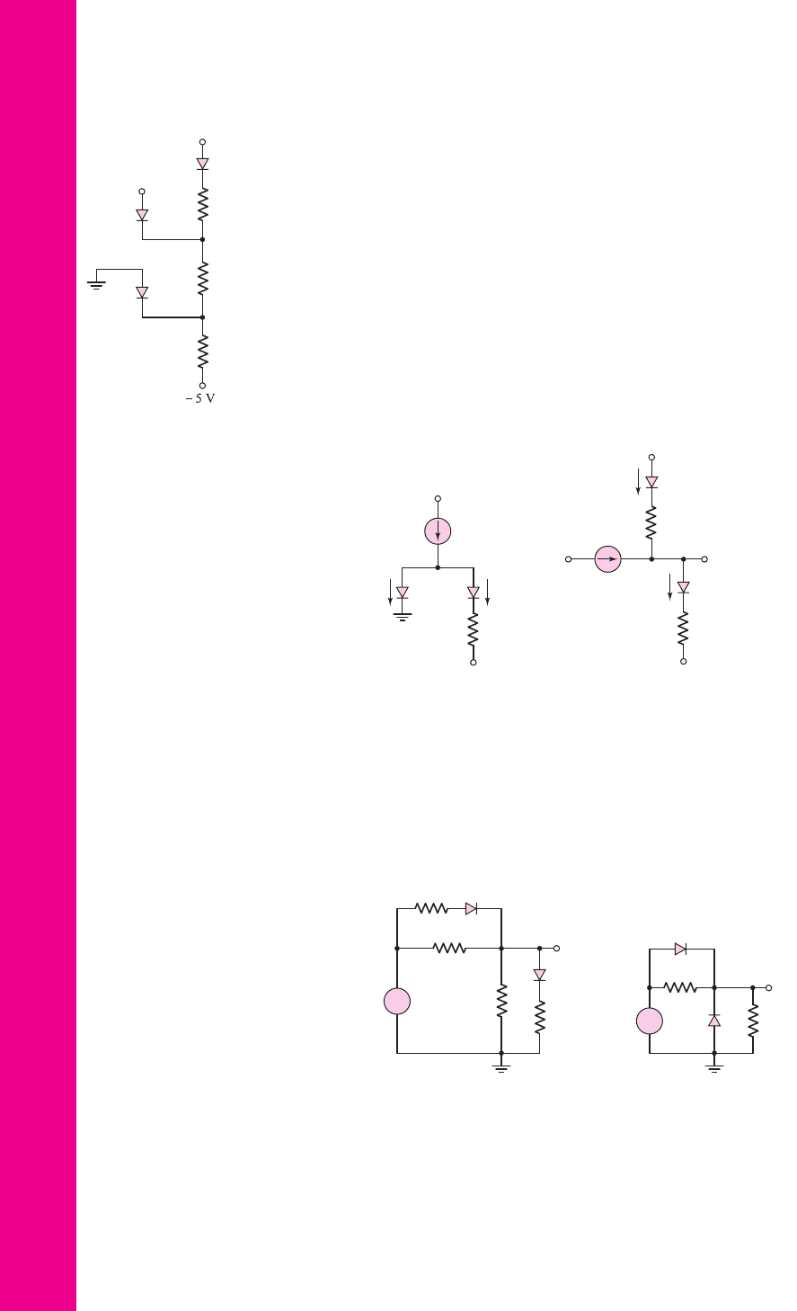
2.47 Consider the circuit shown in Figure P2.47. Assume each diode cut-in volt-
age is
V
γ
= 0.6
V. (a) Determine
R
1
,
R
2
, and
R
3
such that
I
D1
= 0.2
mA,
I
D2
= 0.3
mA, and
I
D3
= 0.5
mA. (b) Find
V
1
,
V
2
, and each diode current
for
R
1
= 10
k
,
R
2
= 4
k
, and
R
3
= 2.2
k
. (c) Repeat part (b) for
R
1
= 3
k
,
R
2
= 6
k
, and
R
3
= 2.5
k
. (d) Repeat part (b) for
R
1
= 6
k
,
R
2
= 3
k
, and
R
3
= 6
k
.
2.48 The diode cut-in voltage for each diode in the circuit shown in Figure P2.48
is 0.7 V. Determine the value of
R
such that (a)
I
D1
= I
D2
, (b)
I
D1
= 0.2I
D2
,
and (c)
I
D1
= 5I
D2
.
2.49 Consider the circuit in Figure P2.49. Each diode cut-in voltage is
V
γ
= 0.7
V. (a) For
R
2
= 1.1
k
, determine
I
D1
,
I
D2
, and
V
A
. (b) Repeat
part (a) for
R
2
= 2.5
k
. (c) Find
R
2
such that
V
A
= 0
. What are the values
of
I
D1
and
I
D2
?
2.50 In each circuit shown in Figure P2.50, the diode cut-in voltage is
V
γ
= 0.6
V. (a) For the circuit in Figure P2.50(a), determine
v
O
for (i)
v
I
=+5
V and (ii)
v
I
=−5
V. (b) Repeat part (a) for the circuit in Figure
P2.50(b). (c) Plot the voltage transfer characteristics,
v
O
versus
v
I
, of each
circuit over the range
−5 ≤ v
I
≤+5
V.
I =
5 mA
D
1
D
2
R
I
D1
I
D2
+5 V
–2 V
Figure P2.48
I = 5 mA
R
1
=
2 kΩ
D
2
R
2
V
A
I
D2
D
1
I
D1
+5 V
10 V
–5 V
Figure P2.49
D
1
D
2
D
3
V
1
V
2
R
1
R
2
R
3
+10 V
+5 V
Figure P2.47
5 kΩ
5 kΩ
500 Ω
500 Ω
D
2
D
1
v
I
v
O
+
–
2 kΩ
2 kΩ
D
1
D
2
v
I
v
O
+
–
(a) (b)
Figure P2.50
*2.51 Assume
V
γ
= 0.7
V for each diode in the circuit in Figure P2.51. Plot
v
O
versus
v
I
for
−10 ≤ v
I
≤+10
V.
nea80644_ch02_067-124.qxd 06/08/2009 07:29 PM Page 120 F506 Tempwork:Dont' Del Rakesh:June:Rakesh 06-08-09:MHDQ134-02 Folder:
Chapter 2 Diode Circuits 121
10 kΩ
10 kΩ
10 kΩ
+10 V
–10 V
v
I
v
O
Figure P2.51
V
A
V
O
R
2
=
2 kΩ
R
1
=
6.15 kΩ
D
3
R
4
I
D3
–10 V
D
2
D
1
R
3
I
D2
I
D1
–5 V
+15 V
Figure P2.52
V
O
+10 V
–10 V
R
1
R
2
D
2
D
1
I
D1
Figure P2.53
2.52 The cut-in voltage of each diode in the circuit shown in Figure P2.52 is
V
γ
= 0.7
V. Determine
I
D1
,
I
D2
,
I
D3
, and
V
A
for (a)
R
3
= 14
k
,
R
4
= 24
k
; (b)
R
3
= 3.3
k
,
R
4
= 5.2
k
; and (c)
R
3
= 3.3
k
,
R
4
= 1.32
k
.
2.53 Let
V
γ
= 0.7
V for each diode in the circuit in Figure P2.53. (a) Find
I
D1
and V
O
for
R
1
= 5k
and
R
2
= 10 k
. (b) Repeat part (a) for
R
1
= 10 k
and
R
2
= 5k
.
2.54 For the circuit shown in Figure P2.54, let
V
γ
= 0.7
V for each diode. Calculate
I
D1
and V
O
for (a)
R
1
= 10 k
,
R
2
= 5k
and for (b)
R
1
= 5k
,
R
2
= 10 k
.
2.55 Assume each diode cut-in voltage is
V
γ
= 0.7
V for the circuit in Figure
P2.55. Determine
I
D1
and V
O
for (a)
R
1
= 10 k
,
R
2
= 5k
and (b)
R
1
= 5k
,
R
2
= 10 k
.
V
O
+10 V
–15 V
R
1
R
2
D
2
D
1
I
D1
Figure P2.54
V
O
+10 V
–15 V
R
1
R
2
D
2
D
1
I
D1
Figure P2.55
V
O
+15
10 kΩ
20 kΩ
20 kΩ
I
D
Figure P2.56
2.56 If
V
γ
= 0.7
V for the diode in the circuit in Figure P2.56 determine I
D
and V
O
.
nea80644_ch02_067-124.qxd 06/08/2009 07:29 PM Page 121 F506 Tempwork:Dont' Del Rakesh:June:Rakesh 06-08-09:MHDQ134-02 Folder:
122 Part 1 Semiconductor Devices and Basic Applications
2.57 Let
V
γ
= 0.7
V for the diode in the circuit in Figure P2.57. Determine
I
D
,
V
D
,
V
A
, and
V
B
for (a)
V
1
= V
2
= 6
V; (b)
V
1
= 2
V,
V
2
= 5
V; (c)
V
1
= 5
V,
V
2
= 4
V; and (d)
V
1
= 2
V,
V
2
= 8
V.
V
D
10 kΩ
V
2
V
1
10 kΩ
10 kΩ 10 kΩ
– +
I
D
Figure P2.57
2.58 (a) Each diode in the circuit in Figure P2.58 has piecewise linear parameters
of
V
γ
= 0
and
r
f
= 0
. Plot
v
O
versus
v
I
for
0 ≤ v
I
≤ 30
V. Indicate the
breakpoints and give the state of each diode in the various regions of the plot.
(b) Compare the results of part (a) with a computer simulation analysis.
2.59 Each diode cut-in voltage in the circuit in Figure P2.59 is 0.7 V. Determine
I
D1
,
I
D2
,
I
D3
, and
v
O
for (a)
v
I
= 0.5
V, (b)
v
I
= 1.5
V, (c)
v
I
= 3.0
V, and
(d)
v
I
= 5.0
V.
R
2
=
8 kΩ
R
1
= 4 kΩ
I
D1
I
D2
R
3
=
6 kΩ
v
I
+
–
D
1
D
2
1.0 V
+
–
I
D3
R
4
=
4 kΩ
D
3
2.0 V
+
–
v
O
Figure P2.59
I =
100 mA
I
D2
v
I
D
1
+12 V
V
B
+
–
D
2
Figure P2.60
D
2
V
2
V
1
V
O1
V
O2
D
1
D
4
D
3
0 V
10 kΩ 10 kΩ
Figure P2.61
+
–
v
I
+
5 kΩ
10 V
+
––
–
v
O
D
1
D
2
10 kΩ
15 kΩ
2.5 V
+
–
Figure P2.58
2.60 Let
V
γ
= 0.7
V for each diode in the circuit shown in Figure P2.60. Plot
I
D2
versus
v
I
over the range
0 ≤ v
I
≤ 12
V for (a)
V
B
= 4.5
V and (b)
V
B
= 9
V.
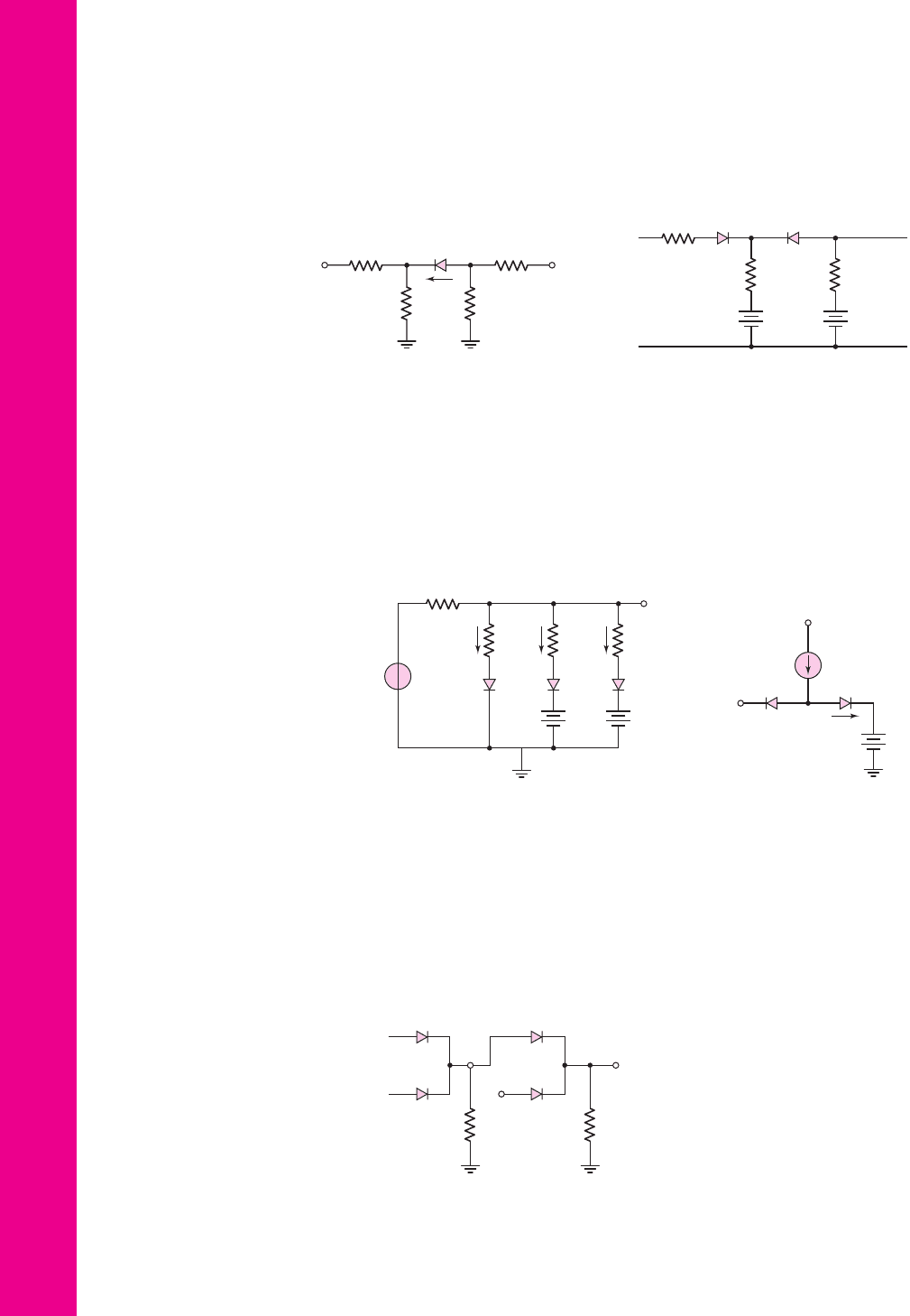
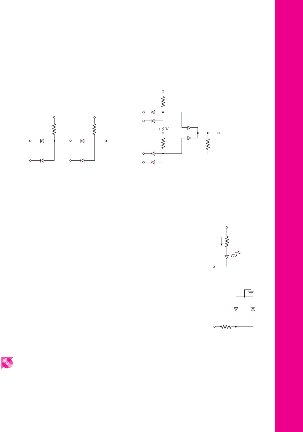
2.61 Consider the circuit in Figure P2.61. The output of a diode OR logic gate is
connected to the input of a second diode OR logic gate. Assume
V
γ
= 0.6
V
for each diode. Determine the outputs
V
O1
and
V
O2
for: (a)
V
1
= V
2
= 0
;
(b)
V
1
= 5V
,
V
2
= 0
; and (c)
V
1
= V
2
= 5
V. What can be said about the
relative values of
V
O1
and
V
O2
in their “high” state?
nea80644_ch02_067-124.qxd 06/08/2009 07:29 PM Page 122 F506 Tempwork:Dont' Del Rakesh:June:Rakesh 06-08-09:MHDQ134-02 Folder:
Chapter 2 Diode Circuits 123
2.62 Consider the circuit in Figure P2.62. The output of a diode AND logic gate
is connected to the input of a second diode AND logic gate. Assume
V
γ
=
0.6 V for each diode. Determine the outputs
V
O1
and
V
O2
for: (a)
V
1
=
V
2
= 5
V; (b)
V
1
= 0
,
V
2
= 5
V; and (c)
V
1
= V
2
= 0
. What can be said
about the relative values of
V
O1
and
V
O2
in their “low” state?
V
1
V
O1
V
O2
D
1
D
3
D
2
10 kΩ
+5 V
5 V
V
2
D
4
10 kΩ
+5 V
Figure P2.62
V
O
V
1
V
2
V
3
V
4
+ 5 V
10 kΩ
10 kΩ
10 kΩ
Figure P2.63
2.63 Determine the Boolean expression for V
O
in terms of the four input voltages
for the circuit in Figure P2.63 (Hint: A truth table might be helpful.)
Section 2.5 LED and Photodiode Circuits
2.64 Consider the circuit shown in Figure P2.64. The forward-bias cut-in voltage
of the diode is 1.5 V and the forward-bias resistance is
r
f
= 10
. Deter-
mine the value of R required to limit the current to
I = 12
mA when
V
I
= 0.2
V.
2.65 The light-emitting diode in the circuit shown in Figure P2.64 has parame-
ters
V
γ
= 1.7
V and
r
f
= 0
. Light will first be detected when the current is
I = 8
mA. If
R = 750
, determine the value of V
I
at which light will first
be detected.
2.66 The parameters of
D
1
and
D
2
in the circuit shown in Figure P2.66 are
V
γ
= 1.7
V and
r
f
= 20
. The current in each diode is to be limited to
I
D
= 15
mA for
V
I
=±5
V. Determine the required value of
R
.
2.67 If the resistor in Example 2.12 is
R = 2k
and the diode is to be reverse
biased by at least 1 V, determine the minimum power supply voltage
required.
2.68 Consider the photodiode circuit shown in Figure 2.44. Assume the quantum
efficiency is 1. A photocurrent of 0.6 mA is required for an incident photon
flux of
= 10
17
cm
−2
–s
−1
. Determine the required cross-sectional area of
the diode.
COMPUTER SIMULATION PROBLEMS
2.69 Consider the voltage doubler circuit in Figure 2.14. Assume a 60 Hz,
120 V (rms) signal is applied at the input of the transformer with a 20:1
turns ratio. Let
R = 10
k
and
C
1
= C
2
= 200 μ
F. Using a computer
simulation, plot the output voltage over four cycles of input voltage.
V
I
V
CC
= 10 V
R
I
Figure P2.64
V
I
D
1
D
2
R
Figure P2.66
nea80644_ch02_067-124.qxd 06/08/2009 07:29 PM Page 123 F506 Tempwork:Dont' Del Rakesh:June:Rakesh 06-08-09:MHDQ134-02 Folder:

1.7 5
v
I
(V)
v
O
(V)
2.5
1.7
–4.2
–3.2
–5
–3.2
Figure P2.76
124 Part 1 Semiconductor Devices and Basic Applications
2.70 Consider the parameters and results of Example 2.2. Use a computer simu-
lation to plot the output voltage of each rectifier over four cycles of input
voltage. Also determine the PIV of each diode. How do the computer results
compare with the results of the example?
2.71 (a) Using a computer simulation, verify the results of Exercise TYU2.3.
(b) Determine the ripple voltage if a filter capacitance of
C = 50 μ
F is con-
nected in parallel with the load resistance.
2.72 (a) Using a computer simulation, determine each diode current and voltage
in the circuit shown in Figure 2.40. (b) Repeat part (a) using the circuit
parameters given in Exercise 2.11.
DESIGN PROBLEMS
*D2.73 Consider the full-wave bridge rectifier circuit. The input signal is 120 V
(rms) at 60 Hz. The load resistance is
R
L
= 250
. The peak output voltage
is to be 9 V and the ripple voltage is to be no more than 5 percent. Determine
the required turns ratio and the required value of filter capacitance.
*D2.74 Design a simple dc voltage source using a 120 V (rms), 60 Hz input signal
to a nominal 10 V output signal. A Zener diode with parameters
V
ZO
= 10
V and
r
z
= 3
is available. The rated power of the Zener diode
is 5 W. The source regulation is to be limited to 2 percent.
*D2.75 A clipper is to be designed such that
v
O
= 2.5
V for
v
I
≥ 2.5
V and
v
O
=−1.25
V for
v
I
≤−1.25
V.
*D2.76 Design a circuit to provide the voltage transfer characteristics shown in
Figure P2.76. Use diodes and Zener diodes with appropriate breakdown
voltages in the design. The maximum current in the circuit is to be limited
to 1mA.
nea80644_ch02_067-124.qxd 06/10/2009 07:47 PM Page 124 F506 Tempwork:Dont' Del Rakesh:June:Rakesh 06-10-09:MHDQ134-02:

Chapter
The Field-Effect
Transistor
3
3
In this chapter, we introduce a major type of transistor, the metal-oxide-semiconductor
field-effect transistor (MOSFET). The MOSFET led to the electronics revolution of
the 1970s and 1980s, in which the microprocessor made possible powerful desktop
computers, laptop computers, sophisticated handheld calculators, iPods, and a
plethora of other electronic systems. The MOSFET can be made very small, so high-
density very large scale integration (VLSI) circuits and high-density memories are
possible.
Two complementary devices, the n-channel MOSFET (NMOS) and the p-channel
MOSFET (PMOS), exist. Each device is equally important and allows a high degree
of flexibility in electronic circuit design. The
i–v
characteristics of these devices
are introduced, and the dc analysis and design techniques of MOSFET circuits are
developed.
Another type of field-effect transistor is the junction FET. There are two general
categories of junction field-effect transistors (JFETs)—the pn junction FET (pn
JFET) and the metal-semiconductor field-effect transistor (MESFET), which is fab-
ricated with a Schottky barrier junction. JFETs were developed before MOSFETs,
but the applications and uses of MOSFETs have far surpassed those of the JFET.
However, we will consider a few JFET circuits in this chapter.
PREVIEW
In this chapter, we will:
• Study and understand the structure, operation, and characteristics of the vari-
ous types of MOSFETs.
• Understand and become familiar with the dc analysis and design techniques
of MOSFET circuits.
• Examine three applications of MOSFET circuits.
• Investigate current source biasing of MOSFET circuits, such as those used in
integrated circuits.
• Analyze the dc biasing of multistage or multitransistor circuits.
• Understand the operation and characteristics of the junction field-effect tran-
sistor, and analyze the dc response of JFET circuits.
• As an application, incorporate a MOS transistor in a circuit design that en-
hances the simple diode electronic thermometer discussed in Chapter 1.
125
nea80644_ch03_125-204.qxd 06/08/2009 08:36 PM Page 125 F506 Hard disk:Desktop Folder:MHDQ134-03:

126 Part 1 Semiconductor Devices and Basic Applications
1
The capacitance of a parallel plate capacitor, neglecting fringing fields, is
C = A/d
, where A is the area
of one plate, d is the distance between plates, and
is the permittivity of the medium between the plates.
3.1 MOS FIELD-EFFECT TRANSISTOR
Objective: • Understand the operation and characteristics of the
various types of metal-oxide semiconductor field-effect transistors
(MOSFETs).
The metal-oxide-semiconductor field-effect transistor (MOSFET) became a
practical reality in the 1970s. The MOSFET, compared to BJTs, can be made very
small (that is, it occupies a very small area on an IC chip). Since digital circuits can
be designed using only MOSFETs, with essentially no resistors or diodes required,
high-density VLSI circuits, including microprocessors and memories, can be fabri-
cated. The MOSFET has made possible the handheld calculator, the powerful
personal computer, and the laptop computer. MOSFETs can also be used in analog
circuits, as we will see in the next chapter.
In the MOSFET, the current is controlled by an electric field applied perpendic-
ular to both the semiconductor surface and to the direction of current. The phenome-
non used to modulate the conductance of a semiconductor, or control the current in a
semiconductor, by applying an electric field perpendicular to the surface is called the
field effect. The basic transistor principle is that the voltage between two terminals
controls the current through the third terminal.
In the following two sections, we will discuss the various types of MOSFETs,
develop the i–
v
characteristics, and then consider the dc biasing of various MOSFET
circuit configurations. After studying these sections, you should be familiar and com-
fortable with the MOSFET and MOSFET circuits.
Two-Terminal MOS Structure
The heart of the MOSFET is the metal-oxide-semiconductor capacitor shown in
Figure 3.l. The metal may be aluminum or some other type of metal. In most cases,
the metal is replaced by a high-conductivity polycrystalline silicon layer deposited
on the oxide. However, the term metal is usually still used in referring to MOSFETs.
In the figure, the parameter
t
ox
is the thickness of the oxide and
ox
is the oxide
permittivity.
The physics of the MOS structure can be explained with the aid of a simple
parallel-plate capacitor.
1
Figure 3.2(a) shows a parallel-plate capacitor with the top
plate at a negative voltage with respect to the bottom plate. An insulator material
separates the two plates. With this bias, a negative charge exists on the top plate, a
positive charge exists on the bottom plate, and an electric field is induced between the
two plates, as shown.
A MOS capacitor with a p-type semiconductor substrate is shown in Figure 3.2(b).
The top metal terminal, also called the gate, is at a negative voltage with respect to the
semiconductor substrate. From the example of the parallel-plate capacitor, we can
see that a negative charge will exist on the top metal plate and an electric field will
be induced in the direction shown in the figure. If the electric field penetrates the
3.1.1
nea80644_ch03_125-204.qxd 06/08/2009 08:36 PM Page 126 F506 Hard disk:Desktop Folder:MHDQ134-03:
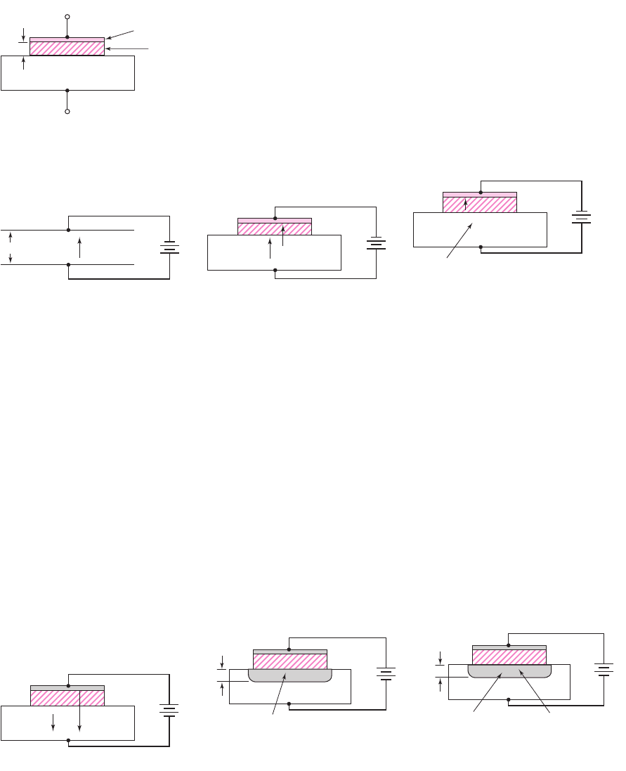
Chapter 3 The Field-Effect Transistor 127
p-type h
+
E-field
–
+
––––––
V
p-type
–
+
––––––
++++++
V
Accumulation
layer of holes
(a) (b) (c)
–
+
––––––
++++++
VE-field
d
e
E-field
Figure 3.2 (a) A parallel-plate capacitor, showing the electric field and conductor charges,
(b) a corresponding MOS capacitor with a negative gate bias, showing the electric field and
charge flow, and (c) the MOS capacitor with an accumulation layer of holes
semiconductor, the holes in the p-type semiconductor will experience a force toward
the oxide-semiconductor interface. The equilibrium distribution of charge in the
MOS capacitor with this particular applied voltage is shown in Figure 3.2(c).An accu-
mulation layer of positively charged holes at the oxide-semiconductor interface
corresponds to the positive charge on the bottom “plate” of the MOS capacitor.
Figure 3.3(a) shows the same MOS capacitor, but with the polarity of the applied
voltage reversed. A positive charge now exists on the top metal plate and the in-
duced electric field is in the opposite direction, as shown. In this case, if the electric
field penetrates the semiconductor, holes in the p-type material will experience a force
away from the oxide-semiconductor interface. As the holes are pushed away from the
interface, a negative space-charge region is created, because of the fixed acceptor
impurity atoms. The negative charge in the induced depletion region corresponds to
the negative charge on the bottom “plate” of the MOS capacitor. Figure 3.3(b) shows
the equilibrium distribution of charge in the MOS capacitor with this applied voltage.
(a) (b) (c)
p-type
+
–
+ + + +
V
E-field
h
+
+
–
V
p-type
++++
Induced negative
space-charge
region
x
d
layer
p-type
+
–
++++++
V
Induced negative
space-charge
region
Electron
inversion
x
dT
––––––
Figure 3.3 The MOS capacitor with p-type substrate: (a) effect of positive gate bias,
showing the electric field and charge flow, (b) the MOS capacitor with an induced space-
charge region due to a moderate positive gate bias, and (c) the MOS capacitor with an
induced space-charge region and electron inversion layer due to a larger positive gate bias
Semiconductor
substrate
t
ox
Metal
Insulator
(oxide)
Substrate or
bod
y
terminal
Gate terminal
e
ox
Figure 3.1 The basic MOS capacitor structure
nea80644_ch03_125-204.qxd 06/08/2009 08:36 PM Page 127 F506 Hard disk:Desktop Folder:MHDQ134-03: