Neamen D. Microelectronics: Circuit Analysis and Design
Подождите немного. Документ загружается.

138 Part 1 Semiconductor Devices and Basic Applications
G
+
–
+
v
SD
i
D
v
SG
G
S
D
(b)
+
–
+
v
SD
i
D
v
SG
G
S
D
(c)
+
–
+
–
––
v
DS
i
D
v
SG
B
S
D
(a)
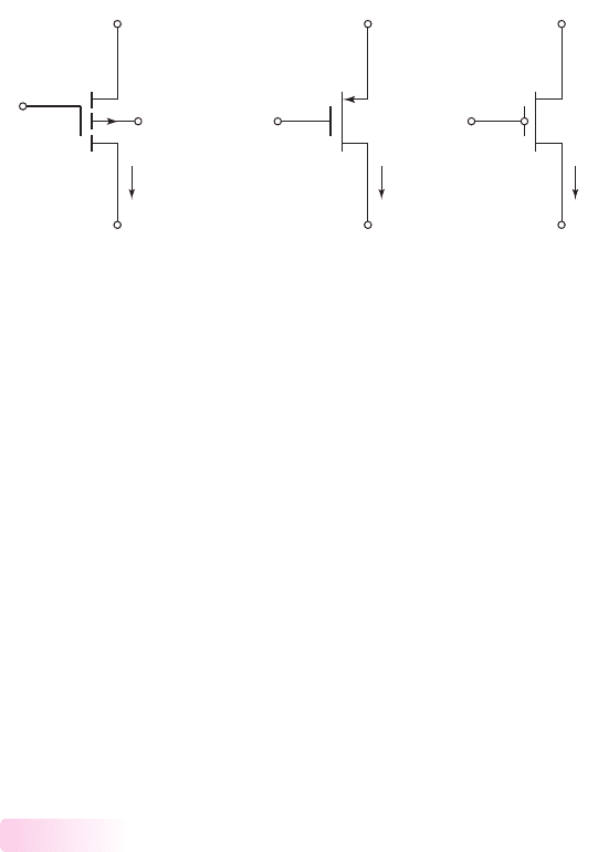
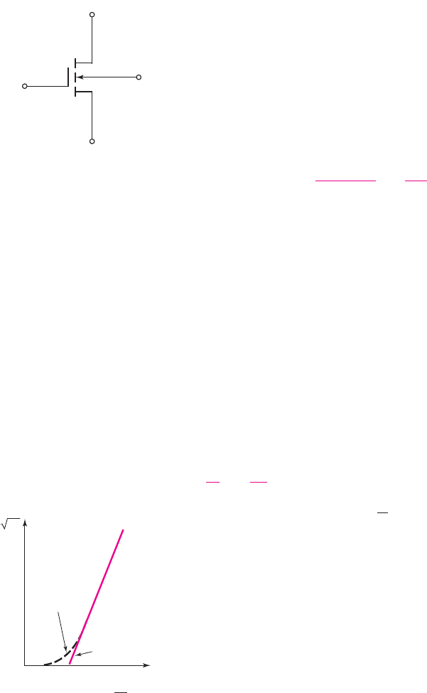
Figure 3.13 The p-channel enhancement-mode MOSFET: (a) conventional circuit symbol,
(b) circuit symbol that will be used in this text, and (c) a simplified circuit symbol used in
more advanced texts
The conventional circuit symbol for the p-channel enhancement-mode
MOSFET appears in Figure 3.13(a). Note that the arrowhead direction on the sub-
strate terminal is reversed from that in the n-channel enhancement-mode device.
This circuit symbol again shows the four terminal structure of the MOSFET device.
The circuit symbol for the p-channel enhancement-mode device shown in Fig-
ure 3.13(b) will be used in this text. The arrowhead is on the source terminal indicating
the direction of the current, which for the p-channel device is into the source terminal.
In more advanced texts and journal articles, the circuit symbol of the p-channel
MOSFET shown in Figure 3.13(c) is generally used. Again, the gate terminal is
obvious but includes the O symbol to indicate that this is a PMOS device. It is
implicitly understood that the “top” terminal is the source and the “bottom” terminal
is the drain. The top terminal, in this case the source, is normally at a higher poten-
tial than the bottom terminal. Again, in this text, we will use the symbol shown in
Figure 3.13(b) for clarity.
Additional MOSFET Structures and Circuit Symbols
Before we start analyzing MOSFET circuits, there are two other MOSFET struc-
tures in addition to the n-channel enhancement-mode device and the p-channel
enhancement-mode device that need to be considered.
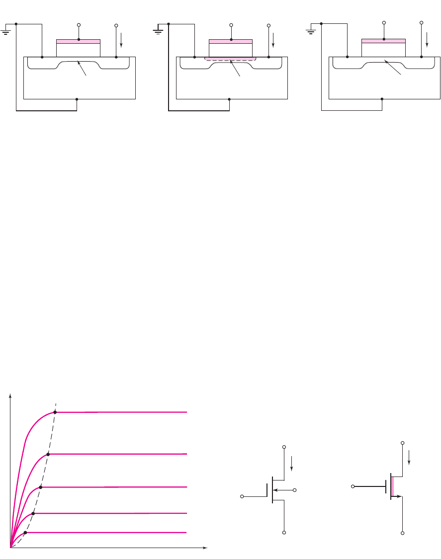
n-Channel Depletion-Mode MOSFET
Figure 3.14(a) shows the cross section of an n-channel depletion-mode MOSFET.
When zero volts are applied to the gate, an n-channel region or inversion layer exists
under the oxide as a result, for example, of impurities introduced during device
fabrication. Since an n-region connects the n-source and n-drain, a drain-to-source cur-
rent may be generated in the channel even with zero gate voltage. The term depletion
mode means that a channel exists even at zero gate voltage. A negative gate voltage
must be applied to the n-channel depletion-mode MOSFET to turn the device off.
Figure 3.14(b) shows the n-channel depletion mode MOSFET with a negative
applied gate-to-source voltage. A negative gate voltage induces a space-charge
region under the oxide, thereby reducing the thickness of the n-channel region.
The reduced thickness decreases the channel conductance, which in turn reduces
the drain current. When the gate voltage is equal to the threshold voltage, which is
3.1.7
nea80644_ch03_125-204.qxd 06/08/2009 08:37 PM Page 138 F506 Hard disk:Desktop Folder:MHDQ134-03:
Chapter 3 The Field-Effect Transistor 139
(a) (b) (c)
p-type
n-channel
G
S
D
v
GS
= 0 +v
DS
i
D
n
+
n
+
p-type
Depletion
region
G
S
D
V
TN
< v
GS
< 0 +v
DS
i
D
n
+
n
+
p-type
Electron
accumulation
layer
G
S
D
v
GS
> 0
+v
DS
i
D
–––––
n
+
n
+
Figure 3.14 Cross section of an n-channel depletion mode MOSFET for: (a)
v
GS
= 0
,
(b)
v
GS
< 0
, and (c)
v
GS
> 0
negative for this device, the induced space-charge region extends completely through
the n-channel region, and the current goes to zero. A positive gate voltage creates an
electron accumulation layer, as shown in Figure 3.14(c) which increases the drain
current. The general
i
D
versus
v
DS
family of curves for the n-channel depletion-
mode MOSFET is shown in Figure 3.15.
The current–voltage characteristics defined by Equations (3.2(a)) and (3.2(b))
apply to both enhancement- and depletion-mode n-channel devices. The only
difference is that the threshold voltage
V
TN
is positive for the enhancement-
mode MOSFET and negative for the depletion-mode MOSFET. Even though the
current–voltage characteristics of enhancement- and depletion-mode devices are
described by the same equations, different circuit symbols are used, simply for
purposes of clarity.
The conventional circuit symbol for the n-channel depletion-mode MOSFET is
shown in Figure 3.16(a). The vertical solid line denoting the channel indicates the
device is depletion mode. A comparison of Figures 3.12(a) and 3.16(a) shows that the
only difference between the enhancement- and depletion-mode symbols is the bro-
ken versus the solid line representing the channel.
v
D
S
V
TN
< v
GS4
< v
GS3
v
GS3
< 0
v
GS
= 0
v
GS1
> 0
v
GS2
> v
GS1
v
DS
(sat) = v
GS
– V
TN
i
D
Figure 3.15 Family of
i
D
versus
v
DS
curves for an
n-channel depletion-mode MOSFET. Note again that
the
v
DS
(sat) voltage is a single point on each curve.
+
+
–
–
v
DS
i
D
v
GS
G
D
S
(a)
(b)
+
+
–
–
v
DS
i
D
v
GS
G
B
D
S
Figure 3.16 The n-channel depletion-mode
MOSFET: (a) conventional circuit symbol and
(b) simplified circuit symbol
nea80644_ch03_125-204.qxd 06/08/2009 08:37 PM Page 139 F506 Hard disk:Desktop Folder:MHDQ134-03:
140 Part 1 Semiconductor Devices and Basic Applications
p-channel
n-type
Body
p
+
p
+
i
D
v
SD
v
SG
GSD
Figure 3.17 Cross section of p-channel depletion-mode MOSFET showing the p-channel
under the oxide at zero gate voltage
+
–
–
+
v
SD
i
D
v
SG
G
S
D
(a)
(b)
+
+
–
–
v
SD
i
D
v
SG
G
B
S
D
Figure 3.18 The p-channel
depletion mode MOSFET:
(a) conventional circuit
symbol and (b) simplified
circuit symbol
n-substrate
p
+
p
+
n
+
n
+
Gate oxide
Metal
Metal contact
Polysilicon gate
Field oxide
p-well
Figure 3.19 Cross sections of n-channel and p-channel transistors fabricated with a p-well
CMOS technology
A simplified symbol for the n-channel depletion-mode MOSFET is shown in
Figure 3.16(b). The arrowhead is again on the source terminal and indicates the
direction of current, which for the n-channel device is out of the source. The heavy
solid line represents the depletion-mode channel region. Again, using a different
circuit symbol for the depletion-mode device compared to the enhancement-mode
device is simply for clarity in a circuit diagram.
p-Channel Depletion-Mode MOSFET
Figure 3.17 shows the cross section of a p-channel depletion-mode MOSFET, as well
as the biasing configuration and current direction. In the depletion-mode device, a
channel region of holes already exists under the oxide, even with zero gate voltage.
A positive gate voltage is required to turn the device off. Hence the threshold voltage
of a p-channel depletion-mode MOSFET is positive (
V
TP
> 0
).
The conventional and simplified circuit symbols for the p-channel depletion-
mode device are shown in Figure 3.18. The heavy solid line in the simplified symbol
represents the channel region and denotes the depletion-mode device. The arrowhead
is again on the source terminal and it indicates the current direction.
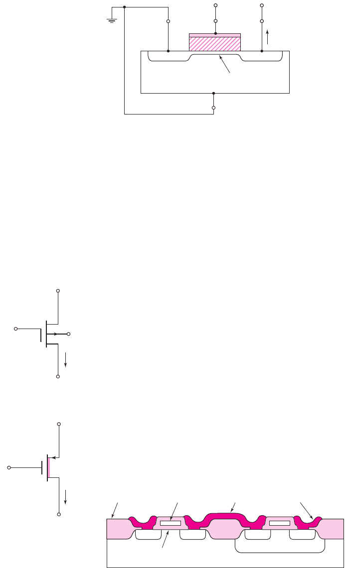
Complementary MOSFETs
Complementary MOS (CMOS) technology uses both n-channel and p-channel
devices in the same circuit. Figure 3.19 shows the cross section of n-channel and
p-channel devices fabricated on the same chip. CMOS circuits, in general, are more
complicated to fabricate than circuits using entirely NMOS or PMOS devices. Yet, as
we will see in later chapters, CMOS circuits have great advantages over just NMOS
or PMOS circuits.
nea80644_ch03_125-204.qxd 06/08/2009 08:37 PM Page 140 F506 Hard disk:Desktop Folder:MHDQ134-03:

Chapter 3 The Field-Effect Transistor 141
In order to fabricate n-channel and p-channel devices that are electrically equiv-
alent, the magnitude of the threshold voltages must be equal, and the n-channel and
p-channel conduction parameters must be equal. Since, in general,
μ
n
, and
μ
p
are not
equal, the design of equivalent transistors involves adjusting the width-to-length
ratios of the transistors.
Summary of Transistor Operation
We have presented a first-order model of the operation of the MOS transistor. For an
n-channel enhancement-mode MOSFET, a positive gate-to-source voltage, greater
than the threshold voltage
V
TN
, must be applied to induce an electron inversion layer.
For
v
GS
> V
TN
, the device is turned on. For an n-channel depletion-mode device, a
channel between the source and drain exists even for
v
GS
= 0
. The threshold voltage
is negative, so that a negative value of
v
GS
is required to turn the device off.
For a p-channel device, all voltage polarities and current directions are reversed
compared to the NMOS device. For the p-channel enhancement-mode transistor,
V
TP
< 0
and for the depletion-mode PMOS transistor,
V
TP
> 0
.
Table 3.1 lists the first-order equations that describe the i–
v
relationships in
MOS devices. We note that
K
n
and
K
p
are positive values and that the drain current
i
D
is positive into the drain for the NMOS device and positive out of the drain for the
PMOS device.
3.1.8
Table 3.1 Summary of the MOSFET current–voltage relationships
NMOS PMOS
Nonsaturation region (
v
DS
<v
DS
(sat)) Nonsaturation region (
v
SD
<v
SD
(sat))
i
D
= K
n
[2(v
GS
− V
TN
)v
DS
−v
2
DS
] i
D
= K
p
[2(v
SG
+ V
TP
)v
SD
−v
2
SD
]
Saturation region (
v
DS
>v
DS
(sat)) Saturation region
(v
SD
>v
SD
(sat))
i
D
= K
n
(v
GS
− V
TN
)
2
i
D
= K
p
(v
SG
+ V
TP
)
2
Transition point Transition point
v
DS
(sat) = v
GS
− V
TN
v
SD
(sat) = v
SG
+ V
TP
Enhancement mode Enhancement mode
V
TN
> 0 V
TP
< 0
Depletion mode Depletion mode
V
TN
< 0 V
TP
> 0
Short-Channel Effects
The current–voltage relations given by Equations (3.2(a)) and (3.2(b)) for the n-channel
device and Equations (3.4(a)) and (3.4(b)) for the p-channel device are the ideal
relations for long-channel devices. A long-channel device is generally one whose
channel length is greater than 2
μ
m. In this device, the horizontal electric field in the
channel induced by the drain voltage and the vertical electric field induced by the
gate voltage can be treated independently. However, the channel length of present-
day devices is on the order of 0.2
μ
m or less.
There are several effects in these short-channel devices that influence and
change the long-channel current–voltage characteristics. One such effect is a variation
3.1.9
nea80644_ch03_125-204.qxd 06/08/2009 08:37 PM Page 141 F506 Hard disk:Desktop Folder:MHDQ134-03:

142 Part 1 Semiconductor Devices and Basic Applications
in threshold voltage. The value of threshold voltage is a function of the channel
length. This variation must be considered in the design and fabrication of these
devices. The threshold voltage also becomes a function of the drain voltage. As the
drain voltage increases, the effective threshold voltage decreases. This effect also
influences the current–voltage characteristics.
The process conduction parameters,
k
n
and
k
p
, are directly related to the carrier
mobility. We have assumed that the carrier mobilities and corresponding process
conduction parameters are constant. However, the carrier mobility values are func-
tions of the vertical electric field in the inversion layer. As the gate voltage and verti-
cal electric field increase, the carrier mobility decreases. This result, again, directly
influences the current–voltage characteristics of the device.
Another effect that occurs in short-channel devices is velocity saturation. As the
horizontal electric field increases, the velocity of the carriers reaches a constant value
and will no longer increase with an increase in drain voltage. Velocity saturation will
lower the
V
DS
(sat)
voltage value. The drain current will reach its saturation value at
a smaller
V
DS
voltage. The drain current also becomes approximately a linear func-
tion of the gate voltage in the saturation region rather than the quadratic function of
gate voltage in the long-channel characteristics.
Although the analysis of modern MOSFET circuits must take into account these
short-channel effects, we will use the long-channel current–voltage relations in this
introductory text. We will still be able to obtain a good basic understanding of the op-
eration and characteristics of these devices, and we can still obtain a good basic un-
derstanding of the operation and characteristics of MOSFET circuits using the ideal
long-channel current–voltage relations.
Additional Nonideal
Current–Voltage Characteristics
The five nonideal effects in the current–voltage characteristics of MOS transistors
are: the finite output resistance in the saturation region, the body effect, subthreshold
conduction, breakdown effects, and temperature effects. This section will examine
each of these effects.
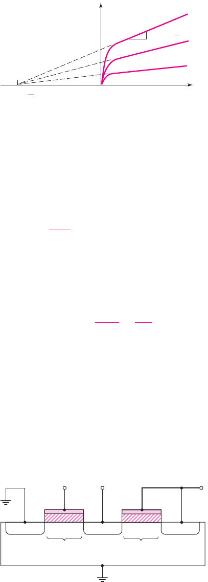
Finite Output Resistance
In the ideal case, when a MOSFET is biased in the saturation region, the drain
current i
D
is independent of drain-to-source voltage
v
DS
. However, in actual
MOSFET i
D
versus
v
DS
characteristics, a nonzero slope does exist beyond the sat-
uration point. For
v
DS
>v
DS
(sat)
, the actual point in the channel at which the in-
version charge goes to zero moves away from the drain terminal (see Figure
3.9(d)). The effective channel length decreases, producing the phenomenon called
channel length modulation.
An exaggerated view of the current–voltage characteristics is shown in Figure 3.20.
The curves can be extrapolated so that they intercept the voltage axis at a point
v
DS
=−V
A
. The voltage
V
A
is usually defined as a positive quantity. The slope of the
curve in the saturation region can be described by expressing the
i
D
versus
v
DS
char-
acteristic in the form, for an n-channel device,
i
D
= K
n
[(v
GS
− V
TN
)
2
(1 + λv
DS
)]
(3.7)
where
λ
is a positive quantity called the channel-length modulation parameter.
3.1.10
nea80644_ch03_125-204.qxd 06/08/2009 08:37 PM Page 142 F506 Hard disk:Desktop Folder:MHDQ134-03:
Chapter 3 The Field-Effect Transistor 143
The parameters
λ
and
V
A
are related. From Equation (3.7), we have
(1 + λv
DS
) = 0
at the extrapolated point where
i
D
= 0
. At this point,
v
DS
=−V
A
,
which means that
V
A
= 1/λ
.
The output resistance due to the channel length modulation is defined as
r
o
=
∂i
D
∂v
DS
−1
v
GS
=const.
(3.8)
From Equation (3.7), the output resistance, evaluated at the Q-point, is
r
o
= [λK
n
(V
GSQ
− V
TN
)
2
]
−1
(3.9(a))
or
r
o
∼
=
[λ I
DQ
]
−1
=
1
λ I
DQ
=
V
A
I
DQ
(3.9(b))
The output resistance
r
o
is also a factor in the small-signal equivalent circuit of the
MOSFET, which is discussed in the next chapter.
Body Effect
Up to this point, we have assumed that the substrate, or body, is connected to the
source. For this bias condition, the threshold voltage is a constant.
In integrated circuits, however, the substrates of all n-channel MOSFETs are
usually common and are tied to the most negative potential in the circuit. An exam-
ple of two n-channel MOSFETs in series is shown in Figure 3.21. The p-type
i
D
v
D
S
0
Slope =
1
r
o
–V
A
= –
λ
1
Figure 3.20 Family of
i
D
versus
v
DS
curves showing the effect of channel length
modulation producing a finite output resistance
p-substrate
V
O
V
DD
V
I
S
1
S
2
D
1
D
2
M
1
n
+
n
+
n
+
M
2
Figure 3.21 Two n-channel MOSFETs fabricated in series in the same substrate. The source
terminal,
S
2
, of the transistor
M
2
is more than likely not at ground potential.
nea80644_ch03_125-204.qxd 06/08/2009 08:37 PM Page 143 F506 Hard disk:Desktop Folder:MHDQ134-03:
144 Part 1 Semiconductor Devices and Basic Applications
substrate is common to the two transistors, and the drain of
M
1
is common to
the source of
M
2
. When the two transistors are conducting, there is a nonzero drain-
to-source voltage on
M
1
, which means that the source of
M
2
is not at the same
potential as the substrate. These bias conditions mean that a zero or reverse-bias
voltage exists across the source–substrate pn junction, and a change in the source–
substrate junction voltage changes the threshold voltage. This is called the body
effect. The same situation exists in p-channel devices.
For example, consider the n-channel device shown in Figure 3.22. To maintain a
zero- or reverse-biased source–substrate pn junction, we must have
v
SB
≥ 0
. The
threshold voltage for this condition is given by
V
TN
= V
TNO
+γ
2φ
f
+v
SB
−
2φ
f
(3.10)
where
V
TNO
is the threshold voltage for
v
SB
= 0
;
γ
, called the bulk threshold or
body-effect parameter, is related to device properties, and is typically on the order
of 0.5 V
1/2
; and
φ
f
is a semiconductor parameter, typically on the order of 0.35 V,
and is a function of the semiconductor doping. We see from Equation (3.10) that the
threshold voltage in n-channel devices increases due to this body effect.
The body effect can cause a degradation in circuit performance because of the
changing threshold voltage. However, we will generally neglect the body effect in
our circuit analyses, for simplicity.
Subthreshold Conduction
If we consider the ideal current-voltage relationship for the n-channel MOSFET
biased in the saturation region, we have, from Equation (3.2(b)),
i
D
= K
n
(v
GS
− V
TN
)
2
Taking the square root of both sides of the equation, we obtain
i
D
=
K
n
(v
GS
− V
TN
)
(3.11)
From Equation (3.11), we see that
√
i
d
is a linear function of
v
GS
. Figure 3.23 shows
a plot of this ideal relationship.
Also plotted in Figure 3.23 are experimental results, which show that when
v
GS
is slightly less than
V
TN
, the drain current is not zero, as previously assumed. This
current is called the subthreshold current. The effect may not be significant for a
single device, but if thousands or millions of devices on an integrated circuit are
biased just slightly below the threshold voltage, the power supply current will not
be zero but may contribute to significant power dissipation in the integrated circuit.
One example of this is a dynamic random access memory (DRAM), as we will see in
Chapter 16.
In this text, for simplicity we will not specifically consider the subthreshold
current. However, when a MOSFET in a circuit is to be turned off, the “proper”
design of the circuit must involve biasing the device at least a few tenths of a volt
below the threshold voltage to achieve “true” cutoff.
Breakdown Effects
Several possible breakdown effects may occur in a MOSFET. The drain-to-substrate
pn junction may break down if the applied drain voltage is too high and avalanche
multiplication occurs. This breakdown is the same reverse-biased pn junction break-
down discussed in Chapter 1 in Section 1.2.5.
+
+
–
–
v
SB
v
GS
G
B
D
S
Figure 3.22 An n-channel
enhancement-mode
MOSFET with a substrate
voltage
i
D
V
TN
v
G
S
Experimental
Ideal
Figure 3.23 Plot of
√
i
D
versus
v
GS
for a MOSFET
biased in the saturation
region showing subthreshold
conduction. Experimentally, a
subthreshold current exists
even for
v
GS
< V
TN
.
nea80644_ch03_125-204.qxd 06/08/2009 08:37 PM Page 144 F506 Hard disk:Desktop Folder:MHDQ134-03:

Chapter 3 The Field-Effect Transistor 145
As the size of the device becomes smaller, another breakdown mechanism,
called punch-through, may become significant. Punch-through occurs when the
drain voltage is large enough for the depletion region around the drain to extend com-
pletely through the channel to the source terminal. This effect also causes the drain
current to increase rapidly with only a small increase in drain voltage.
A third breakdown mechanism is called near-avalanche or snapback break-
down. This breakdown process is due to second-order effects within the MOSFET.
The source-substrate-drain structure is equivalent to that of a bipolar transistor. As
the device size shrinks, we may begin to see a parasitic bipolar transistor action with
increases in the drain voltage. This parasitic action enhances the breakdown effect.
If the electric field in the oxide becomes large enough, breakdown can also occur
in the oxide, which can lead to catastrophic failure. In silicon dioxide, the electric
field at breakdown is on the order of
6 × 10
6
V/cm
, which, to a first approximation,
is given by
E
ox
= V
G
/t
ox
. A gate voltage of approximately 30 V would produce
breakdown in an oxide with a thickness of
t
ox
= 500
˚
A
. However, a safety margin of
a factor of 3 is common, which means that the maximum safe gate voltage for
t
ox
= 500
˚
A
would be 10 V. A safety margin is necessary since there may be defects
in the oxide that lower the breakdown field. We must also keep in mind that the input
impedance at the gate is very high, and a small amount of static charge accumulating
on the gate can cause the breakdown voltage to be exceeded. To prevent the accumu-
lation of static charge on the gate capacitance of a MOSFET, a gate protection
device, such as a reverse-biased diode, is usually included at the input of a MOS
integrated circuit.
Temperature Effects
Both the threshold voltage
V
TN
and conduction parameter
K
n
are functions of tem-
perature. The magnitude of the threshold voltage decreases with temperature, which
means that the drain current increases with temperature at a given
V
GS
. However, the
conduction parameter is a direct function of the inversion carrier mobility, which de-
creases as the temperature increases. Since the temperature dependence of mobility is
larger than that of the threshold voltage, the net effect of increasing temperature is a de-
crease in drain current at a given
V
GS
. This particular result provides a negative feed-
back condition in power MOSFETs. A decreasing value of
K
n
inherently limits the
channel current and provides stability for a power MOSFET.
Test Your Understanding
TYU 3.1 (a) An n-channel enhancement-mode MOSFET has a threshold voltage of
V
TN
= 1.2V
and an applied gate-to-source voltage of
v
GS
= 2V
. Determine the
region of operation when: (i)
v
DS
= 0.4V
; (ii)
v
DS
= 1V
; and (iii)
v
DS
= 5V
.
(b) Repeat part (a) for an n-channel depletion-mode MOSFET with a threshold
voltage of
V
TN
=−1.2V
. (Ans. (a) (i) nonsaturation, (ii) saturation, (iii) saturation;
(b) (i) nonsaturation, (ii) nonsaturation, (iii) saturation)
TYU 3.2 The NMOS devices described in Exercise TYU 3.1 have parameters
W = 20 μm
,
L = 0.8 μm
,
t
ox
= 200
˚
A
,
μ
n
= 500 cm
2
/V–s
, and
λ = 0
. (a) Calcu-
late the conduction parameter
K
n
for each device. (b) Calculate the drain current for
each bias condition listed in Exercise TYU 3.1. (Ans. (a)
K
n
= 1.08 mA/V
2
;
(b)
i
D
= 0.518
mA, 0.691 mA, and 0.691 mA;
i
D
= 2.59
mA, 5.83 mA, and 11.1 mA)
nea80644_ch03_125-204.qxd 06/08/2009 08:37 PM Page 145 F506 Hard disk:Desktop Folder:MHDQ134-03:

146 Part 1 Semiconductor Devices and Basic Applications
TYU 3.3 (a) A p-channel enhancement-mode MOSFET has a threshold voltage of
V
TP
=−1.2V
and an applied source-to-gate voltage of
v
SG
= 2V
. Determine
the region of operation when (i)
v
SD
= 0.4V,
(ii)
v
SD
= 1V
, and (iii)
v
SD
= 5V
.
(b) Repeat part (a) for a p-channel depletion-mode MOSFET with a threshold volt-
age of
V
TP
=+1.2V
. (Ans. (a) (i) nonsaturation, (ii) saturation, (iii) saturation;
(b) (i) nonsaturation, (ii) nonsaturation, (iii) saturation)
TYU 3.4 The PMOS devices described in Exercise TYU 3.3 have parameters
W = 10 μm
,
L = 0.8 μm
,
t
ox
= 200
˚
A
,
μ
p
= 300 cm
2
/V
–s, and
λ = 0.
(a) Calculate
the conduction parameter
K
p
for each device. (b) Calculate the drain current for each
bias condition listed in Exercise TYU 3.3. (Ans. (a)
K
p
= 0.324 mA/V
2
;
(b)
i
D
= 0.156 mA,
0.207 mA; and 0.207 mA;
i
D
= 0.778 mA,
1.75 mA, and 3.32
mA)
TYU 3.5 The parameters of an NMOS enhancement-mode device are
V
TN
= 0.25 V
and
K
n
= 10 μ A/V
2
. The device is biased at
v
GS
= 0.5V
. Calculate the drain current
when (i)
v
DS
= 0.5V
and (ii)
v
DS
= 1.2V
for (a)
λ = 0
and (b)
λ = 0.03 V
−1
. (c) Cal-
culate the output resistance
r
o
for parts (a) and (b). (Ans. (a) (i) and (ii)
i
D
= 0.625 μA
;
(b) (i)
i
D
= 0.6344 μA
, (ii)
i
D
= 0.6475 μA
; (c) (i)
r
o
=∞
, (ii)
r
o
= 53.3M
).
TYU 3.6 An NMOS transistor has parameters
V
TNO
= 0.4V
,
γ = 0.15 V
1/2
, and
φ
f
= 0.35 V
. Calculate the threshold voltage when (a)
v
SB
= 0
, (b)
v
SB
= 0.5V
,
and (c)
v
SB
= 1.5V
. (Ans. (a) 0.4 V, (b) 0.439 V, (c) 0.497 V)
3.2 MOSFET DC CIRCUIT ANALYSIS
Objective: • Understand and become familiar with the dc analysis
and design techniques of MOSFET circuits.
In the last section, we considered the basic MOSFET characteristics and properties.
We now start analyzing and designing the dc biasing of MOS transistor circuits.
A primary purpose of the rest of the chapter is to continue to become familiar and
comfortable with the MOS transistor and MOSFET circuits. The dc biasing of
MOSFETs, the focus of this chapter, is an important part of the design of amplifiers.
MOSFET amplifier design is the focus of the next chapter.
In most of the circuits presented in this chapter, resistors are used in conjunction
with the MOS transistors. In a real MOSFET integrated circuit, however, the resistors
are generally replaced by other MOSFETs, so the circuit is composed entirely of MOS
devices. In general, a MOSFET device requires a smaller area than a resistor. As we
go through the chapter, we will begin to see how this is accomplished and as we fin-
ish the text, we will indeed analyze and design circuits containing only MOSFETs.
In the dc analysis of MOSFET circuits, we can use the ideal current–voltage
equations listed in Table 3.l in Section 3.1.
Common-Source Circuit
One of the basic MOSFET circuit configurations is called the common-source
circuit. Figure 3.24 shows one example of this type of circuit using an n-channel
3.2.1
nea80644_ch03_125-204.qxd 06/08/2009 08:37 PM Page 146 F506 Hard disk:Desktop Folder:MHDQ134-03:

Chapter 3 The Field-Effect Transistor 147
enhancement-mode MOSFET. The source terminal is at ground potential and is
common to both the input and output portions of the circuit. The coupling capacitor
C
C
acts as an open circuit to dc but it allows the signal voltage to be coupled to the
gate of the MOSFET.
The dc equivalent circuit is shown in Figure 3.25(a). In the following dc ana-
lyses, we again use the notation for dc currents and voltages. Since the gate current
into the transistor is zero, the voltage at the gate is given by a voltage divider, which
can be written as
V
G
= V
GS
=
R
2
R
1
+ R
2
V
DD
(3.12)
Assuming that the gate-to-source voltage given by Equation (3.12) is greater
than
V
TN
, and that the transistor is biased in the saturation region, the drain current is
I
D
= K
n
(V
GS
− V
TN
)
2
(3.13)
The drain-to-source voltage is
V
DS
= V
DD
− I
D
R
D
(3.14)
If
V
DS
> V
DS
(sat) = V
GS
− V
TN
, then the transistor is biased in the saturation
region, as we initially assumed, and our analysis is correct. If
V
DS
< V
DS
(sat)
, then
the transistor is biased in the nonsaturation region, and the drain current is given by
the more complicated characteristic Equation (3.2(a)).
The power dissipated in the transistor, since there is no gate current, is simply
given by
P
T
= I
D
V
DS
(3.15)
EXAMPLE 3.3
Objective: Calculate the drain current and drain-to-source voltage of a common-
source circuit with an n-channel enhancement-mode MOSFET. Find the power
dissipated in the transistor.
For the circuit shown in Figure 3.25(a), assume that
R
1
= 30 k
,
R
2
= 20 k
,
R
D
= 20 k
,
V
DD
= 5V
,
V
TN
= 1V
, and
K
n
= 0.1mA/V
2
.
R
1
V
DD
R
2
R
D
v
O
v
i
i
D
+
+
–
–
v
DS
v
GS
v
G
C
C
+
–
Figure 3.24 An NMOS common-
source circuit
V
DD
V
G
R
D
R
1
R
2
+
+
0
–
–
V
DS
V
GS
I
D
V
DD
= 5 V
R
D
= 20 kΩ
R
1
= 30 kΩ
R
2
= 20 kΩ
+
+
–
–
V
DS
= 5 – (0.1)(20)
= 3 V
V
GS
= 2 V
I
D
= 0.1 mA
V
G
= (5)
()
20
50
= 2 V
(a) (b)
Figure 3.25 (a) The dc equivalent circuit of the NMOS common-source
circuit and (b) the NMOS circuit for Example 3.3, showing current and
voltage values
nea80644_ch03_125-204.qxd 06/08/2009 08:37 PM Page 147 F506 Hard disk:Desktop Folder:MHDQ134-03: