Neamen D. Microelectronics: Circuit Analysis and Design
Подождите немного. Документ загружается.

128 Part 1 Semiconductor Devices and Basic Applications
n-type
–
+
––––
V
Induced positive space-charge region
E
n-type
E
–
+
––––––
++++++
V
Hole inversion layer
E
(a)
n-type
+
–
++++++
––––––
V
Electron
accumulation
layer
E
(b) (c)
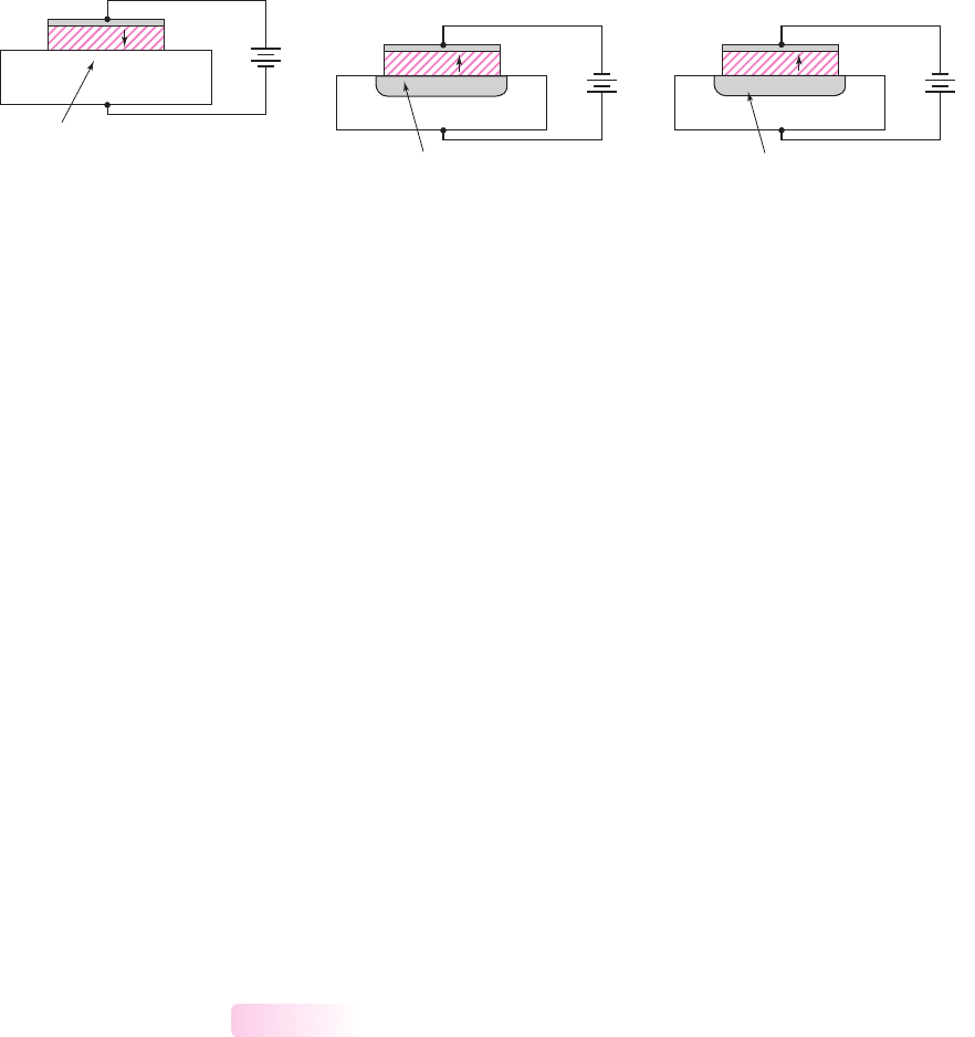
Figure 3.4 The MOS capacitor with n-type substrate: (a) effect of a positive gate bias and
the formation of an electron accumulation layer, (b) the MOS capacitor with an induced
space-charge region due to a moderate negative gate bias, and (c) the MOS capacitor with an
induced space-charge region and hole inversion layer due to a larger negative gate bias
When a larger positive voltage is applied to the gate, the magnitude of the
induced electric field increases. Minority carrier electrons are attracted to the oxide-
semiconductor interface, as shown in Figure 3.3(c). This region of minority carrier
electrons is called an electron inversion layer. The magnitude of the charge in the
inversion layer is a function of the applied gate voltage.
The same basic charge distributions can be obtained in a MOS capacitor with
an n-type semiconductor substrate. Figure 3.4(a) shows this MOS capacitor struc-
ture, with a positive voltage applied to the top gate terminal. A positive charge is
created on the top gate and an electric field is induced in the direction shown. In
this situation, an accumulation layer of electrons is induced in the n-type semi-
conductor.
Figure 3.4(b) shows the case when a negative voltage is applied to the gate ter-
minal. A positive space-charge region is induced in the n-type substrate by the
induced electric field. When a larger negative voltage is applied, a region of positive
charge is created at the oxide-semiconductor interface, as shown in Figure 3.4(c).
This region of minority carrier holes is called a hole inversion layer. The magnitude
of the positive charge in the inversion layer is a function of the applied gate voltage.
The term enhancement mode means that a voltage must be applied to the gate
to create an inversion layer. For the MOS capacitor with a p-type substrate, a positive
gate voltage must be applied to create the electron inversion layer; for the MOS
capacitor with an n-type substrate, a negative gate voltage must be applied to create
the hole inversion layer.
n-Channel Enhancement-Mode MOSFET
We will now apply the concepts of an inversion layer charge in a MOS capacitor to
create a transistor.
Transistor Structure
Figure 3.5(a) shows a simplified cross section of a MOS field-effect transistor. The
gate, oxide, and p-type substrate regions are the same as those of a MOS capacitor.
In addition, we now have two n-regions, called the source terminal and drain
terminal. The current in a MOSFET is the result of the flow of charge in the inver-
sion layer, also called the channel region, adjacent to the oxide–semiconductor
interface.
3.1.2
nea80644_ch03_125-204.qxd 06/08/2009 08:36 PM Page 128 F506 Hard disk:Desktop Folder:MHDQ134-03:
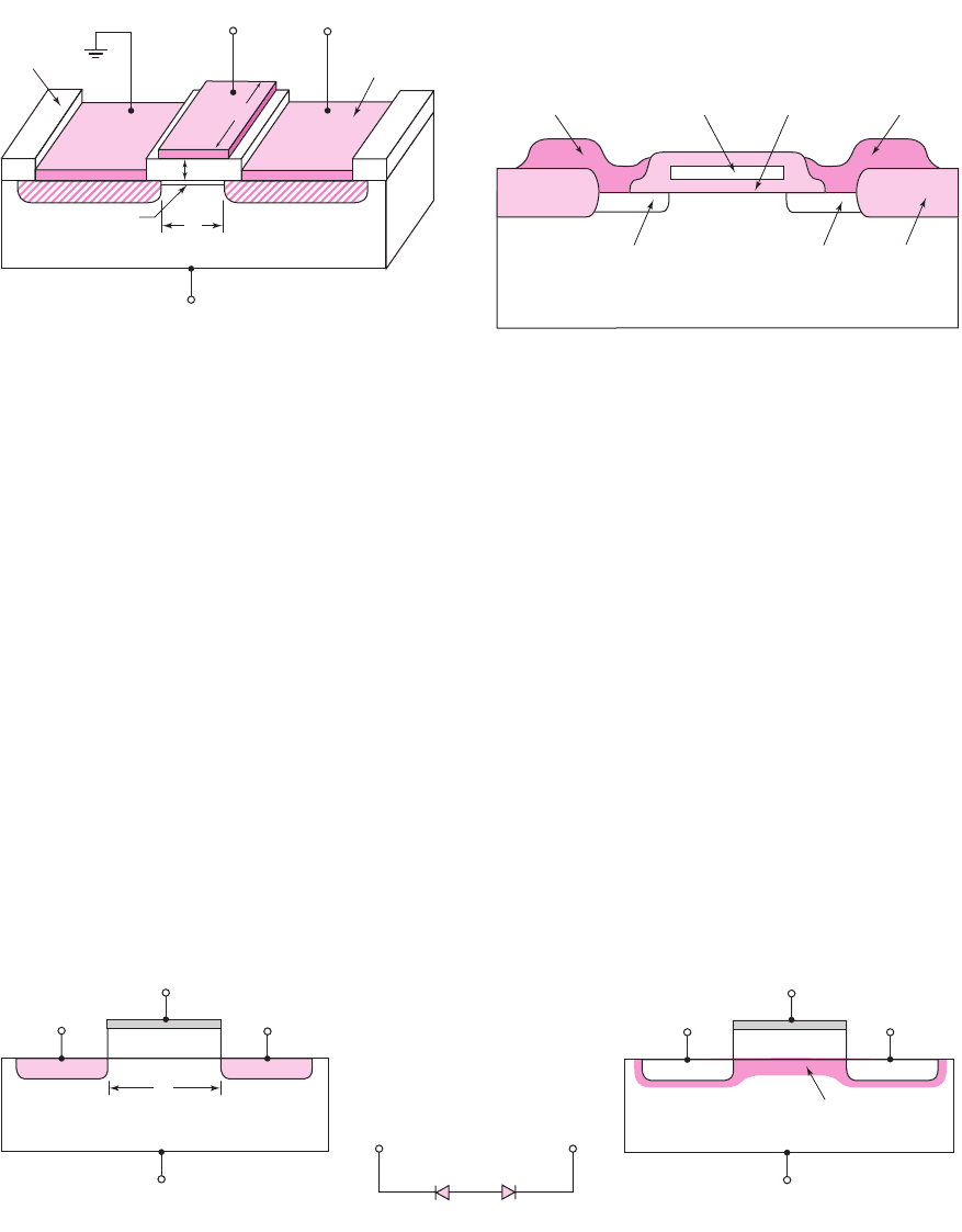
Chapter 3 The Field-Effect Transistor 129
p-substrate
Source Drain
Gate oxide
Field oxide
Source metal Drain metalPoly gate
n
+
n
+
(b)
Source
Metal
electrode
(Substrate bias)
Oxide
Channel
p-type
v
GS
v
DS
n
+
L
(a)
Gate
W
Source
Drain
t
ox
n
+
Figure 3.5 (a) Schematic diagram of an n-channel enhancement-mode MOSFET and (b) an
n-channel MOSFET, showing the field oxide and polysilicon gate
The channel length L and channel width W are defined on the figure. The chan-
nel length of a typical integrated circuit MOSFET is less than 1 μm (
10
−6
m), which
means that MOSFETs are small devices. The oxide thickness
t
ox
is typically on the
order of 400 angstroms, or less.
The diagram in Figure 3.5(a) is a simplified sketch of the basic structure of the
transistor. Figure 3.5(b) shows a more detailed cross section of a MOSFET fabricated
into an integrated circuit configuration. A thick oxide, called the field oxide, is
deposited outside the area in which the metal interconnect lines are formed. The gate
material is usually heavily doped polysilicon. Even though the actual structure of a
MOSFET may be fairly complex, the simplified diagram may be used to develop the
basic transistor characteristics.
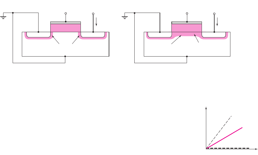
Basic Transistor Operation
With zero bias applied to the gate, the source and drain terminals are separated by the
p-region, as shown in Figure 3.6(a). This is equivalent to two back-to-back diodes, as
shown in Figure 3.6(b). The current in this case is essentially zero. If a large enough
positive gate voltage is applied, an electron inversion layer is created at the
oxide–semiconductor interface and this layer “connects” the n-source to the n-drain,
p-type
Gate (G)
Substrate or body (B)
Source (S)
Drain (D)
n
+
n
+
L
S
D
p
Electron
inversion layer
G
Substrate or body (B)
n
+
n
+
SD
–––––––
(a) (b) (c)
Figure 3.6 (a) Cross section of the n-channel MOSFET prior to the formation of an electron
inversion layer, (b) equivalent back-to-back diodes between source and drain when the
transistor is in cutoff, and (c) cross section after the formation of an electron inversion layer
nea80644_ch03_125-204.qxd 06/08/2009 08:36 PM Page 129 F506 Hard disk:Desktop Folder:MHDQ134-03:

130 Part 1 Semiconductor Devices and Basic Applications
2
The usual notation for threshold voltage is
V
T
. However, since we have defined the thermal voltage as
V
T
= kT/q
, we will use
V
TN
for the threshold voltage of the n-channel device.
3
The voltage notation
v
DS
and
v
GS
, with the dual subscript, denotes the voltage between the drain (D) and
source (S) and between the gate (G) and source (S), respectively. Implicit in the notation is that the first
subscript is positive with respect to the second subscript.
as shown in Figure 3.6(c). A current can then be generated between the source and
drain terminals. Since a voltage must be applied to the gate to create the inversion
charge, this transistor is called an enhancement-mode MOSFET. Also, since the
carriers in the inversion layer are electrons, this device is also called an n-channel
MOSFET (NMOS).
The source terminal supplies carriers that flow through the channel, and the
drain terminal allows the carriers to drain from the channel. For the n-channel
MOSFET, electrons flow from the source to the drain with an applied drain-to-source
voltage, which means the conventional current enters the drain and leaves the source.
The magnitude of the current is a function of the amount of charge in the inversion
layer, which in turn is a function of the applied gate voltage. Since the gate terminal
is separated from the channel by an oxide or insulator, there is no gate current.
Similarly, since the channel and substrate are separated by a space-charge region,
there is essentially no current through the substrate.
Ideal MOSFET Current–Voltage
Characteristics—NMOS Device
The threshold voltage of the n-channel MOSFET, denoted as
V
TN
, is defined
2
as the
applied gate voltage needed to create an inversion charge in which the density is
equal to the concentration of majority carriers in the semiconductor substrate. In
simple terms, we can think of the threshold voltage as the gate voltage required to
“turn on” the transistor.
For the n-channel enhancement-mode MOSFET, the threshold voltage is posi-
tive because a positive gate voltage is required to create the inversion charge. If the
gate voltage is less than the threshold voltage, the current in the device is essentially
zero. If the gate voltage is greater than the threshold voltage, a drain-to-source
current is generated as the drain-to-source voltage is applied. The gate and drain
voltages are measured with respect to the source.
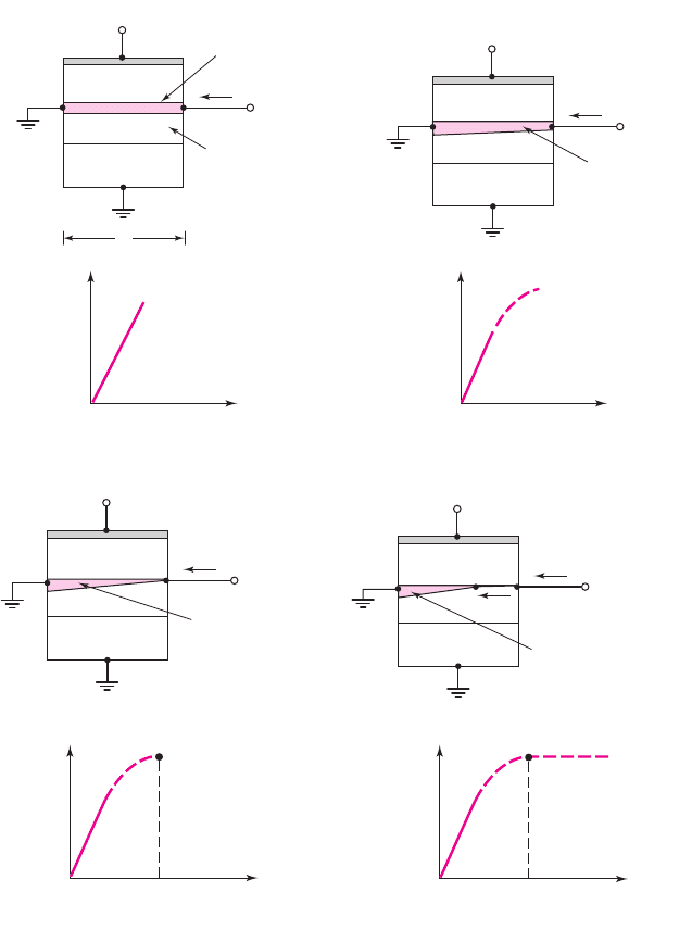
Figure 3.7(a) shows an n-channel enhancement-mode MOSFET with the source
and substrate terminals connected to ground. The gate-to-source voltage is less than
the threshold voltage, and there is a small drain-to-source voltage. With this bias
configuration, there is no electron inversion layer, the drain-to-substrate pn junction
is reverse biased, and the drain current is zero (neglecting pn junction leakage
currents).
Figure 3.7(b) shows the same MOSFET with an applied gate voltage greater
than the threshold voltage. In this situation, an electron inversion layer is created and,
when a small drain voltage is applied, electrons in the inversion layer flow from the
source to the positive drain terminal. The conventional current enters the drain
terminal and leaves the source terminal. Note that a positive drain voltage creates a
reverse-biased drain-to-substrate pn junction, so current flows through the channel
region and not through a pn junction.
The i
D
versus
v
DS
characteristics
3
for small values of
v
DS
are shown in Fig-
ure 3.8. When
v
GS
< V
TN
, the drain current is zero. When
v
GS
is greater than
V
TN
,
3.1.3
nea80644_ch03_125-204.qxd 06/08/2009 08:36 PM Page 130 F506 Hard disk:Desktop Folder:MHDQ134-03:
Chapter 3 The Field-Effect Transistor 131
p
Space-
charge regions
G
S
D
n
+
n
+
v
GS
< V
TN
+v
DS
i
D
= 0
p
Induced electron
inversion layer
Space-
charge regions
G
S
D
n
+
n
+
v
GS
> V
TN
+v
DS
i
D
–––––––
(a) (b)
Figure 3.7 The n-channel enhancement-mode MOSFET (a) with an applied gate voltage
v
GS
< V
TN
, and (b) with an applied gate voltage
v
GS
> V
TN
v
GS2
> v
GS1
v
GS1
> V
TN
v
GS
< V
TN
v
D
S
i
D
Figure 3.8 Plot of
i
D
versus
v
DS
characteristic for small
values of
v
DS
at three
v
GS
voltages
the channel inversion charge is formed and the drain current increases with
v
DS
.
Then, with a larger gate voltage, a larger inversion charge density is created, and the
drain current is greater for a given value of
v
DS
.
Figure 3.9(a) shows the basic MOS structure for
v
GS
> V
TN
and a small applied
v
DS
. In the figure, the thickness of the inversion channel layer qualitatively indicates
the relative charge density, which for this case is essentially constant along the entire
channel length. The corresponding i
D
versus
v
DS
curve is also shown in the figure.
Figure 3.9(b) shows the situation when
v
DS
increases. As the drain voltage
increases, the voltage drop across the oxide near the drain terminal decreases, which
means that the induced inversion charge density near the drain also decreases. The in-
cremental conductance of the channel at the drain then decreases, which causes the
slope of the i
D
versus
v
DS
curve to decrease. This effect is shown in the i
D
versus
v
DS
curve in the figure.
As
v
DS
increases to the point where the potential difference,
v
GS
−v
DS
, across
the oxide at the drain terminal is equal to
V
TN
, the induced inversion charge density
at the drain terminal is zero. This effect is shown schematically in Figure 3.9(c). For
this condition, the incremental channel conductance at the drain is zero, which means
that the slope of the i
D
versus
v
DS
curve is zero. We can write
v
GS
−v
DS
(sat) = V
TN
(3.1(a))
or
v
DS
(sat) = v
GS
− V
TN
(3.1(b))
where
v
DS
(sat)
is the drain-to-source voltage that produces zero inversion charge
density at the drain terminal.
When
v
DS
becomes larger than
v
DS
(sat)
, the point in the channel at which the
inversion charge is just zero moves toward the source terminal. In this case, electrons
enter the channel at the source, travel through the channel toward the drain, and then,
at the point where the charge goes to zero, are injected into the space-charge region,
where they are swept by the E-field to the drain contact. In the ideal MOSFET, the
drain current is constant for
v
DS
>v
DS
(sat)
. This region of the i
D
versus
v
DS
char-
acteristic is referred to as the saturation region, which is shown in Figure 3.9(d).
As the applied gate-to-source voltage changes, the i
D
versus
v
DS
curve changes.
In Figure 3.8, we saw that the initial slope of i
D
versus
v
DS
increases as
v
GS
increases.
Also, Equation (3.1(b)) shows that
v
DS
(sat)
is a function of
v
GS
. Therefore, we can
nea80644_ch03_125-204.qxd 06/08/2009 08:36 PM Page 131 F506 Hard disk:Desktop Folder:MHDQ134-03:
132 Part 1 Semiconductor Devices and Basic Applications
generate the family of curves for this n-channel enhancement mode MOSFET as
shown in Figure 3.10.
Although the derivation of the current–voltage characteristics of the MOSFET
is beyond the scope of this text, we can define the relationships. The region for
which
v
DS
<v
DS
(sat)
is known as the nonsaturation or triode region. The ideal
current–voltage characteristics in this region are described by the equation
i
D
= K
n
2(v
GS
− V
TN
)v
DS
−v
2
DS
(3.2(a))
(a) (b)
(c) (d)
i
D
v
DS
i
D
v
DS
i
D
v
DS
v
DS
(sat)
i
D
v
DS
v
DS
(sat)
Saturation
region
v
GS1
> V
TN
v
DS
i
D
Channel
inversion
charge
Depletion
region
p-type
S
Oxide
L
v
GS1
v
DS
i
D
Channel
inversion
charge
p-type
S
Oxide
v
GS1
v
DS
(sat)
i
D
Channel
inversion
charge
p-type
S
Oxide
v
GS1
v
DS
> v
DS
(sat)
v
DS
(sat)
i
D
Channel
inversion
charge
p-type
S
E-field depletion region
Oxide
Figure 3.9 Cross section and
i
D
versus
v
DS
curve for an n-channel enhancement-mode
MOSFET when
v
GS
> V
TN
for (a) a small
v
DS
value, (b) a larger
v
DS
value but for
v
DS
<v
DS
(sat)
, (c)
v
DS
= v
DS
(sat), and (d)
v
DS
>v
DS
(sat)
nea80644_ch03_125-204.qxd 06/08/2009 08:36 PM Page 132 F506 Hard disk:Desktop Folder:MHDQ134-03:
Chapter 3 The Field-Effect Transistor 133
v
DS
v
GS1
> V
TN
> 0
v
GS2
> v
GS1
v
GS3
> v
GS2
v
GS4
> v
GS3
v
GS5
> v
GS4
v
DS
(sat) = v
GS
– V
TN
Saturation region
v
DS
> v
DS
(sat)
Nonsaturation
region,
v
DS
< v
DS
(sat)
i
D
Figure 3.10 Family of i
D
versus
v
DS
curves for an n-channel enhancement-mode MOSFET.
Note that the
v
DS
(sat)
voltage is a single point on each of the curves. This point denotes the
transition between the nonsaturation region and the saturation region
In the saturation region, the ideal current–voltage characteristics for
v
GS
> V
TN
are
described by the equation
i
D
= K
n
(v
GS
− V
TN
)
2
(3.2(b))
In the saturation region, since the ideal drain current is independent of the drain-to-
source voltage, the incremental or small-signal resistance is infinite. We see that
r
0
= v
DS
/i
D
|
v
GS
=const.
=∞
The parameter K
n
is sometimes called the transconduction parameter for the
n-channel device. However, this term is not to be confused with the small-signal
transconductance parameter introduced in the next chapter. For simplicity, we will
refer to this parameter as the conduction parameter, which for an n-channel device
is given by
K
n
=
Wμ
n
C
ox
2L
(3.3(a))
where C
ox
is the oxide capacitance per unit area. The capacitance is given by
C
ox
=
ox
/t
ox
where t
ox
is the oxide thickness and
ox
is the oxide permittivity. For silicon devices,
ox
= (3.9)(8.85 ×10
−14
)
F/cm. The parameter
μ
n
is the mobility of the electrons
in the inversion layer. The channel width W and channel length L were shown in
Figure 3.5(a).
As Equation (3.3(a)) indicates, the conduction parameter is a function of both
electrical and geometric parameters. The oxide capacitance and carrier mobility are
essentially constants for a given fabrication technology. However, the geometry, or
width-to-length ratio W/L, is a variable in the design of MOSFETs that is used to
produce specific current–voltage characteristics in MOSFET circuits.
We can rewrite the conduction parameter in the form
K
n
=
k
n
2
·
W
L
(3.3(b))
nea80644_ch03_125-204.qxd 06/08/2009 08:37 PM Page 133 F506 Hard disk:Desktop Folder:MHDQ134-03:

134 Part 1 Semiconductor Devices and Basic Applications
where
k
n
= μ
n
C
ox
and is called the process conduction parameter. Normally,
k
n
is considered to be a constant for a given fabrication technology, so Equation
(3.3(b)) indicates that the width-to-length ratio W/L is the transistor design
variable.
EXAMPLE 3.1
Objective: Calculate the current in an n-channel MOSFET.
Consider an n-channel enhancement-mode MOSFET with the following para-
meters:
V
TN
= 0.4V, W = 20 μm
,
L = 0.8 μm
,
μ
n
= 650 cm
2
/V–s, t
ox
= 200
Å,
and
ox
= (3.9)(8.85 ×10
−14
)
F/cm. Determine the current when the transistor is bi-
ased in the saturation region for (a)
v
GS
= 0.8V
and (b)
v
GS
= 1.6V
.
Solution: The conduction parameter is determined by Equation (3.3(a)). First,
consider the units involved in this equation, as follows:
K
n
=
W(cm) · μ
n
cm
2
V–s
ox
F
cm
2L(cm) · t
ox
(cm)
=
F
V–s
=
(C/V)
V–s
=
A
V
2
The value of the conduction parameter is therefore
K
n
=
Wμ
n
ox
2Lt
ox
=
(20 × 10
−4
)(650)(3.9)(8.85 ×10
−14
)
2(0.8 × 10
−4
)(200 × 10
−8
)
or
K
n
= 1.40 mA/V
2
From Equation (3.2(b)), we find:
(a) For
v
GS
= 0.8V
,
i
D
= K
n
(v
GS
− V
TN
)
2
= (1.40)(0.8 −0.4)
2
= 0.224 mA
(b) For
v
GS
= 1.6V
,
i
D
= (1.40)(1.6 −0.4)
2
= 2.02 mA
Comment: The current capability of a transistor can be increased by increasing the
conduction parameter. For a given fabrication technology,
K
n
is adjusted by varying
the transistor width W.
EXERCISE PROBLEM
Ex 3.1: An NMOS transistor with
V
TN
= 1
V has a drain current
i
D
= 0.8
mA
when
v
GS
= 3
V and
v
DS
= 4.5
V. Calculate the drain current when: (a)
v
GS
= 2
V,
v
DS
= 4.5
V; and (b)
v
GS
= 3
V,
v
DS
= 1
V. (Ans. (a) 0.2 mA (b) 0.6 mA)
p-Channel Enhancement-Mode MOSFET
The complementary device of the n-channel enhancement-mode MOSFET is the
p-channel enhancement-mode MOSFET.
3.1.4
nea80644_ch03_125-204.qxd 06/08/2009 08:37 PM Page 134 F506 Hard disk:Desktop Folder:MHDQ134-03:
Chapter 3 The Field-Effect Transistor 135
n-type
Body
L
GateSource
Drain
p
+
p
+
v
SD
+–
v
SG
+–
i
D
t
ox
W
Figure 3.11 Cross section of p-channel enhancement-mode MOSFET. The device is cut off
for
v
SG
= 0
. The dimension W extends into the plane of the page.
4
Using a different threshold voltage parameter for a PMOS device compared to the NMOS device is for
clarity only.
Transistor Structure
Figure 3.11 shows a simplified cross section of the p-channel enhancement-
mode transistor. The substrate is now n-type and the source and drain areas are
p-type. The channel length, channel width, and oxide thickness parameter definitions
are the same as those for the NMOS device shown in Figure 3.5(a).
Basic Transistor Operation
The operation of the p-channel device is the same as that of the n-channel device,
except the hole is the charge carrier rather than the electron. A negative gate bias is
required to induce an inversion layer of holes in the channel region directly under the
oxide. The threshold voltage for the p-channel device is denoted as
V
TP
.
4
Since the
threshold voltage is defined as the gate voltage required to induce the inversion layer,
then
V
TP
< 0
for the p-channel enhancement-mode device.
Once the inversion layer has been created, the p-type source region is the source
of the charge carrier so that holes flow from the source to the drain. A negative drain
voltage is therefore required to induce an electric field in the channel forcing the
holes to move from the source to the drain. The conventional current direction, then,
for the PMOS transistor is into the source and out of the drain. The conventional
current direction and voltage polarity for the PMOS device are reversed compared to
the NMOS device.
Note in Figure 3.11 the reversal of the voltage subscripts. For
v
SG
> 0
, the gate
voltage is negative with respect to that at the source. Similarly, for
v
SD
> 0
, the
drain voltage is negative with respect to that at the source.
Ideal MOSFET Current–Voltage
Characteristics—PMOS Device
The ideal current–voltage characteristics of the p-channel enhancement-mode device
are essentially the same as those shown in Figure 3.10, noting that the drain current
3.1.5
nea80644_ch03_125-204.qxd 06/08/2009 08:37 PM Page 135 F506 Hard disk:Desktop Folder:MHDQ134-03:

136 Part 1 Semiconductor Devices and Basic Applications
is out of the drain and
v
DS
is replaced by
v
SD
. The saturation point is given by
v
SD
(sat) = v
SG
+ V
TP
.
For the p-channel device biased in the nonsaturation region,
the current is given by
i
D
= K
p
2(v
SG
+ V
TP
)v
SD
−v
2
SD
(3.4(a))
In the saturation region, the current is given by
i
D
= K
p
(v
SG
+ V
TP
)
2
(3.4(b))
and the drain current exits the drain terminal. The parameter
K
p
is the conduction
parameter for the p-channel device and is given by
K
p
=
Wμ
p
C
ox
2L
(3.5(a))
where W, L, and
C
ox
are the channel width, length, and oxide capacitance per unit
area, as previously defined. The parameter
μ
p
is the mobility of holes in the hole
inversion layer. In general, the hole inversion layer mobility is less than the electron
inversion layer mobility.
We can also rewrite Equation (3.5(a)) in the form
K
p
=
k
p
2
·
W
L
(3.5(b))
where
k
p
= μ
p
C
ox
.
For a p-channel MOSFET biased in the saturation region, we have
v
SD
>v
SD
(sat) = v
SG
+ V
TP
(3.6)
EXAMPLE 3.2
Objective: Determine the source-to-drain voltage required to bias a p-channel
enhancement-mode MOSFET in the saturation region.
Consider an enhancement-mode p-channel MOSFET for which
K
p
= 0.2
mA/
V
2
,
V
TP
=−0.50
V, and
i
D
= 0.50
mA.
Solution: In the saturation region, the drain current is given by
i
D
= K
p
(v
SG
+ V
TP
)
2
or
0.50 = 0.2(v
SG
−0.50)
2
which yields
v
SG
= 2.08 V
To bias this p-channel MOSFET in the saturation region, the following must apply:
v
SD
>v
SD
(sat) = v
SG
+ V
TP
= 2.08 −0.5 = 1.58 V
Comment: Biasing a transistor in either the saturation or the nonsaturation region
depends on both the gate-to-source voltage and the drain-to-source voltage.
nea80644_ch03_125-204.qxd 06/08/2009 08:37 PM Page 136 F506 Hard disk:Desktop Folder:MHDQ134-03:
Chapter 3 The Field-Effect Transistor 137
+
+
–
–
v
DS
i
D
v
GS
B
G
D
S
+
+
–
–
v
DS
i
D
v
GS
G
D
S
(a) (b)
+
+
–
–
v
DS
i
D
v
GS
G
D
S
(c)
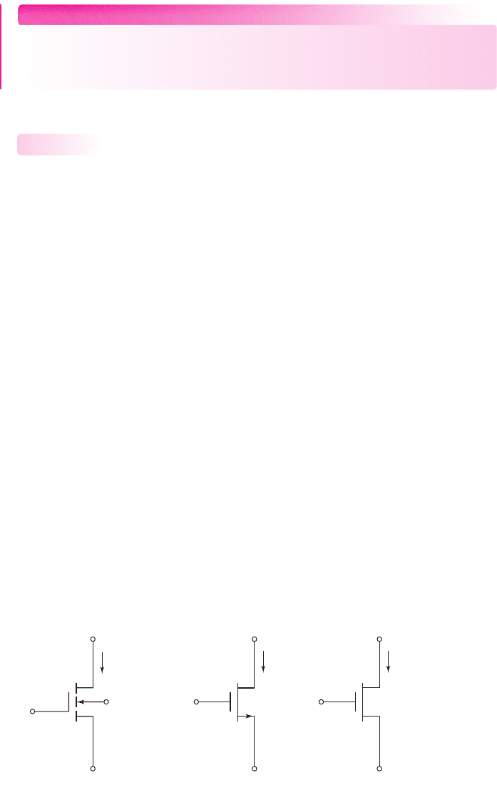
Figure 3.12 The n-channel enhancement-mode MOSFET: (a) conventional circuit symbol,
(b) circuit symbol that will be used in this text, and (c) a simplified circuit symbol used in
more advanced texts
EXERCISE PROBLEM
Ex 3.2: A PMOS device with
V
TP
=−1.2
V has a drain current
i
D
= 0.5
mA
when
v
SG
= 3
V and
v
SD
= 5
V. Calculate the drain current when (a)
v
SG
= 2
V,
v
SD
= 3
V; and (b)
v
SG
= 5
V,
v
SD
= 2
V. (Ans. (a) 0.0986 mA, (b) 1.72 mA)
Circuit Symbols and Conventions
The conventional circuit symbol for the n-channel enhancement-mode MOSFET is
shown in Figure 3.12(a). The vertical solid line denotes the gate electrode, the verti-
cal broken line denotes the channel (the broken line indicates the device is enhance-
ment mode), and the separation between the gate line and channel line denotes the
oxide that insulates the gate from the channel. The polarity of the pn junction
between the substrate and the channel is indicated by the arrowhead on the body or
substrate terminal. The direction of the arrowhead indicates the type of transistor,
which in this case is an n-channel device. This symbol shows the four-terminal struc-
ture of the MOSFET device.
In most applications in this text, we will implicitly assume that the source and
substrate terminals are connected together. Explicitly drawing the substrate terminal
for each transistor in a circuit becomes redundant and makes the circuits appear more
complex. Instead, we will use the circuit symbol for the n-channel MOSFET shown
in Figure 3.12(b). In this symbol, the arrowhead is on the source terminal and it
indicates the direction of current, which for the n-channel device is out of the source.
By including the arrowhead in the symbol, we do not need to explicitly indicate the
source and drain terminals. We will use this circuit symbol throughout the text except
in specific applications.
In more advanced texts and journal articles, the circuit symbol of the n-channel
MOSFET shown in Figure 3.12(c) is generally used. The gate terminal is obvious
and it is implicitly understood that the “top” terminal is the drain and the “bottom”
terminal is the source. The top terminal, in this case the drain, is usually at a more
positive voltage than the bottom terminal. In this introductory text, we will use the
symbol shown in Figure 3.12(b) for clarity.
3.1.6
nea80644_ch03_125-204.qxd 06/08/2009 08:37 PM Page 137 F506 Hard disk:Desktop Folder:MHDQ134-03: