Neamen D. Microelectronics: Circuit Analysis and Design
Подождите немного. Документ загружается.


158 Part 1 Semiconductor Devices and Basic Applications
If an enhancement-load device is connected in a circuit with another MOSFET
in the configuration shown in Figure 3.36, the circuit can be used as an amplifier or
as an inverter in a digital logic circuit. The load device, M
L
, is always biased in the
saturation region, and the transistor M
D
, called the driver transistor, can be biased
in either the saturation or nonsaturation region, depending on the value of the input
voltage. The next example addresses the dc analysis of this circuit for dc input volt-
ages to the gate of M
D
.
EXAMPLE 3.9
Objective: Determine the dc transistor currents and voltages in a circuit containing
an enhancement load device.
The transistors in the circuit shown in Figure 3.36 have parameters
V
TND
=
V
TNL
= 1V
,
K
nD
= 50 μA/V
2
, and
K
nL
= 10 μA/V
2
. Also assume
λ
nD
=
λ
nL
= 0
. (The subscript D applies to the driver transistor and the subscript L applies
to the load transistor.) Determine V
O
for
V
I
= 5V
and
V
I
= 1.5V
.
Solution:
(V
I
= 5V)
For an inverter circuit with a resistive load, when the input
voltage is large, the output voltage drops to a low value. Therefore, we assume that
the driver transistor is biased in the nonsaturation region since the drain-to-source
voltage will be small. The drain current in the load device is equal to the drain cur-
rent in the driver transistor. Writing these currents in generic form, we have
I
DD
= I
DL
or
K
nD
2(V
GSD
− V
TND
)V
DSD
− V
2
DSD
= K
nL
[V
GSL
− V
TNL
]
2
Since
V
GSD
= V
I
,
V
DSD
= V
O
, and
V
GSL
= V
DSL
= V
DD
− V
O
, then
K
nD
2(V
I
− V
TND
)V
O
− V
2
O
= K
nL
[V
DD
− V
O
− V
TNL
]
2
Substituting numbers, we find
(50)
2(5 − 1)V
O
− V
2
O
= (10)[5 − V
O
−1]
2
Figure 3.36 Circuit with enhancement-load device and NMOS driver
V
DD
= 5 V
V
O
M
D
V
I
M
L
I
DL
I
DD
Load
Drive
r
+
–
V
DSL
+
–
V
GSL
+
–
V
GSD
+
–
V
DSD
nea80644_ch03_125-204.qxd 06/08/2009 08:37 PM Page 158 F506 Hard disk:Desktop Folder:MHDQ134-03:

Chapter 3 The Field-Effect Transistor 159
Rearranging the terms provides
3V
2
O
−24V
O
+8 = 0
Using the quadratic formula, we obtain two possible solutions:
V
O
= 7.65 V or V
O
= 0.349 V
Since the output voltage cannot be greater than the supply voltage
V
DD
= 5V
, the
valid solution is
V
O
= 0.349 V
.
Also, since
V
DSD
= V
O
= 0.349 V < V
GSD
− V
TND
= 5 −1 = 4V
, the driver
M
D
is biased in the nonsaturation region, as initially assumed.
The current can be determined from
I
D
= K
nL
(V
GSL
− V
TNL
)
2
= K
nL
(V
DD
− V
O
− V
TNL
)
2
or
I
D
= (10)(5 −0.349 − 1)
2
= 133 μA
Solution:
(V
I
= 1.5V)
Since the threshold voltage of the driver transistor is
V
TN
= 1V
, an input voltage of 1.5 V means the transistor current is going to be rela-
tively small so the output voltage should be relatively large. For this reason, we will
assume that the driver transistor M
D
is biased in the saturation region. Equating the cur-
rents in the two transistors and writing the current equations in generic form, we have
I
DD
= I
DL
or
K
nD
[V
GSD
− V
TND
]
2
= K
nL
[V
GSL
− V
TNL
]
2
Again, since
V
GSD
= V
I
and
V
GSL
= V
DSL
= V
DD
− V
O
, then
K
nD
[V
I
− V
TND
]
2
= K
nL
[V
DD
− V
O
− V
TNL
]
2
Substituting numbers and taking the square root, we find
√
50[1.5 − 1] =
√
10[5 − V
O
−1]
which yields
V
O
= 2.88 V
.
Since
V
DSD
= V
O
= 2.88 V > V
GSD
− V
TND
= 1.5 −1 = 0.5V
, the driver
transistor M
D
is biased in the saturation region, as initially assumed.
The current is
I
D
= K
nD
(V
GSD
− V
TND
)
2
= (50)(1.5 −1)
2
= 12.5 μA
Comment: For this example, we made an initial guess as to whether the driver tran-
sistor was biased in the saturation or nonsaturation region. A more analytical ap-
proach is shown following this example.
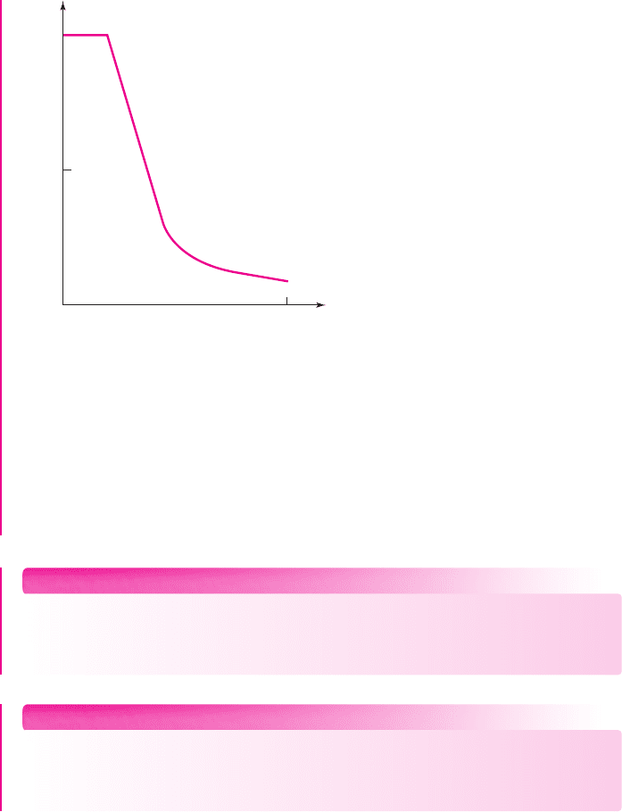
Computer Simulation: The voltage transfer characteristics of the NMOS inverter
with enhancement load shown in Figure 3.36 were obtained by a PSpice analysis.
These results are shown in Figure 3.37. As the input voltage decreases from its high
state, the output voltage increases, charging and discharging capacitances in the tran-
sistors. The current in the circuit goes to zero when the driver transistor is cutoff. This
occurs when
V
I
= V
GSD
= V
TN
= 1
V. At this point, the output voltage is
V
O
= 4V
.
Since there is no current, the capacitances cease charging and discharging so the out-
put voltage cannot get to the full
V
DD
= 5
V value. The maximum output voltage is
V
O
(
max
)
= V
DD
− V
TNL
= 5 −1 = 4
V.
nea80644_ch03_125-204.qxd 06/08/2009 08:37 PM Page 159 F506 Hard disk:Desktop Folder:MHDQ134-03:
160 Part 1 Semiconductor Devices and Basic Applications
When the input voltage is just greater than 1 V, both transistors are biased in the
saturation region as the previous analysis for
V
I
= 1.5
V showed. The output voltage
is a linear function of input voltage as we will see in Equation (3.24).
For an input voltage greater than approximately 2.25 V, the driver transistor is
biased in the nonsaturation region and the output voltage is a nonlinear function of
input voltage.
EXERCISE PROBLEM
Ex 3.9: Consider the NMOS inverter shown in Figure 3.36 with transistor para-
meters described in Example 3.9. Determine the output voltage V
O
for input volt-
ages (a)
V
I
= 4V
and (b)
V
I
= 2V
. (Ans. (a) 0.454 V, (b) 1.76 V)
COMPUTER ANALYSIS EXERCISE
PS 3.3: Consider the NMOS circuit shown in Figure 3.36. Plot the voltage trans-
fer characteristics, using a PSpice simulation. Use transistor parameters similar to
those in Example 3.9. What are the values of V
O
for
V
I
= 1.5V
and
V
I
= 5V
?
In the circuit shown in Figure 3.36, we can determine the transition point for the
driver transistor that separates the saturation and nonsaturation regions. The transi-
tion point is determined by the equation
V
DSD
(sat) = V
GSD
− V
TND
(3.22)
Again, the drain currents in the two transistors are equal. Using the saturation
drain current relationship for the driver transistor, we have
I
DD
= I
DL
(3.23(a))
or
K
nD
[V
GSD
− V
TND
]
2
= K
nL
[V
GSL
− V
TNL
]
2
(3.23(b))
4.0
2.0
0
0 5.0
V
1
(V)
V
0
(V)
Figure 3.37 Voltage transfer characteristics of NMOS inverter with enhancement load device
nea80644_ch03_125-204.qxd 06/08/2009 08:37 PM Page 160 F506 Hard disk:Desktop Folder:MHDQ134-03:

Chapter 3 The Field-Effect Transistor 161
Again, noting that
V
GSD
= V
I
and
V
GSL
= V
DSL
= V
DD
− V
O
, and taking the
square root, we have
K
nD
K
nL
(V
I
− V
TND
) = (V
DD
− V
O
− V
TNL
)
(3.24)
At the transition point, we can define the input voltage as
V
I
= V
It
and the out-
put voltage as
V
Ot
= V
DSD
(sat) = V
It
− V
TND
. Then, from Equation (3.24), the
input voltage at the transition point is
V
It
=
V
DD
− V
TNL
+ V
TND
(1 +
√
K
nD
/K
nL
)
1 +
√
K
nD
/K
nL
(3.25)
If we apply Equation (3.25) to the previous example, we can show that our initial as-
sumptions were correct.
n-Channel Depletion-Load Device
An n-channel depletion-mode MOSFET can also be used as a load device. Consider
the depletion-mode MOSFET with the gate and source connected together shown in
Figure 3.38(a). The current–voltage characteristics are shown in Figure 3.38(b). The
transistor may be biased in either the saturation or nonsaturation regions. The transi-
tion point is also shown on the plot. The threshold voltage of the n-channel depletion-
mode MOSFET is negative so that
v
DS
(sat) is positive.
A depletion-load device can be used in conjunction with another MOSFET, as
shown in Figure 3.39, to create a circuit that can be used as an amplifier or as an
inverter in a digital logic circuit. Both the load device M
L
and driver transistor M
D
may be biased in either the saturation or nonsaturation region, depending on the
value of the input voltage. We will perform the dc analysis of this circuit for a
particular dc input voltage to the gate of the driver transistor.
EXAMPLE 3.10
Objective: Determine the dc transistor currents and voltages in a circuit containing
a depletion load device.
Consider the circuit shown in Figure 3.39. Let
V
DD
= 5
V and assume transistor
parameters of
V
TND
= 1
V,
V
TNL
=−2
V,
K
nD
= 50 μ
A/V
2
, and
K
nL
= 10 μ
A/V
2
.
Determine
V
O
for
V
I
= 5
V.
V
DD
i
D
+
–
v
DS
i
D
v
DS
(sat)
v
DS
(sat) = v
GS
– V
TN
= – V
TN
v
GS
= 0
v
DS
(a)
(b)
Figure 3.38 (a) Depletion-mode NMOS device with the gate connected to the source and
(b) current–voltage characteristics
nea80644_ch03_125-204.qxd 06/08/2009 08:37 PM Page 161 F506 Hard disk:Desktop Folder:MHDQ134-03:

162 Part 1 Semiconductor Devices and Basic Applications
Solution: Assume the driver transistor M
D
is biased in the nonsaturation region and
the load transistor M
L
is biased in the saturation region. The drain currents in the two
transistors are equal. In generic form, these currents are
I
DD
= I
DL
or
K
nD
2(V
GSD
− V
TND
)V
DSD
− V
2
DSD
= K
nL
[V
GSL
− V
TNL
]
2
Since
V
GSD
= V
I
,
V
DSD
= V
O
, and
V
GSL
= 0
, then
K
nD
2(V
I
− V
TND
)V
O
− V
2
O
= K
nL
[−V
TNL
]
2
Substituting numbers, we find
(50)
2(5 − 1)V
O
− V
2
O
= (10)[−(−2)]
2
Rearranging the terms produces
5V
2
O
−40V
O
+4 = 0
Using the quadratic formula, we obtain two possible solutions:
V
O
= 7.90 V or V
O
= 0.10 V
Since the output voltage cannot be greater than the supply voltage
V
DD
= 5V
, the
valid solution is
V
O
= 0.10 V
.
The current is
I
D
= K
nL
(−V
TNL
)
2
= (10)[−(−2)]
2
= 40 μA
Comment: Since
V
DSD
= V
O
= 0.10 V < V
GSD
− V
TND
= 5 −1 = 4V
, M
D
is
biased in the nonsaturation region, as assumed. Similarly, since
V
DSL
= V
DD
− V
O
=
4.9V> V
GSL
− V
TNL
= 0 −(−2) = 2V
, M
L
is biased in the saturation region, as
originally assumed.
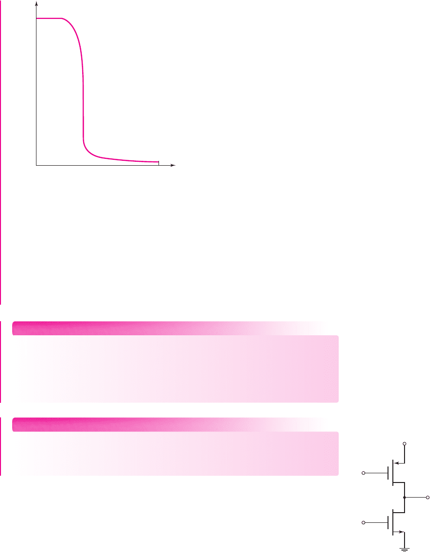
Computer Simulation: The voltage transfer characteristics of the NMOS inverter
circuit with depletion load in Figure 3.39 were obtained using a PSpice analysis.
These results are shown in Figure 3.40. For an input voltage less than 1 V, the driver
is cut off and the output voltage is
V
O
= V
DD
= 5V
.
V
DD
I
DL
I
DD
V
O
V
I
+
–
V
DSL
+
–
V
DSD
M
D
M
L
+
–
V
GSD
Load
Driver
Figure 3.39 Circuit with depletion-load device and NMOS driver
nea80644_ch03_125-204.qxd 06/08/2009 08:37 PM Page 162 F506 Hard disk:Desktop Folder:MHDQ134-03:
Chapter 3 The Field-Effect Transistor 163
When the input voltage is just greater than 1 V, the driver transistor is biased in
the saturation region and the load device in the nonsaturation region. When the input
voltage is approximately 1.9 V, both transistors are biased in the saturation region. If
the channel length modulation parameter
λ
is assumed to be zero as in this example,
there is no change in the input voltage during this transition region. As the input volt-
age becomes larger than 1.9 V, the driver is biased in the nonsaturation region and the
load in the saturation region.
EXERCISE PROBLEM
Ex 3.10: Consider the circuit shown in Figure 3.39 with transistor parameters
V
TND
= 1V
and
V
TNL
=−2V
. (a) Design the ratio
K
nD
/K
nL
that will produce
an output voltage of
V
O
= 0.25 V
at
V
I
= 5V
. (b) Find K
nD
and K
nL
if the
transistor currents are 0.2 mA when
V
I
= 5V
. (Ans. (a)
K
nD
/K
nL
= 2.06
(b)
K
nL
= 50 μA/V
2
,
K
nD
= 103 μA/V
2
)
COMPUTER ANALYSIS EXERCISE
PS 3.4: Consider the NMOS circuit shown in Figure 3.39. Plot the voltage trans-
fer characteristics using a PSpice simulation. Use transistor parameters similar to
those in Example 3.10. What are the values of V
O
for
V
I
= 1.5V
and
V
I
= 5V
?
p-Channel Enhancement-Load Device
A p-channel enhancement-mode transistor can also be used as a load device to form
a complementary MOS (CMOS) inverter. The term complementary implies that
both n-channel and p-channel transistors are used in the same circuit. The CMOS
technology is used extensively in both analog and digital electronic circuits.
Figure 3.41 shows one example of a CMOS inverter. The NMOS transistor is
used as the amplifying device, or the driver, and the PMOS device is the load, which
is referred to as an active load. This configuration is typically used in analog applications.
5.0
0
V
O
(V)
V
I
(V)
0 5.0
Figure 3.40 Voltage transfer characteristics of NMOS inverter with depletion load device
V
DD
V
O
V
I
M
N
M
P
V
G
Figure 3.41 Example of
CMOS inverter
nea80644_ch03_125-204.qxd 06/08/2009 08:37 PM Page 163 F506 Hard disk:Desktop Folder:MHDQ134-03:

164 Part 1 Semiconductor Devices and Basic Applications
In another configuration, the two gates are tied together and form the input. This con-
figuration will be discussed in detail in Chapter 16.
As with the previous two NMOS inverters, the two transistors shown in Fig-
ure 3.41 may be biased in either the saturation or nonsaturation region, depending
on the value of the input voltage. The voltage transfer characteristic is most easily
determined from a PSpice analysis.
EXAMPLE 3.11
Objective: Determine the voltage transfer characteristic of the CMOS inverter using
a PSpice analysis.
For the circuit shown in Figure 3.41, assume transistor parameters of
V
TN
= 1V
,
V
TP
=−1V
, and
K
n
= K
p
. Also assume
V
DD
= 5V
and
V
G
= 3.25 V
.
Solution: The voltage transfer characteristics are shown in Figure 3.42. In this case,
there is a region, as was the case for an NMOS inverter with depletion load, in which
both transistors are biased in the saturation region, and the input voltage is a constant
over this transition region for the assumption that the channel length modulation
parameter
λ
is zero.
Comment: In this example, the source-to-gate voltage of the PMOS device is only
V
SG
= 1.75 V
. The effective resistance looking into the drain of the PMOS device is
then relatively large. This is a desirable characteristic for an amplifier, as we will see
in the next chapter.
EXERCISE PROBLEM
Ex 3.11: Consider the circuit in Figure 3.41. Assume the same transistor parame-
ters and circuit parameters as given in Example 3.11. Determine the transition
point parameters for the transistors M
N
and M
P
. (Ans. M
P
:
V
Ot
= 4.25 V
,
V
It
=
1.75 V
; M
N
:
V
Ot
= 0.75 V
,
V
It
= 1.75 V
)
5.0
0
V
O
(V)
V
I
(V)
0 5.0
Figure 3.42 Voltage transfer characteristics of CMOS inverter in Figure 3.41
nea80644_ch03_125-204.qxd 06/08/2009 08:37 PM Page 164 F506 Hard disk:Desktop Folder:MHDQ134-03:
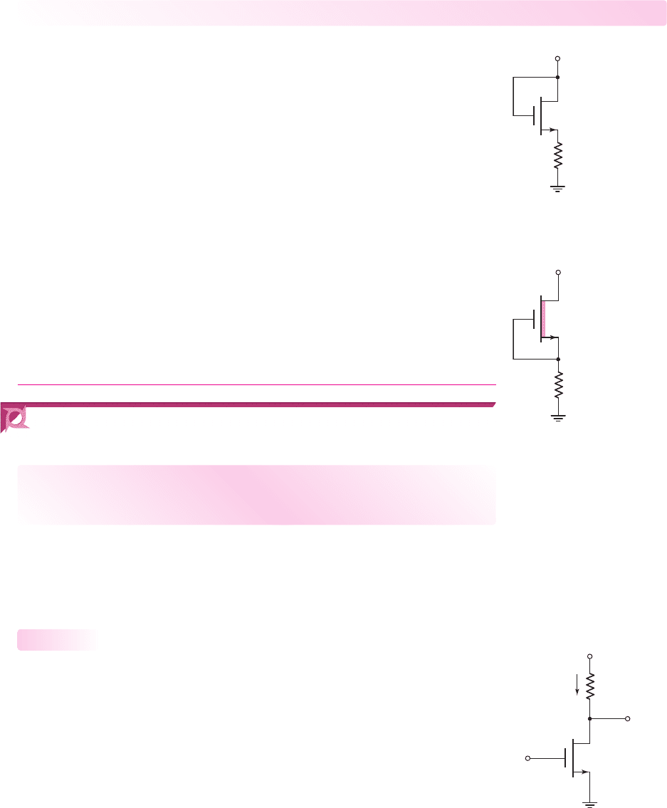
V
DD
i
D
R
D
v
O
v
I
+
–
v
DS
+
–
v
GS
Figure 3.45 NMOS inverter
circuit
Chapter 3 The Field-Effect Transistor 165
Test Your Understanding
TYU 3.7 The transistor in the circuit shown in Figure 3.25(a) has parameters
V
TN
= 0.25
V and
K
n
= 30 μ
A/V
2
. The circuit is biased at
V
DD
= 2.2
V. Let
R
1
+ R
2
= 500
k
. Redesign the circuit such that
I
DQ
= 70 μ
A and
V
DSQ
= 1.2
V.
(Ans.
R
1
= 96
k
,
R
2
= 404
k
,
R
D
= 14.3
k
)
TYU 3.8 Consider the circuit in Figure 3.43. The transistor parameters are
V
TN
= 0.4
V and
k
n
= 100 μ
A/V
2
. Design the transistor width-to-length ratio such
that
V
DS
= 1.6
V. (Ans. 2.36)
TYU 3.9 For the circuit shown in Figure 3.36, use the transistor parameters given in
Example 3.9. (a) Determine V
I
and V
O
at the transition point for the driver transistor.
(b) Calculate the transistor currents at the transition point. (Ans. (a)
V
It
= 2.236 V
,
V
Ot
= 1.236 V
; (b)
I
D
= 76.4 μA
)
TYU 3.10 Consider the circuit shown in Figure 3.44. The transistor parameters are
V
TN
=−1.2
V and
k
n
= 80 μ
A/V
2
. (a) Design the transistor width-to-length ratio
such that
V
DS
= 1.8
V. Is the transistor biased in the saturation or nonsaturation re-
gion? (b) Repeat part (a) for
V
DS
= 0.8
V. (Ans. (a) 3.26, (b) 6.10)
TYU 3.11 For the circuit shown in Figure 3.39, use the transistor parameters given in
Example 3.10. (a) Determine V
I
and V
O
at the transition point for the load transistor.
(b) Determine V
I
and V
O
at the transition point for the driver transistor. (Ans. (a)
V
It
= 1.89 V
,
V
Ot
= 3V
; (b)
V
It
= 1.89 V
,
V
Ot
= 0.89 V
)
3.3 BASIC MOSFET APPLICATIONS: SWITCH,
DIGITAL LOGIC GATE, AND AMPLIFIER
Objective: • Examine three applications of MOSFET circuits: a switch
circuit, digital logic circuit, and an amplifier circuit.
MOSFETs may be used to: switch currents, voltages, and power; perform digital logic
functions; and amplify small time-varying signals. In this section, we will examine the
switching properties of an NMOS transistor, analyze a simple NMOS transistor digi-
tal logic circuit, and discuss how the MOSFET can be used to amplify small signals.
NMOS Inverter
The MOSFET can be used as a switch in a wide variety of electronic applications.
The transistor switch provides an advantage over mechanical switches in both speed
and reliability. The transistor switch considered in this section is also called an in-
verter. Two other switch configurations, the NMOS transmission gate and the CMOS
transmission gate, are discussed in Chapter 16.
Figure 3.45 shows the n-channel enhancement-mode MOSFET inverter circuit.
If
v
I
< V
TN
, the transistor is in cutoff and
i
D
= 0
. There is no voltage drop across
R
D
, and the output voltage is
v
O
= V
DD
. Also, since
i
D
= 0
, no power is dissipated
in the transistor.
If
v
I
> V
TN
, the transistor is on and initially is biased in the saturation region,
since
v
DS
>v
GS
− V
TN
. As the input voltage increases, the drain-to-source voltage
3.3.1
Figure 3.43 Circuit for
Exercise TYU 3.8
V
DD
= 3.3 V
R
S
= 10 kΩ
V
DS
+
–
Figure 3.44 Circuit for
Exercise TYU 3.10
+
–
V
DS
V
DD
= 3.3 V
R
S
= 8 kΩ
nea80644_ch03_125-204.qxd 06/08/2009 08:37 PM Page 165 F506 Hard disk:Desktop Folder:MHDQ134-03:

166 Part 1 Semiconductor Devices and Basic Applications
decreases, and the transistor eventually becomes biased in the nonsaturation region.
When
v
I
= V
DD
, the transistor is biased in the nonsaturation region,
v
O
reaches a
minimum value, and the drain current reaches a maximum value. The current and
voltage are given by
i
D
= K
n
2(v
I
− V
TN
)v
O
−v
2
O
(3.26)
and
v
O
= v
DD
−i
D
R
D
(3.27)
where
v
O
= v
DS
and
v
I
= v
GS
.
DESIGN EXAMPLE 3.12
Objective: Design the size of a power MOSFET to meet the specification of a par-
ticular switch application.
The load in the inverter circuit in Figure 3.45 is a coil of an electromagnet that
requires a current of 0.5 A when turned on. The effective load resistance varies be-
tween 8 and 10
, depending on temperature and other variables. A 10 V power sup-
ply is available. The transistor parameters are
k
n
= 80 μA/V
2
and
V
TN
= 1V
.
Solution: One solution is to bias the transistor in the saturation region so that the
current is constant, independent of the load resistance.
The minimum
V
DS
value is 5 V. We need
V
DS
> V
DS
(sat) = V
GS
− V
TN
. If we
bias the transistor at
V
GS
= 5V
, then the transistor will always be biased in the satu-
ration region. We can then write
I
D
=
k
n
2
·
W
L
(V
GS
− V
TN
)
2
or
0.5 =
80 × 10
−6
2
W
L
· (5 − 1)
2
which yields
W/L = 781
.
The maximum power dissipation in the transistor occurs when the load resis-
tance is 8
and
V
DS
= 6
V. Then
P(max) = V
DS
(max) · I
D
= (6) · (0.5) = 3W
Comment: We see that we can switch a relatively large drain current with essen-
tially no input current to the transistor. The size of the transistor required is fairly
large, which implies a power transistor is necessary. If a transistor with a slightly
different width-to-length ratio is available, the applied
V
GS
can be changed to meet
the specification.
EXERCISE PROBLEM
Ex 3.12: For the MOS inverter circuit shown in Figure 3.45, assume the circuit
values are
V
DD
= 5
V and
R
D
= 500
. The threshold voltage of the transistor is
V
TN
= 1
V. (a) Determine the value of the conduction parameter
K
n
such that
v
O
= 0.2
V when
v
I
= 5
V. (b) What is the power dissipated in the transistor?
(Ans. (a)
K
n
= 6.15
mA/V
2
, (b)
P = 1.92
mW)
nea80644_ch03_125-204.qxd 06/08/2009 08:37 PM Page 166 F506 Hard disk:Desktop Folder:MHDQ134-03:
Chapter 3 The Field-Effect Transistor 167
Digital Logic Gate
For the transistor inverter circuit in Figure 3.45, when the input is low and approxi-
mately zero volts, the transistor is cut off, and the output is high and equal to
V
DD
.
When the input is high and equal to
V
DD
, the transistor is biased in the nonsaturation
region and the output reaches a low value. Since the input voltages will be either high
or low, we can analyze the circuit in terms of dc parameters.
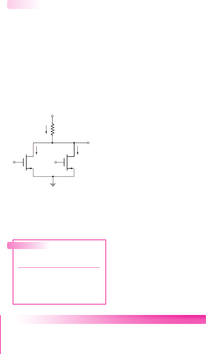
Now consider the case when a second transistor is connected in parallel, as shown in
Figure 3.46. If the two inputs are zero, both M
1
and M
2
are cut off, and
V
O
= 5V
. When
V
1
= 5V
and
V
2
= 0
, the transistor M
1
turns on and M
2
is still cut off. Transistor M
1
is
biased in the nonsaturation region, and V
O
reaches a low value. If we reverse the input
voltages such that
V
1
= 0
and
V
2
= 5V
, then M
1
is cut off and M
2
is biased in the non-
saturation region. Again, V
O
is at a low value. If both inputs are high, at
V
1
= V
2
= 5V
,
then both transistors are biased in the nonsaturation region and V
O
is low.
3.3.2
V
DD
= 5 V
V
O
V
2
V
1
R
D
M
1
M
2
I
D1
I
R
I
D2
Figure 3.46 A two-input NMOS NOR logic gate
Table 3.2 NMOS NOR logic
circuit response
V
1
(V) V
2
(V) V
O
(V)
0 0 High
50Low
05Low
55Low
Table 3.2 shows these various conditions for the circuit in Figure 3.46. In a pos-
itive logic system, these results indicate that this circuit performs the NOR logic
function, and, it is therefore called a two-input NOR logic circuit. In actual NMOS
logic circuits, the resistor R
D
is replaced by another NMOS transistor.
EXAMPLE 3.13
Objective: Determine the currents and voltages in a digital logic gate, for various
input conditions.
Consider the circuit shown in Figure 3.46 with circuit and transistor parameters
R
D
= 20 k
,
K
n
= 0.1mA/V
2
,
V
TN
= 0.8V
, and
λ = 0
.
nea80644_ch03_125-204.qxd 06/08/2009 08:37 PM Page 167 F506 Hard disk:Desktop Folder:MHDQ134-03: