Neamen D. Microelectronics: Circuit Analysis and Design
Подождите немного. Документ загружается.

178 Part 1 Semiconductor Devices and Basic Applications
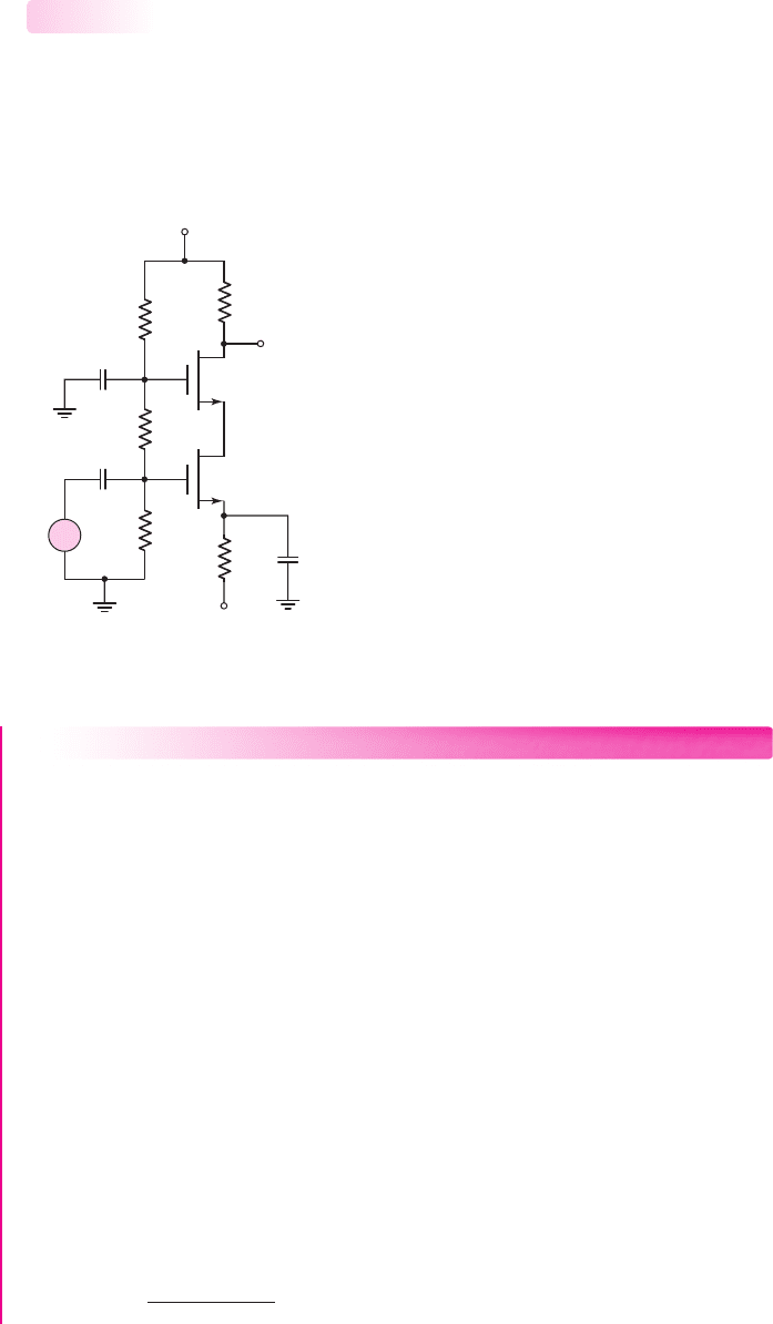
Multitransistor Circuit: Cascode Configuration
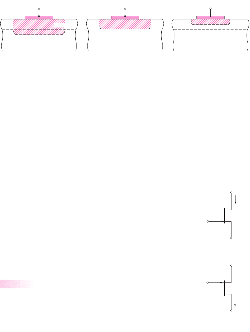
Figure 3.53 shows a cascode circuit with n-channel MOSFETs. Transistor
M
1
is con-
nected in a common-source configuration and
M
2
is connected in a common-gate
configuration. The advantage of this type of circuit is a higher frequency response,
which is discussed in a later chapter.
3.5.2
R
3
v
i
C
C
R
2
R
1
C
G
C
S
R
D
V
+
= 5 V
V
–
= –5 V
v
O
R
S
M
1
M
2
+
–
Figure 3.53 NMOS cascode circuit
DESIGN EXAMPLE 3.18
Objective: Design the biasing of the cascode circuit to meet specific requirements.
For the circuit shown in Figure 3.53, the transistor parameters are:
V
TN1
=
V
TN2
= 1.2
V,
K
n1
= K
n2
= 0.8
mA/V
2
, and
λ
1
= λ
2
= 0
. Let
R
1
+ R
2
+ R
3
=
300 k
and
R
S
= 10
k
. Design the circuit such that
I
DQ
= 0.4
mA and
V
DSQ1
= V
DSQ2
= 2.5
V.
Solution: The dc voltage at the source of
M
1
is
V
S1
= I
DQ
R
S
−5 = (0.4)(10) − 5 =−1V
Since
M
1
and
M
2
are identical transistors, and since the same current exists in the
two transistors, the gate-to-source voltage is the same for both devices. We have
I
D
= K
n
(V
GS
− V
TN
)
2
or
0.4 = 0.8(V
GS
−1.2)
2
which yields
V
GS
= 1.907 V
Then,
V
G1
=
R
3
R
1
+ R
2
+ R
3
(5) = V
GS
+ V
S1
nea80644_ch03_125-204.qxd 06/08/2009 08:37 PM Page 178 F506 Hard disk:Desktop Folder:MHDQ134-03:

Chapter 3 The Field-Effect Transistor 179
or
R
3
300
(5) = 1.907 −1 = 0.907
which yields
R
3
= 54.4k
The voltage at the source of M
2
is
V
S2
= V
DSQ1
+ V
S1
= 2.5 −1 = 1.5V
Then,
V
G2
=
R
2
+ R
3
R
1
+ R
2
+ R
3
(5) = V
GS
+ V
S2
or
R
2
+ R
3
300
(5) = 1.907 +1.5 = 3.407 V
which yields
R
2
+ R
3
= 204.4k
and
R
2
= 150 k
Therefore
R
1
= 95.6k
The voltage at the drain of M
2
is
V
D2
= V
DSQ2
+ V
S2
= 2.5 +1.5 = 4V
The drain resistor is therefore
R
D
=
5 − V
D2
I
DQ
=
5 − 4
0.4
= 2.5k
Comment: Since
V
DS
= 2.5V> V
GS
− V
TN
= 1.91 −1.2 = 0.71
V, each transis-
tor is biased in the saturation region.
EXERCISE PROBLEM
Ex 3.18: The transistor parameters for the circuit shown in Figure 3.53 are
V
TN1
= V
TN2
= 0.8V
,
K
n1
= K
n2
= 0.5
mA/V
2
, and
λ
1
= λ
2
= 0
. Let
R
1
+
R
2
+ R
3
= 500
k
and
R
S
= 16 k
. Design the circuit such that
I
DQ
=
0.25 mA
and
V
DSQ1
= V
DSQ2
= 2.5V
. (Ans.
R
3
= 50.7k
,
R
2
= 250 k
,
R
1
=
199.3k
,
R
D
= 4k
)
We will encounter many more examples of multitransistor and multistage am-
plifiers in later chapters of this text. Specifically in Chapter 11, we will consider the
differential amplifier and in Chapter 13, we will analyze circuits that form the oper-
ational amplifier.
nea80644_ch03_125-204.qxd 06/08/2009 08:37 PM Page 179 F506 Hard disk:Desktop Folder:MHDQ134-03:
180 Part 1 Semiconductor Devices and Basic Applications
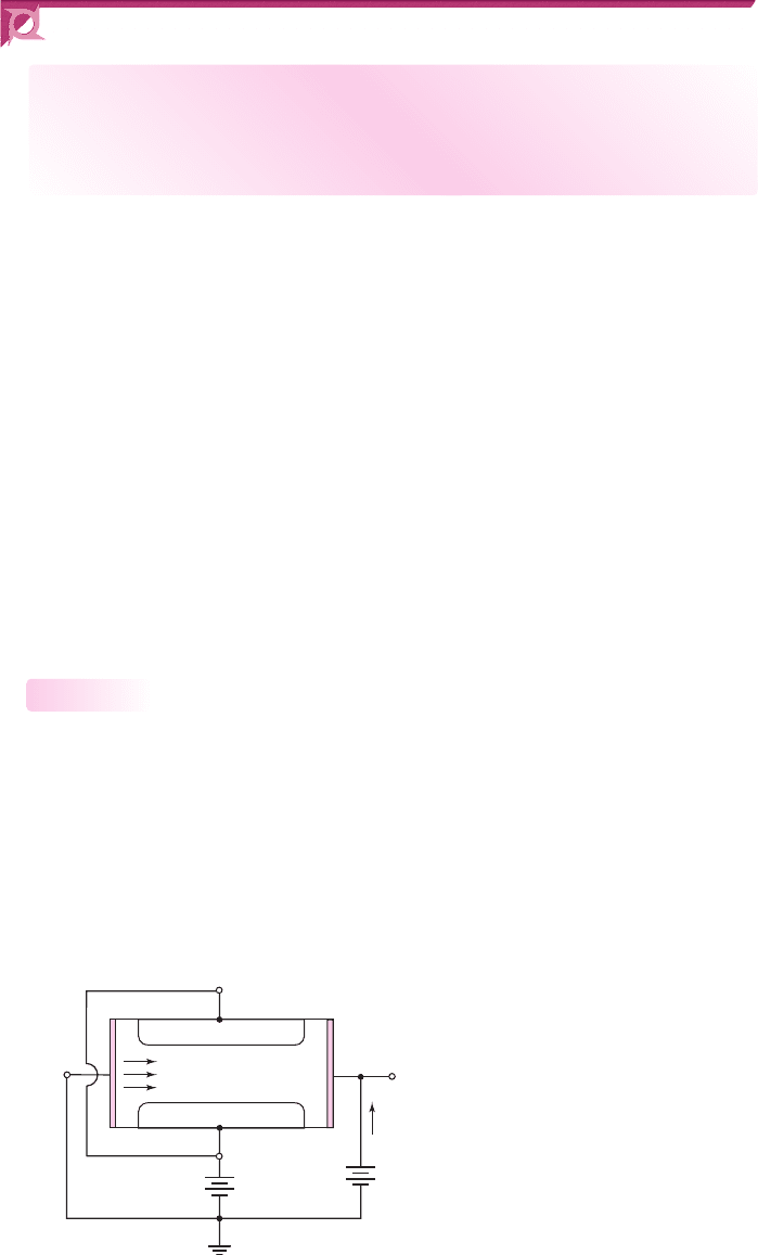
Drain
Gate
Source
Gate
+
–
v
GS
p
+
p
+
n
+
–
v
DS
e
–
e
–
e
–
i
D
Figure 3.54 Cross section of a symmetrical n-channel pn junction field-effect transistor
3.6 JUNCTION FIELD-EFFECT TRANSISTOR
Objective: • Understand the operation and characteristics of the pn
junction FET (JFET) and the Schottky barrier junction FET (MESFET),
and understand the dc analysis techniques of JFET and MESFET
circuits.
The two general categories of junction field-effect transistor (JFET) are the pn
junction FET, or pn JFET, and the metal-semiconductor field-effect transistor
(MESFET), which is fabricated with a Schottky barrier junction.
The current in a JFET is through a semiconductor region known as the channel,
with ohmic contacts at each end. The basic transistor action is the modulation of the
channel conductance by an electric field perpendicular to the channel. Since the
modulating electric field is induced in the space-charge region of a reverse-biased
pn junction or Schottky barrier junction, the field is a function of the gate voltage. Mod-
ulation of the channel conductance by the gate voltage modulates the channel current.
JFETs were developed before MOSFETs, but the applications and uses of the
MOSFET have far surpassed those of the JFET. One reason is that the voltages ap-
plied to the gate and drain of a MOSFET are the same polarity (both positive or both
negative), whereas the voltages applied to the gate and drain of most JFETs must
have opposite polarities. Since the JFET is used only in specialized applications, our
discussion will be brief.
pn JFET and MESFET Operation
pn JFET
A simplified cross section of a symmetrical pn JFET is shown in Figure 3.54. In the
n-region channel between the two p-regions, majority carrier electrons flow from
the source to the drain terminal; thus, the JFET is called a majority-carrier device.
The two gate terminals shown in Figure 3.54 are connected to form a single gate.
In a p-channel JFET, the p- and n-regions are reversed from those of the n-
channel device, and holes flow in the channel from the source to the drain. The
current direction and voltage polarities in the p-channel JFET are reversed from
3.6.1
nea80644_ch03_125-204.qxd 06/08/2009 08:37 PM Page 180 F506 Hard disk:Desktop Folder:MHDQ134-03:
Chapter 3 The Field-Effect Transistor 181
those in the n-channel device. Also, the p-channel JFET is generally a lower-
frequency device than the n-channel JFET, because hole mobility is lower than elec-
tron mobility.
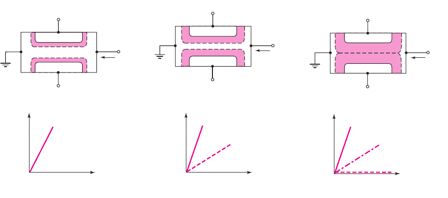
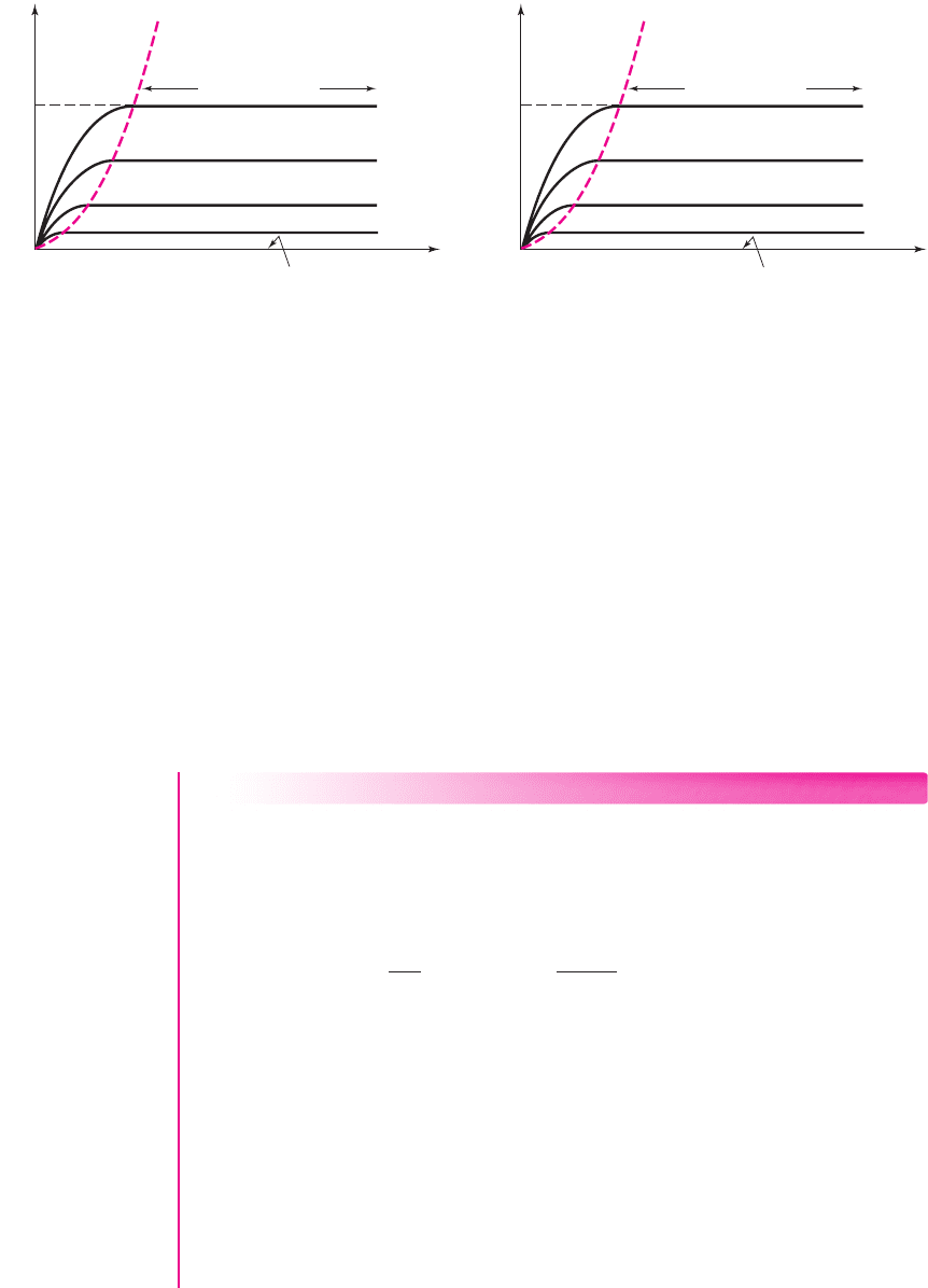
Figure 3.55(a) shows an n-channel JFET with zero volts applied to the gate. If
the source is at ground potential, and if a small positive drain voltage is applied, a
drain current
i
D
is produced between the source and drain terminals. Since the
n-channel acts essentially as a resistance, the
i
D
versus
v
DS
characteristic for small
v
DS
values is approximately linear, as shown in the figure.
If a voltage is applied to the gate of a pn JFET, the channel conductance changes.
If a negative gate voltage is applied to the n-channel pn JFET in Figure 3.55, the gate-
to-channel pn junction becomes reverse biased. The space-charge region widens, the
channel region narrows, the resistance of the n-channel increases, and the slope of the
i
D
versus
v
DS
curve, for small
v
DS
, decreases. These effects are shown in Figure 3.55(b).
If a larger negative gate voltage is applied, the condition shown in Figure 3.55(c) can
be achieved. The reverse-biased gate-to-channel space-charge region completely fills
the channel region. This condition is known as pinchoff. Since the depletion region
isolates the source and drain terminals, the drain current at pinchoff is essentially
zero. The
i
D
versus
v
DS
curves are shown in Figure 3.55(c). The current in the chan-
nel is controlled by the gate voltage. The control of the current in one part of the de-
vice by a voltage in another part of the device is the basic transistor action. The pn
JFET is a “normally on,” or depletion mode, device; that is, a voltage must be applied
to the gate terminal to turn the device off.
Consider the situation in which the gate voltage is zero,
v
GS
= 0
, and the drain
voltage changes, as shown in Figure 3.56(a). As the drain voltage increases (posi-
tive), the gate-to-channel pn junction becomes reverse biased near the drain terminal,
and the space-charge region widens, extending farther into the channel. The channel
acts essentially as a resistor, and the effective channel resistance increases as the
space-charge region widens; therefore, the slope of the
i
D
versus
v
DS
characteristic
i
D
i
D
p
+
p
+
v
DS
+v
DS
v
GS
= 0
v
GS
= 0
v
GS
= 0
i
D
p
+
p
+
i
D
v
DS
+v
DS
v
GS
= −V
1
v
GS
= −V
1
v
GS
= 0
v
GS
= −V
1
(a) (b)
v
DS
i
D
i
D
+v
D
S
v
GS
= 0
v
GS
= −V
2
v
GS
= −V
2
v
GS
= −V
2
v
GS
= −V
1
p
+
p
+
(c)
Figure 3.55 Gate-to-channel space-charge regions and current–voltage characteristics for
small drain-to-source voltages and for: (a) zero gate voltage, (b) small reverse-biased
gate voltage, and (c) a gate voltage that achieves pinchoff
nea80644_ch03_125-204.qxd 06/08/2009 08:37 PM Page 181 F506 Hard disk:Desktop Folder:MHDQ134-03:
182 Part 1 Semiconductor Devices and Basic Applications
decreases, as shown in Figure 3.56(b). The effective channel resistance now varies
along the channel length, and, since the channel current must be constant, the voltage
drop through the channel becomes dependent on position.
If the drain voltage increases further, the condition shown in Figure 3.56(c) can
result. The channel is pinched off at the drain terminal. Any further increase in drain
voltage will not increase the drain current. The
i
D
–v
DS
characteristic for this condi-
tion is also shown in the figure. The drain voltage at pinchoff is
v
DS
(sat)
. Therefore,
for
v
DS
>v
DS
(sat)
, the transistor is biased in the saturation region, and the drain cur-
rent for this ideal case is independent of
v
DS
.
MESFET
In the MESFET, the gate junction is a Schottky barrier junction, instead of a pn junc-
tion. Although MESFETs can be fabricated in silicon, they are usually associated
with gallium arsenide or other compound-semiconductor materials.
A simplified cross section of a GaAs MESFET is shown in Figure 3.57. A thin,
epitaxial layer of GaAs is used for the active region; the substrate is a very high re-
sistivity GaAs material, referred to as a semi-insulating substrate. The advantages of
i
D
p
+
p
+
i
D
v
DS
(+v
DS
)
v
GS
= 0
v
GS
= 0
i
D
i
D
v
DS
(++v
DS
)
v
GS
= 0
p
+
p
+
v
GS
= 0
Changing channel
resistance
i
D
i
D
v
DS
(+++v
DS
)
v
GS
= 0
p
+
p
+
v
GS
= 0
v
DS
(sat)
Saturation
region
(a) (b) (c)
Figure 3.56 Gate-to-channel space-charge regions and current–voltage characteristics for
zero gate voltage and for: (a) a small drain voltage, (b) a larger drain voltage, and (c) a drain
voltage that achieves pinchoff at the drain terminal
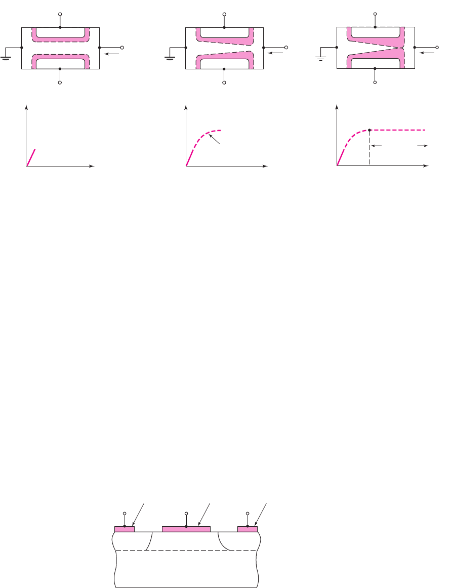
Substrate
(Semi-insulating s
≈ 0)
Rectifying
contact
Ohmic
contac
t
Ohmic
contact
Source Gate Drain
n
+
n
+
n
Figure 3.57 Cross section of an n-channel MESFET with a semi-insulating substrate
nea80644_ch03_125-204.qxd 06/08/2009 08:37 PM Page 182 F506 Hard disk:Desktop Folder:MHDQ134-03:
Chapter 3 The Field-Effect Transistor 183
these devices include: higher electron mobility in GaAs, hence smaller transit time
and faster response; and decreased parasitic capacitance and a simplified fabrication
process, resulting from the semi-insulating GaAs substrate.
In the MESFET in Figure 3.57, a reverse-bias gate-to-source voltage induces a
space-charge region under the metal gate, which modulates the channel conductance,
as in the case of the pn JFET. If a negative applied gate voltage is sufficiently large,
the space-charge region will eventually reach the substrate. Again, pinchoff will
occur. Also, the device shown in the figure is a depletion mode device, since a gate
voltage must be applied to pinch off the channel, that is, to turn the device off.
In another type of MESFET, the channel is pinched off even at
v
GS
= 0
,as
shown in Figure 3.58(a). For this MESFET, the channel thickness is smaller than the
zero-biased space-charge width. To open a channel, the depletion region must be re-
duced; that is, a forward-biased voltage must be applied to the gate–semiconductor
junction. When a slightly forward-bias voltage is applied, the depletion region ex-
tends just to the width of the channel as shown in Figure 3.58(b). The threshold
voltage is the gate-to-source voltage required to create the pinchoff condition.
The threshold voltage for this n-channel MESFET is positive, in contrast to the
negative threshold voltage of the n-channel depletion-mode device. If a larger
forward-bias voltage is applied, the channel region opens, as shown in Figure
3.58(c). The applied forward-bias gate voltage is limited to a few tenths of a volt be-
fore a significant gate current occurs.
This device is an n-channel enhancement-mode MESFET. Enhancement-
mode p-channel MESFETs and enhancement-mode pn JFETs have also been fabri-
cated. The advantage of enhancement-mode MESFETs is that circuits can be
designed in which the voltage polarities on the gate and drain are the same. However,
the output voltage swing of these devices is quite small.
Current–Voltage Characteristics
The circuit symbols for the n-channel and p-channel JFETs are shown in Figure 3.59,
along with the gate-to-source voltages and current directions. The ideal current–
voltage characteristics, when the transistor is biased in the saturation region, are
described by
i
D
= I
DSS
1 −
v
GS
V
P
2
(3.32)
where
I
DSS
is the saturation current when
v
GS
= 0
, and
V
P
is the pinchoff voltage.
3.6.2
v
GS
> V
TN
(c)
v
GS
= V
TN
(b)
Semi-insulating substrate
v
GS
= 0
(a)
n-channel
Figure 3.58 Channel space-charge region of an enhancement-mode MESFET for:
(a)
v
GS
= 0
, (b)
v
GS
= V
TN
, and (c)
v
GS
> V
TN
v
GS
v
DS
G
S
D
+
+
–
–
i
D
v
GS
v
SD
G
S
D
+
+
–
–
i
D
(a)
(b)
Figure 3.59 Circuit symbols
for: (a) n-channel JFET and
(b) p-channel JFET
nea80644_ch03_125-204.qxd 06/08/2009 08:37 PM Page 183 F506 Hard disk:Desktop Folder:MHDQ134-03:
184 Part 1 Semiconductor Devices and Basic Applications
The current–voltage characteristics for n-channel and p-channel JFETs are
shown in Figures 3.60(a) and 3.60(b), respectively. Note that the pinchoff voltage
V
P
for the n-channel JFET is negative and the gate-to-source voltage
v
GS
is usually neg-
ative; therefore, the ratio
v
GS
/V
P
is positive. Similarly, the pinchoff voltage
V
P
for
the p-channel JFET is positive and the gate-to-source voltage
v
GS
must be positive,
and therefore the ratio
v
GS
/V
P
is positive.
For the n-channel device, the saturation region occurs when
v
DS
≥ v
DS
(sat)
where
v
DS
(sat) = v
GS
− V
P
(3.33)
For the p-channel device, the saturation region occurs when
v
SD
≥ v
SD
(sat)
where
v
SD
(sat) = V
P
−v
GS
(3.34)
EXAMPLE 3.19
Objective: Calculate
i
D
and
v
DS
(sat)
in an n-channel pn JFET.
Assume the saturation current is
I
DSS
= 2mA
and the pinchoff voltage is
V
P
=−3.5
V. Calculate
i
D
and
v
DS
(sat)
for
v
GS
= 0
,
V
P
/4
, and
V
P
/2
.
Solution: From Equation (3.32), we have
i
D
= I
DSS
1 −
v
GS
V
P
2
= (2)
1 −
v
GS
(−3.5)
2
Therefore, for
v
GS
= 0
,
V
P
/4
,and
V
P
/2
, we obtain
i
D
= 2, 1.13, and 0.5mA
From Equation (3.33), we have
v
DS
(sat) = v
GS
− V
P
= v
GS
−(−3.5)
Therefore, for
v
GS
= 0
,
V
P
/4
,and
V
P
/2
, we obtain
v
DS
(sat) = 3.5, 2.63, and 1.75 V
Comment: The current capability of a JFET can be increased by increasing the
value of
I
DSS
, which is a function of the transistor width.
I
DSS
i
D
–1
– 3
– 2
v
GS
= 0
v
GS
≤ V
P
v
DS
Saturation region
I
DSS
i
D
+1
+3
+2
v
GS
= 0
v
GS
≥ V
P
v
SD
Saturation region
(a) (b)
Figure 3.60 Current–voltage characteristics for: (a) n-channel JFET and (b) p-channel JFET
nea80644_ch03_125-204.qxd 06/08/2009 08:37 PM Page 184 F506 Hard disk:Desktop Folder:MHDQ134-03:

Chapter 3 The Field-Effect Transistor 185
EXERCISE PROBLEM
Ex 3.19: The parameters of an n-channel JFET are
I
DSS
= 12 mA
,
V
P
=−4.5V
, and
λ = 0
. Determine
V
DS
(sat)
for
V
GS
=−1.2V
, and calculate
I
D
for
V
DS
> V
DS
(sat)
. (Ans.
V
DS
(sat) = 3.3V
,
I
D
= 6.45 mA
)
As in the case of the MOSFET, the
i
D
versus
v
DS
characteristic for the JFET
may have a nonzero slope beyond the saturation point. This nonzero slope can be de-
scribed through the following equation:
i
D
= I
DSS
1 −
v
GS
V
P
2
(1 + λv
DS
)
(3.35)
The output resistance
r
o
is defined as
r
o
=
∂i
D
∂v
DS
−1
v
GS
=const.
(3.36)
Using Equation (3.35), we find that
r
o
=
λI
DSS
1 −
V
GSQ
V
P
2
−1
(3.37(a))
or
r
o
∼
=
[λI
DQ
]
−1
=
1
λI
DQ
(3.37(b))
The output resistance will be considered again when we discuss the small-signal
equivalent circuit of the JFET in the next chapter.
Enhancement-mode GaAs MESFETs can be fabricated with current–voltage
characteristics much like those of the enhancement-mode MOSFET. Therefore, for
the ideal enhancement-mode MESFET biased in the saturation region, we can write
i
D
= K
n
(v
GS
− V
TN
)
2
(3.38(a))
For the ideal enhancement-mode MESFET biased in the nonsaturation region,
i
D
= K
n
2(v
GS
− V
TN
)v
DS
−v
2
DS
(3.38(b))
where
K
n
is the conduction parameter and
V
TN
is the threshold voltage, which in this
case is equivalent to the pinchoff voltage. For an n-channel enhancement-mode
MESFET, the threshold voltage is positive.
Common JFET Configurations: dc Analysis
There are several common JFET circuit configurations. We will look at a few of
these, using examples, and will illustrate the dc analysis and design of such circuits.
DESIGN EXAMPLE 3.20
Objective: Design a JFET circuit with a voltage divider biasing circuit.
Consider the circuit shown in Figure 3.61(a) with transistor parameters
I
DSS
= 12 mA
,
V
P
=−3.5V
, and
λ = 0
. Let
R
1
+ R
2
= 100 k
. Design the cir-
cuit such that the dc drain current is
I
D
= 5mA
and the dc drain-to-source voltage is
V
DS
= 5V
.
3.6.3
nea80644_ch03_125-204.qxd 06/08/2009 08:37 PM Page 185 F506 Hard disk:Desktop Folder:MHDQ134-03:
186 Part 1 Semiconductor Devices and Basic Applications
Solution: Assume the transistor is biased in the saturation region. The dc drain cur-
rent is then given by
I
D
= I
DSS
1 −
V
GS
V
P
2
Therefore,
5 = 12
1 −
V
GS
(−3.5)
2
which yields
V
GS
=−1.24 V
From Figure 3.61(b), the voltage at the source terminal is
V
S
= I
D
R
S
−5 = (5)(0.5) − 5 =−2.5V
which means that the gate voltage is
V
G
= V
GS
+ V
S
=−1.24 − 2.5 =−3.74 V
We can also write the gate voltage as
V
G
=
R
2
R
1
+ R
2
(10) − 5
or
−3.74 =
R
2
100
(10) − 5.
+
–
V
DS
R
S
= 0.5 kΩ
R
S
= 0.5 kΩ
V
S
V
G
R
D
I
D
R
1
R
2
R
2
R
1
+5 V
–5 V –5 V
I
D
=
5 mA
I
D
=
5 mA
+5 V
2.5
5
R
D
= = 0.5 kΩ
V
D
= V
S
+ V
DS
= 2.5 V
V
G
= V
S
+ V
GS
= –2.5 – 1.24
= –3.74 V
V
S
= (5)(.05) – 5
= –2.5 V
V
DS
= 5 V
0
V
GS
+
+
–
–
(a) (b)
Figure 3.61 (a) An n-channel JFET circuit with voltage divider biasing and
(b) the n-channel JFET circuit for Example 3.20
nea80644_ch03_125-204.qxd 06/08/2009 08:37 PM Page 186 F506 Hard disk:Desktop Folder:MHDQ134-03:
Chapter 3 The Field-Effect Transistor 187
Therefore,
R
2
= 12.6k
and
R
1
= 87.4k
The drain-to-source voltage is
V
DS
= 5 − I
D
R
D
− I
D
R
S
−(−5)
Therefore,
R
D
=
10 − V
DS
− I
D
R
S
I
D
=
10 − 5 −(5)(0.5)
5
= 0.5k
We also see that
V
DS
= 5V> V
GS
− V
P
=−1.24 − (−3.5) = 2.26 V
which shows that the JFET is indeed biased in the saturation region, as initially
assumed.
Comment: The dc analysis of the JFET circuit is essentially the same as that of the
MOSFET circuit, since the gate current is assumed to be zero.
EXERCISE PROBLEM
Ex 3.20: The transistor in the circuit in Figure 3.62 has parameters
I
DSS
= 6mA
,
V
P
=−4V
, and
λ = 0
. Design the circuit such that
I
DQ
= 2.5mA
and
V
DS
= 6V
, and the total power dissipated in
R
1
and
R
2
is 2 mW. (Ans.
R
D
= 1.35 k
,
R
1
= 158 k
,
R
2
= 42 k
)
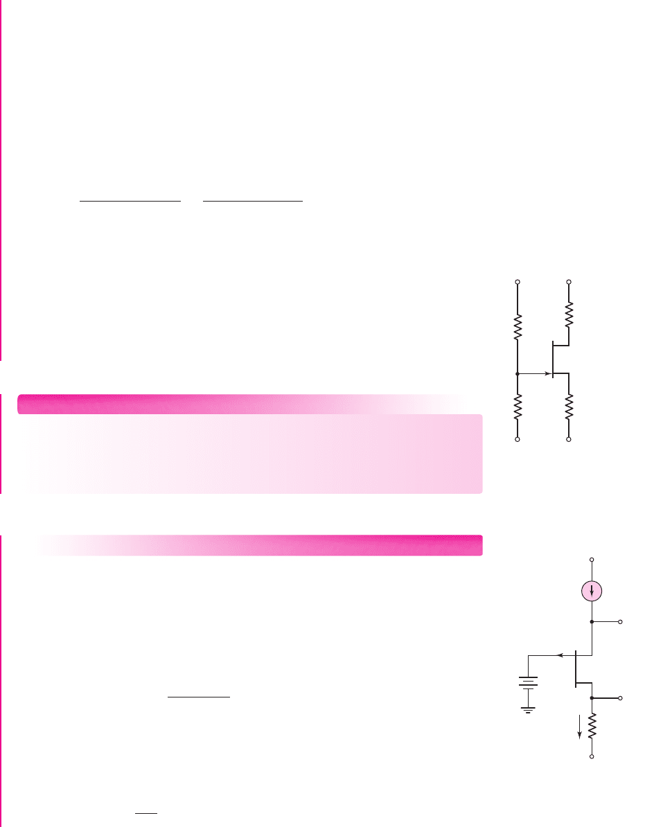
EXAMPLE 3.21
Objective: Calculate the quiescent current and voltage values in a p-channel JFET
circuit.
The parameters of the transistor in the circuit shown in Figure 3.63 are:
I
DSS
= 2.5mA
,
V
P
=+2.5V
, and
λ = 0
. The transistor is biased with a constant-
current source.
Solution: From Figure 3.63, we can write the dc drain current as
I
D
= I
Q
= 0.8mA=
V
D
−(−9)
R
D
which yields
V
D
= (0.8)(4) − 9 =−5.8V
Now, assume the transistor is biased in the saturation region. We then have
I
D
= I
DSS
1 −
V
GS
V
P
2
Figure 3.62 Circuit for
Exercise Ex 3.20
R
S
= 0.25 kΩ
R
2
R
1
–10 V –5 V
+10 V +5 V
R
D
R
D
= 4 kΩ
I
Q
= 0.8 mA
–9 V
V
GS
+
–
+9 V
V
S
V
D
V
SD
+
–
+
1 V
–
I
D
Figure 3.63 A p-channel
JFET circuit biased with a
constant-current source
nea80644_ch03_125-204.qxd 06/08/2009 08:37 PM Page 187 F506 Hard disk:Desktop Folder:MHDQ134-03: