Neamen D. Microelectronics: Circuit Analysis and Design
Подождите немного. Документ загружается.


168 Part 1 Semiconductor Devices and Basic Applications
Solution: For
V
1
= V
2
= 0
, both M
1
and M
2
are cut off and
V
O
= V
DD
= 5V
. For
V
1
= 5V
and
V
2
= 0
, the transistor M
1
is biased in the nonsaturation region, and we
can write
I
R
= I
D1
=
5 − V
O
R
D
= K
n
2(V
1
− V
TN
)V
O
− V
2
O
Solving for the output voltage V
O
, we obtain
V
O
= 0.29 V
.
The currents are
I
R
= I
D1
=
5 − 0.29
20
= 0.236 mA
For
V
1
= 0
and
V
2
= 5V
, we have
V
O
= 0.29 V
and
I
R
= I
D2
= 0.236 mA
.
When both inputs go high to
V
1
= V
2
= 5V
, we have
I
R
= I
D1
+ I
D2
,or
5 − V
O
R
D
= K
n
2(V
1
− V
TN
)V
O
− V
2
O
+ K
n
2(V
2
− V
TN
)V
O
− V
2
O
which can be solved for V
O
to yield
V
O
= 0.147 V
.
The currents are
I
R
=
5 − 0.147
20
= 0.243 mA
and
I
D1
= I
D2
=
I
R
2
= 0.121 mA
Comment: When either transistor is biased on, it is biased in the nonsaturation
region, since
V
DS
< V
DS
(sat)
, and the output voltage reaches a low state.
EXERCISE PROBLEM
Ex 3.13: For the circuit in Figure 3.46, assume the circuit and transistor parame-
ters are:
R
D
= 30 k
,
V
TN
= 1V
, and
K
n
= 50 μA/V
2
. Determine V
O
, I
R
, I
D1
,
and I
D2
for: (a)
V
1
= 5V
,
V
2
= 0
; and (b)
V
1
= V
2
= 5V
. (Ans. (a)
V
O
= 0.40 V
,
I
R
= I
D1
= 0.153 mA
,
I
D2
= 0
(b)
V
O
= 0.205 V
,
I
R
= 0.16 mA
,
I
D1
= I
D2
=
0.080 mA
)
This example and discussion illustrates that MOS transistors can be configured
in a circuit to perform logic functions. A more detailed analysis and design of
MOSFET logic gates and circuits is presented in Chapter 16. As we will see in that
chapter, most MOS logic gate circuits are fabricated by using CMOS, which means
designing circuits with both n-channel and p-channel transistors and no resistors.
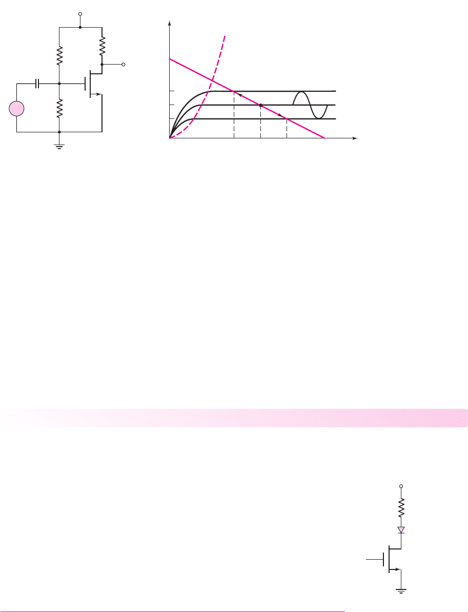
MOSFET Small-Signal Amplifier
The MOSFET, in conjunction with other circuit elements, can amplify small time-
varying signals. Figure 3.47(a) shows the MOSFET small-signal amplifier, which is
a common-source circuit in which a time-varying signal is coupled to the gate
through a coupling capacitor. Figure 3.47(b) shows the transistor characteristics and
the load line. The load line is determined for
v
i
= 0
.
3.3.3
nea80644_ch03_125-204.qxd 06/08/2009 08:37 PM Page 168 F506 Hard disk:Desktop Folder:MHDQ134-03:
Chapter 3 The Field-Effect Transistor 169
We can establish a particular Q-point on the load line by designing the ratio of
the bias resistors
R
1
and
R
2
. If we assume that
v
i
= V
i
sin ωt
, the gate-to-source volt-
age will have a sinusoidal signal superimposed on the dc quiescent value. As
the gate-to-source voltage changes over time, the Q-point will move up and down the
line, as indicated in the figure.
Moving up and down the load line translates into a sinusoidal variation in the
drain current and in the drain-to-source voltage. The variation in output voltage can
be larger than the input signal voltage, which means the input signal is amplified. The
actual signal gain depends on both the transistor parameters and the circuit element
values.
In the next chapter, we will develop an equivalent circuit for the transistor used
to determine the time-varying small-signal gain and other characteristics of the
circuit.
Test Your Understanding
TYU 3.12 The circuit shown in Figure 3.45 is biased at
V
DD
= 10
V, and the transistor
parameters are
V
TN
= 0.7
V and
K
n
= 4
mA/V
2
. Design the value of
R
D
such that the
output voltage will be
v
O
= 0.20
V when
v
I
= 10
V. (Ans. 0.666 k
)
TYU 3.13 The transistor in the circuit shown in Figure 3.48 has parameters
K
n
=
4 mA/V
2
and
V
TN
= 0.8
V, and is used to switch the LED on and off. The LED
cutin voltage is
V
γ
= 1.5
V. The LED is turned on by applying an input voltage
of
v
I
= 5
V. (a) Determine the value of R such that the diode current is 12 mA.
(b) From the results of part (a), what is the value of
v
DS
? (Ans. (a)
R = 261
,
(b)
v
DS
= 0.374
V)
TYU 3.14 In the circuit in Figure 3.46, let
R
D
= 25
k
and
V
TN
= 1
V. (a) Deter-
mine the value of the conduction parameter
K
n
required such that
V
O
= 0.10
V when
V
1
= 0
and
V
2
= 5
V. (b) Using the results of part (a), find the value of
V
O
when
V
1
= V
2
= 5
V. (Ans. (a)
K
n
= 0.248
mA/V
2
, (b)
V
O
= 0.0502
V)
R
1
V
DD
R
2
R
D
v
O
v
i
+
+
–
–
v
DS
v
GS
C
C
i
D
I
DQ
V
DS
V
DSQ
V
DS
V
GS
V
GSQ
V
GS
V
DD
v
DS
(sat)
v
D
S
I
DQ
+
+
+
I
DQ
–
–
–
(a) (b)
+
–
Figure 3.47 (a) An NMOS common-source circuit with a time-varying signal coupled to the
gate and (b) transistor characteristics, load line, and superimposed sinusoidal signals
5
V
R
v
I
LED
Figure 3.48
nea80644_ch03_125-204.qxd 06/08/2009 08:37 PM Page 169 F506 Hard disk:Desktop Folder:MHDQ134-03:
170 Part 1 Semiconductor Devices and Basic Applications
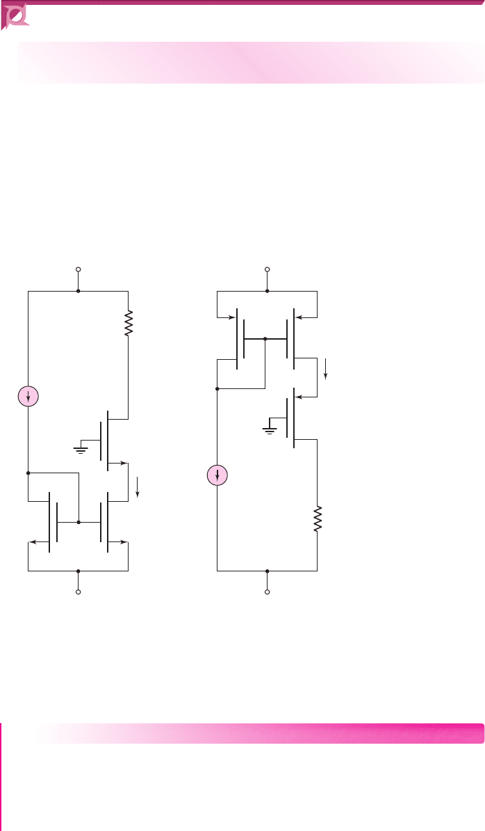
3.4 CONSTANT-CURRENT BIASING
Objective: • Investigate current biasing of MOSFET devices.
As was shown in Figure 3.32, a MOSFET can be biased with a constant-current
source
I
Q
. The gate-to-source voltage of the transistor in this circuit then adjusts
itself to correspond to the current
I
Q
.
We can implement the current source by using MOSFET devices. The circuits
shown in Figures 3.49(a) and 3.49(b) are a first step toward this design. The transis-
tors
M
2
and
M
3
in Figure 3.49(a) form a current mirror and are used to bias the
NMOS transistor
M
1
. Similarly, the transistors
M
B
and
M
C
in Figure 3.49(b) form a
current mirror and are used to bias the PMOS transistor
M
A
.
I
Q1
I
Q2
V
GS3
V
GS2
V
GS1
V
DS1
M
A
M
B
M
C
V
SDA
V
SGB
V
SGC
V
–
V
–
V
+
V
+
M
2
I
REF1
I
REF2
M
1
M
3
R
D
= 8 kΩ
R
D
= 8 kΩ
+
+
+
+
–
–
––
+
++
–
V
SGA
+
–
–
–
(a) (b)
Figure 3.49 (a) NMOS current mirror and (b) PMOS current mirror
The operation and characteristics of these circuits are demonstrated in the
following two examples.
EXAMPLE 3.14
Objective: Analyze the circuit shown in Figure 3.49(a). Determine the bias current
I
Q1
,
the gate-to-source voltages of the transistors, and the drain-to-source voltage of
M
1
.
Assume circuit parameters of
I
REF1
= 200 μ
A,
V
+
= 2.5
V, and
V
−
=−2.5
V.
Assume transistor parameters of
V
TN
= 0.4
V (all transistors),
λ = 0
(all transis-
tors),
K
n1
= 0.25
mA/V
2
, and
K
n2
= K
n3
= 0.15
mA/V
2
.
nea80644_ch03_125-204.qxd 06/08/2009 08:37 PM Page 170 F506 Hard disk:Desktop Folder:MHDQ134-03:

Chapter 3 The Field-Effect Transistor 171
Solution:
The drain current in
M
3
is
I
D3
= I
REF1
= 200 μ
A and is given by the re-
lation
I
D3
= K
n3
(V
GS3
− V
TN
)
2
(the transistor is biased in the saturation region).
Solving for the gate-to-source voltage, we find
V
GS3
=
I
D3
K
n3
+ V
TN
=
0.2
0.15
+0.4
or
V
GS3
= 1.555 V
We note that
V
GS3
= V
GS2
= 1.555
V. We can write
I
D2
= I
Q1
= K
n2
(V
GS2
− V
TN
)
2
= 0.15(1.555 −0.4)
2
or
I
Q1
= 200 μA
The gate-to-source voltage
V
GS1
(assuming
M
1
is biased in the saturation region) can
be written as
V
GS1
=
I
Q1
K
n1
+ V
TN
=
0.2
0.25
+0.4
or
V
GS1
= 1.29 V
The drain-to-source voltage is found from
V
DS1
= V
+
− I
Q1
R
D
−(−V
GS1
)
= 2.5 −(0.2)(8) −(−1.29)
or
V
DS1
= 2.19 V
We may note that
M
1
is indeed biased in the saturation region.
Comment: Since the current mirror transistors
M
2
and
M
3
are matched (identical
parameters) and since the gate-to-source voltages are the same in the two transistors,
the bias current,
I
Q1
, is equal to (i.e., mirrors) the reference current,
I
REF1
.
EXERCISE PROBLEM
Ex 3.14: For the circuit shown in Figure 3.49(a), assume circuit parameters of
I
REF1
= 120 μ
A,
V
+
= 3
V, and
V
−
=−3
V; and assume transistor parameters
of
V
TN
= 0.4
V,
λ = 0
,
K
n1
= 50 μ
A/V
2
,
K
n2
= 30 μ
A/V
2
, and
K
n3
= 60
μ
A/V
2
. Determine
I
Q1
and all gate-to source voltages. (Ans.
I
Q1
= 60 μ
A,
V
GS1
= 1.495
V,
V
GS2
= V
GS3
= 1.814
V)
We will now consider a current mirror in which the bias current and reference current
are not equal.
EXAMPLE 3.15
Objective: Design the circuit shown in Figure 3.49(b) to provide a bias current of
I
Q2
= 150 μ
A.
nea80644_ch03_125-204.qxd 06/08/2009 08:37 PM Page 171 F506 Hard disk:Desktop Folder:MHDQ134-03:

172 Part 1 Semiconductor Devices and Basic Applications
Assume circuit parameters of I
REF2
= 250
μ
A,
V
+
= 3
V, and
V
−
=−3
V. As-
sume transistor parameters of
V
TP
=−0.6
V (all transistors),
λ = 0
(all transistors),
k
p
= 40 μ
A/V
2
(all transistors),
W/L
C
= 15
, and
W/L
A
= 25
.
Solution: Since the bias current
I
Q2
and reference current I
REF2
are not equal, the
W/L
ratios of the current mirror transistors, M
C
and M
B
, will not be the same.
For M
C
, since the transistor is biased in the saturation region, we have
I
DC
= I
REF2
=
k
p
2
·
W
L
C
(V
SGC
+ V
TP
)
2
or
250 =
40
2
(15)[V
SGC
+(−0.6)]
2
= 300(V
SGC
−0.6)
2
Then
V
SGC
=
250
300
+0.6
or
V
SGC
= 1.513 V
Since
V
SGC
= V
SGB
= 1.513
V, we obtain
I
B
= I
Q2
=
k
p
2
·
W
L
B
(V
SGB
+ V
TP
)
2
or
150 =
40
2
·
W
L
B
[1.513 + (−0.6)]
2
We find
W
L
B
= 9
For M
A
, we have
I
DA
= I
Q2
=
k
p
2
·
W
L
A
(V
SGA
+ V
TP
)
2
or
150 =
40
2
(25)(V
SGA
+(−0.6))
2
= 500(V
SGA
−0.6)
2
Now
V
SGA
=
150
500
+0.6
or
V
SGA
= 1.148 V
The source-to-drain voltage of M
A
is found from
V
SDA
= V
SGA
− I
Q2
R
D
− V
−
= 1.148 −(0.15)(8) − (−3)
nea80644_ch03_125-204.qxd 06/08/2009 08:37 PM Page 172 F506 Hard disk:Desktop Folder:MHDQ134-03:
Chapter 3 The Field-Effect Transistor 173
or
V
SDA
= 2.95 V
We may note that the transistor M
A
is biased in the saturation region.
Comment: By designing the
W/L
ratios of the current mirror transistors, we can
obtain different reference current and bias current values.
EXERCISE PROBLEM
Ex 3.15: Consider the circuit shown in Figure 3.49(b). Assume circuit parameters
of I
REF2
= 0.1 mA,
V
+
= 5
V, and
V
−
=−5
V. The transistor parameters are
the same as given in Example 3.l5. Design the circuit such that
I
Q2
= 0.2
mA.
Also determine all source-to-gate voltages. (Ans.
V
SGC
= V
SGB
= 1.18
V,
(W/L)
B
= 30
,
V
SGA
= 1.23
V)
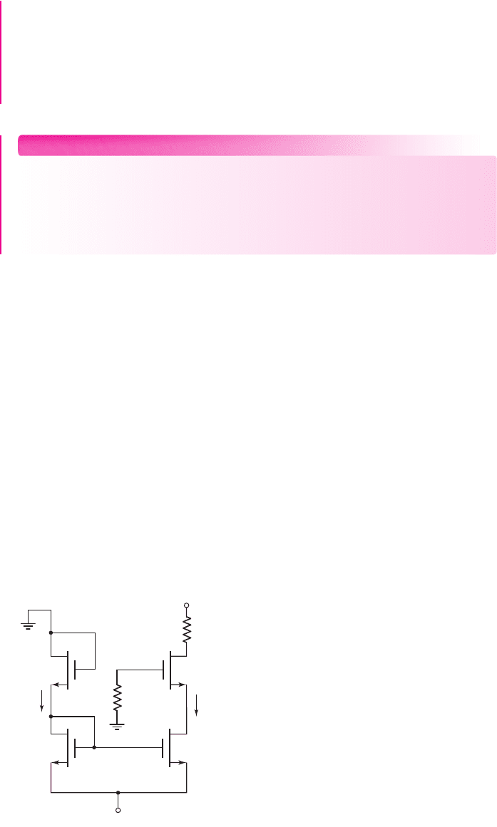
The constant-current source can be implemented by using MOSFETs as shown
in Figure 3.50. The transistors M
2
, M
3
, and M
4
form the current source. Transistors
M
3
and M
4
are each connected in a diode-type configuration, and they establish a ref-
erence current. We noted in the last section that this diode-type connection implies
the transistor is always biased in the saturation region. Transistors M
3
and M
4
are
therefore biased in the saturation region, and M
2
is assumed to be biased in the satu-
ration region. The resulting gate-to-source voltage on M
3
is applied to M
2
, and this
establishes the bias current I
Q
.
Since the reference current is the same in transistors M
3
and M
4
, we can write
K
n3
(V
GS3
− V
TN3
)
2
= K
n4
(V
GS4
− V
TN4
)
2
(3.28)
We also know that
V
GS4
+ V
GS3
= (−V
−
)
(3.29)
V
+
= 5 V
V
–
= –5 V
R
G
R
D
M
3
M
1
M
4
I
REF
I
Q
+
–
+
+
+
–
–
–
V
DS1
M
2
V
DS2
V
GS1
++++
–
–
V
GS2
V
GS3
V
GS4
Figure 3.50 Implementation of a MOSFET constant-current source
nea80644_ch03_125-204.qxd 06/08/2009 08:37 PM Page 173 F506 Hard disk:Desktop Folder:MHDQ134-03:

174 Part 1 Semiconductor Devices and Basic Applications
Solving Equation (3.29) for
V
GS4
and substituting the result into Equation (3.28)
yields
V
GS3
=
K
n4
K
n3
[(−V
−
) − V
TN4
] + V
TN3
1 +
K
n4
K
n3
(3.30)
Since
V
GS3
= V
GS2
, the bias current is
I
Q
= K
n2
(V
GS3
− V
TN2
)
2
(3.31)
EXAMPLE 3.16
Objective: Determine the currents and voltages in a MOSFET constant-current
source.
For the circuit shown in Figure 3.50, the transistor parameters are:
K
n1
=
0.2 mA/V
2
,
K
n2
= K
n3
= K
n4
= 0.1
mA/V
2
, and
V
TN1
= V
TN2
= V
TN3
= V
TN4
=
1V.
Solution: From Equation (3.30), we can determine
V
GS3
, as follows:
V
GS3
=
0.1
0.1
[5 − 1] +1
1 +
0.1
0.1
= 2.5V
Since M
3
and M
4
are identical transistors,
V
GS3
should be one-half of the bias volt-
age. The bias current I
Q
is then
I
Q
= (0.1) · (2.5 −1)
2
= 0.225 mA
The gate-to-source voltage on M
1
is found from
I
Q
= K
n1
(V
GS1
− V
TN1
)
2
or
0.225 = (0.2) · (V
GS1
−1)
2
which yields
V
GS1
= 2.06 V
The drain-to-source voltage on M
2
is
V
DS2
= (−V
−
) − V
GS1
= 5 −2.06 = 2.94 V
Since
V
DS2
= 2.94 V > V
DS
(sat) = V
GS2
− V
TN2
= 2.5 −1 = 1.5V
,
M
2
is biased
in the saturation region.
Design Consideration: Since in this example
M
2
and
M
3
are identical transistors,
the reference current I
REF
and bias current
I
Q
are equal. By redesigning the width-to-
length ratios of
M
2
,
M
3
, and
M
4
, we can obtain a specific bias current
I
Q
. If
M
2
and
nea80644_ch03_125-204.qxd 06/08/2009 08:37 PM Page 174 F506 Hard disk:Desktop Folder:MHDQ134-03:

Chapter 3 The Field-Effect Transistor 175
M
3
are not identical, then
I
Q
and
I
REF
will not be equal. A variety of design options
are possible with such a circuit configuration.
EXERCISE PROBLEM
Ex 3.16: Consider the constant-current source shown in Figure 3.50. Assume
that the threshold voltage of each transistor is
V
TN
= 1
V. (a) Design the ratio
of
K
n4
/K
n3
such that
V
GS3
= 2
V. (b) Determine
K
n2
such that
I
Q
= 100 μ
A.
(c) Find
K
n3
and
K
n4
such that
I
REF
= 200 μ
A. (Ans. (a)
K
n4
/K
n3
=
1
4
(b)
K
n2
= 0.1
mA/V
2
(c)
K
n3
= 0.2
mA/V
2
,
K
n4
= 0.05
mA/V
2
)
Test Your Understanding
TYU 3.15 Consider the circuit in Figure 3.49(b). Assume circuit parameters of
I
REF2
= 40 μ
A,
V
+
= 2.5
V,
V
−
=−2.5
V, and
R
D
= 20
k
. The transistor para-
meters are
V
TP
=−0.30
V,
K
pC
= 40 μ
A/V
2
,
K
pB
= 60 μ
A/V
2
, and
K
pA
=
75 μ
A/V
2
. Determine
I
Q2
and all source-to-gate voltages. (Ans.
I
Q2
= 60 μ
A,
V
SGC
= V
SGB
= 1.30
V,
V
SGA
= 1.19
V)
TYU 3.16 Consider the circuit shown in Figure 3.50. Assume all transistor threshold
voltages are 0.7 V. Determine the values of
K
n1
,
K
n2
,
K
n3
, and
K
n4
such that
I
REF
= 80 μ
A,
I
Q
= 120 μA
,
V
GS3
= 2
V, and
V
GS1
= 1.5
V. (Ans.
K
n1
= 187.5
μ
A/V
2
,
K
n2
= 71.0 μ
A/V
2
,
K
n3
= 47.3 μ
A/V
2
,
K
n4
= 15.12 μ
A/V
2
)
3.5 MULTISTAGE MOSFET CIRCUITS
Objective: • Consider the dc biasing of multistage or multitransistor
circuits.
In most applications, a single-transistor amplifier will not be able to meet the
combined specifications of a given amplification factor, input resistance, and output
resistance. For example, the required voltage gain may exceed that which can be
obtained in a single-transistor circuit.
Transistor amplifier circuits can be connected in series, or cascaded, as shown
in Figure 3.51. This may be done either to increase the overall small-signal voltage
gain, or provide an overall voltage gain greater than 1, with a very low output resistance.
+
–
v
i
R
i1
R
o1
R
i2
R
o2
+
–
v
o
Stage 1
A
V1
Stage 2
A
V2
Figure 3.51 Generalized two-stage amplifier
nea80644_ch03_125-204.qxd 06/08/2009 08:37 PM Page 175 F506 Hard disk:Desktop Folder:MHDQ134-03:
176 Part 1 Semiconductor Devices and Basic Applications
The overall voltage gain may not simply be the product of the individual amplifica-
tion factors. Loading effects, in general, need to be taken into account.
There are many possible multistage configurations; we will examine a few here,
in order to understand the type of analysis required.
Multitransistor Circuit: Cascade Configuration
The circuit shown in Figure 3.52 is a cascade of a common-source amplifier followed
by a source-follower amplifier. We will show in the next chapter that the common-
source amplifier provides a small-signal voltage gain and the source-follower has a
low output impedance.
3.5.1
R
2
v
i
R
1
C
C
C
S
R
D1
R
S1
R
S2
M
1
v
o
R
L
= 4 kΩ
C
C2
V
+
= 5 V
V
–
= –5 V
M
2
M
1
R
i
R
Si
R
o
+
–
Figure 3.52 Common-source amplifier in cascade with source follower
DESIGN EXAMPLE 3.17
Objective: Design the biasing of a multistage MOSFET circuit to meet specific
requirements.
Consider the circuit shown in Figure 3.52 with transistor parameters
K
n1
= 500 μ
A/V
2
,
K
n2
= 200 μ
A/V
2
,
V
TN1
= V
TN2
= 1.2
V, and
λ
1
= λ
2
= 0
.
Design the circuit such that
I
DQ1
= 0.2
mA,
I
DQ2
= 0.5
mA,
V
DSQ1
= V
DSQ2
=
6V
, and
R
i
= 100
k
. Let
R
Si
= 4
k
.
Solution: For output transistor M
2
, we have
V
DSQ2
= 5 −(−5) − I
DQ2
R
S2
or
6 = 10 −(0.5)R
S2
which yields
R
S2
= 8k
. Also, assuming transistors are biased in the saturation
region,
I
DQ2
= K
n2
(K
GS2
− V
TN2
)
2
or
0.5 = 0.2(V
GS2
−1.2)
2
nea80644_ch03_125-204.qxd 06/08/2009 08:37 PM Page 176 F506 Hard disk:Desktop Folder:MHDQ134-03:

Chapter 3 The Field-Effect Transistor 177
which yields
V
GS2
= 2.78 V
Since
V
DSQ2
= 6
V, the source voltage of
M
2
is
V
S2
=−1V
. With
V
GS2
=
2.78 V
, the gate voltage on
M
2
must be
V
G2
=−1 + 2.78 = 1.78 V
The resistor
R
D1
is then
R
D1
=
5 − 1.78
0.2
= 16.1k
For
V
DSQ1
= 6
V, the source voltage of
M
1
is
V
S1
= 1.78 −6 =−4.22 V
The resistor
R
S1
is then
R
S1
=
−4.22 − (−5)
0.2
= 3.9k
For transistor
M
1
, we have
I
DQ1
= K
n1
(V
GS1
− V
TN1
)
2
or
0.2 = 0.50(V
GS1
−1.2)
2
which yields
V
GS1
= 1.83 V
To find
R
1
and
R
2
, we can write
V
GS1
=
R
2
R
1
+ R
2
(10) − I
DQ1
R
S1
Since
R
2
R
1
+ R
2
=
1
R
1
·
R
1
R
2
R
1
+ R
2
=
1
R
1
· R
i
then, since the input resistance is specified to be 100 k
, we have
1.83 =
1
R
1
(100)(10) − (0.2)(3.9)
which yields
R
1
= 383
k
. From
R
i
= 100
k
, we find that
R
2
= 135
k
.
Comment: Both transistors are biased in the saturation region, as assumed, which is
desired for linear amplifiers as we will see in the next chapter.
EXERCISE PROBLEM
Ex 3.17: The transistor parameters for the circuit shown in Figure 3.52 are the
same as described in Example 3.17. Design the circuit such that
I
DQ1
= 0.1
mA,
I
DQ2
= 0.3
mA,
V
DSQ1
= V
DSQ2
= 5
V, and
R
i
= 200
k
. (Ans.
R
S2
=
16.7k
,
R
D1
= 25.8
k
,
R
S1
= 24.3
k
,
R
1
= 491
k
, and
R
2
= 337
k
)
nea80644_ch03_125-204.qxd 06/08/2009 08:37 PM Page 177 F506 Hard disk:Desktop Folder:MHDQ134-03: