Neamen D. Microelectronics: Circuit Analysis and Design
Подождите немного. Документ загружается.

198 Part 1 Semiconductor Devices and Basic Applications
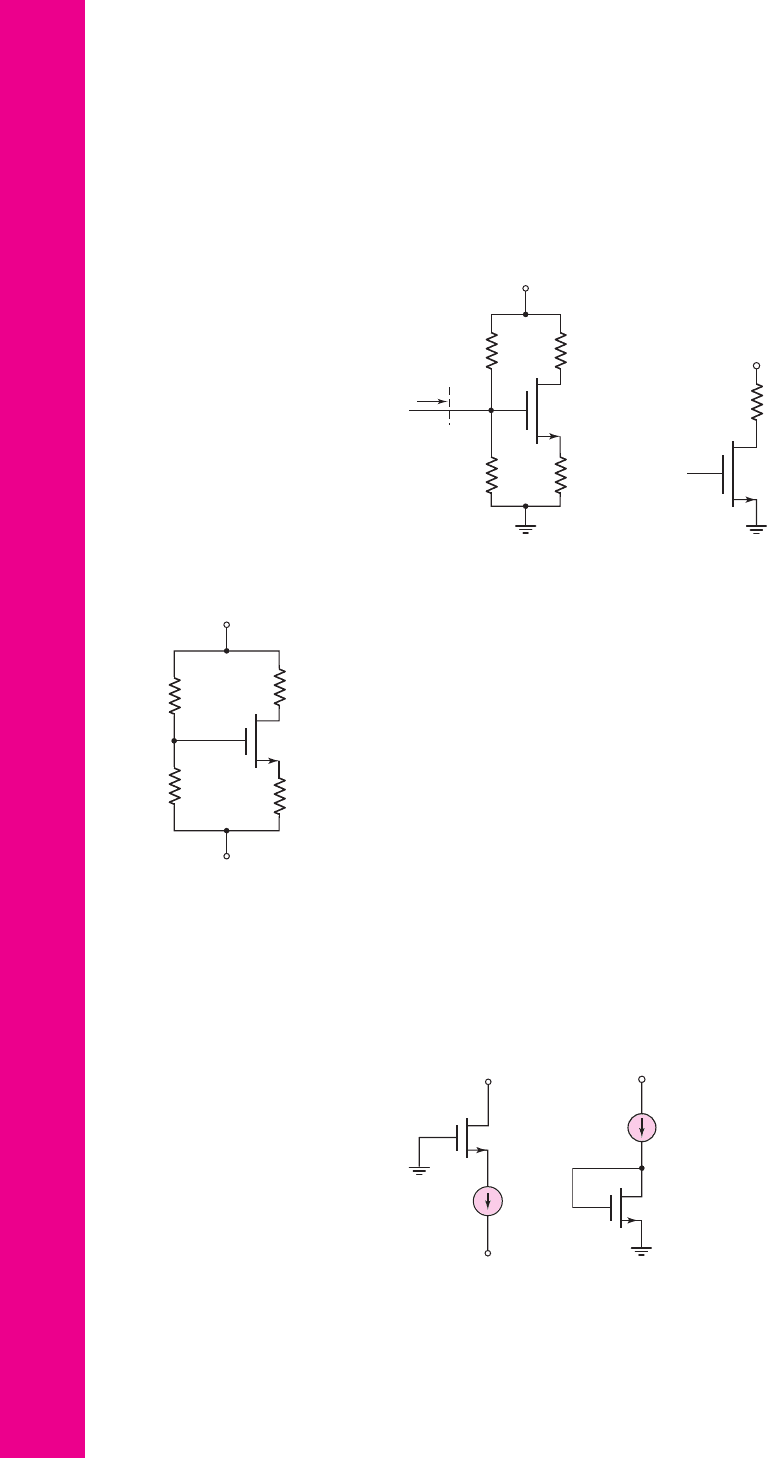
3.33 Consider the circuit shown in Figure P3.33. The transistor parameters are
V
TN
= 0.4
V and
k
n
= 120 μ
A/V
2
. The voltage drop across
R
S
is to be
0.20 V. Design the transistor
W/L
ratio such that
V
DS
= V
DS
(
sat
)
+0.4
V,
and determine
R
1
and
R
2
such that
R
in
= 200
k
.
V
DD
= 1.8 V
R
D
=
4 kΩ
R
S
=
1 kΩ
R
1
R
2
R
in
V
DD
= 1.8 V
R
D
=
2 kΩ
V
GS
Figure P3.33 Figure P3.34
3.34 The transistor parameters for the transistor in Figure P3.34 are
V
TN
= 0.4
V,
k
n
= 120 μ
A/V
2
, and
W/L = 50
. (a) Determine
V
GS
such
that
I
D
= 0.35
mA. (b) Determine
V
DS
and
V
DS
(
sat
)
.
3.35 For the transistor in the circuit in Figure P3.35, the parameters are
V
TN
= 0.4
V,
k
n
= 120 μ
A/V
2
, and
W/L = 25
. Determine
V
GS
,
I
D
, and
V
DS
. Sketch the load line and plot the
Q
-point.
D3.36 Design a MOSFET circuit with the configuration shown in Figure P3.30.
The transistor parameters are
V
TP
=−0.6
V,
k
p
= 50 μ
A/V
2
, and
λ = 0
.
The circuit bias is
±3
V, the drain current is to be 0.2 mA, the drain-to-
source voltage is to be approximately 3 V, and the voltage across
R
S
is to be
approximately equal to
V
SG
. In addition, the current through the bias resis-
tors is to be no more than 10 percent of the drain current. (Hint: choose a
reasonable value of width-to-length ratio for the transistor.)
3.37 The parameters of the transistors in Figures P3.37 (a) and (b) are
K
n
=
0.5 mA/V
2
,
V
TN
= 1.2V
, and
λ = 0
. Determine
v
GS
and
v
DS
for each tran-
sistor when (i)
I
Q
= 50 μA
and (ii)
I
Q
= 1mA
.
+5 V
–5 V
R
D
=
1.2 kΩ
R
S
=
0.5 kΩ
R
1
= 14 kΩ
R
2
= 6 kΩ
Figure P3.35
+5 V
−5 V
(a)
I
Q
+5 V
I
Q
(b)
Figure P3.37
nea80644_ch03_125-204.qxd 06/08/2009 08:37 PM Page 198 F506 Hard disk:Desktop Folder:MHDQ134-03:
Chapter 3 The Field-Effect Transistor 199
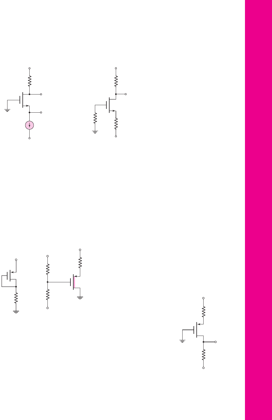
3.38 For the circuit in Figure P3.38, the transistor parameters are
V
TN
= 0.6V
and
K
n
= 200
μA/V
2
. Determine
V
S
and
V
D
.
*3.39 (a) Design the circuit in Figure P3.39 such that
I
DQ
= 0.50 mA
and
V
D
=
1 V. The transistor parameters are
K
n
= 0.25
mA/V
2
and
V
TN
= 1.4V
.
Sketch the load line and plot the Q-point. (b) Choose standard resistor
values that are closest to the ideal designed values. What are the resulting
Q-point values? (c) If the resistors in part (b) have tolerances of
±10
percent, determine the maximum and minimum values of
I
DQ
.
3.40 The PMOS transistor in Figure P3.40 has parameters
V
TP
=−0.7
V,
k
p
= 50 μ
A/V
2
,
L = 0.8 μ
m, and
λ = 0
. Determine the values of
W
and
R
such that
I
D
= 0.1
mA and
V
SD
= 2.5
V.
+9 V
−9 V
V
S
V
D
I
Q
= 0.25 mA
R
D
= 24 kΩ
Figure P3.38
+5 V
–5 V
V
D
R
D
R
G
= 47 kΩ
R
S
Figure P3.39
V
DD
= 9 V
R
Figure P3.40
+5 V
+5 V
–5 V
R
1
R
S
= 2 kΩ
R
2
Figure P3.41
3.41 Design the circuit in Figure P3.41 so that
V
SD
= 2.5V
. The current in the
bias resistors should be no more than 10 percent of the drain current. The
transistor parameters are
V
TP
=+1.5V
and
K
p
= 0.5
mA/V
2
.
*3.42 (a) Design the circuit in Figure P3.42 such that
I
DQ
= 0.25 mA
and
V
D
=−2
V. The nominal transistor parameters are
V
TP
=−1.2V
,
k
p
=
35 μ
A/V
2
, and
W/L = 15
. Sketch the load line and plot the Q-point.
(b) Determine the maximum and minimum Q-point values if the tolerance
of the
k
p
parameter is
±5
percent.
+5 V
–5 V
R
D
R
S
V
D
Figure P3.42
nea80644_ch03_125-204.qxd 06/08/2009 08:37 PM Page 199 F506 Hard disk:Desktop Folder:MHDQ134-03:
200 Part 1 Semiconductor Devices and Basic Applications
3.43 The parameters of the transistor in the circuit in Figure P3.43 are
V
TP
=
−1.75 V and
K
p
= 3
mA/V
2
. Design the circuit such that
I
D
= 5mA
,
V
SD
= 6V
, and
R
in
= 80 k
.
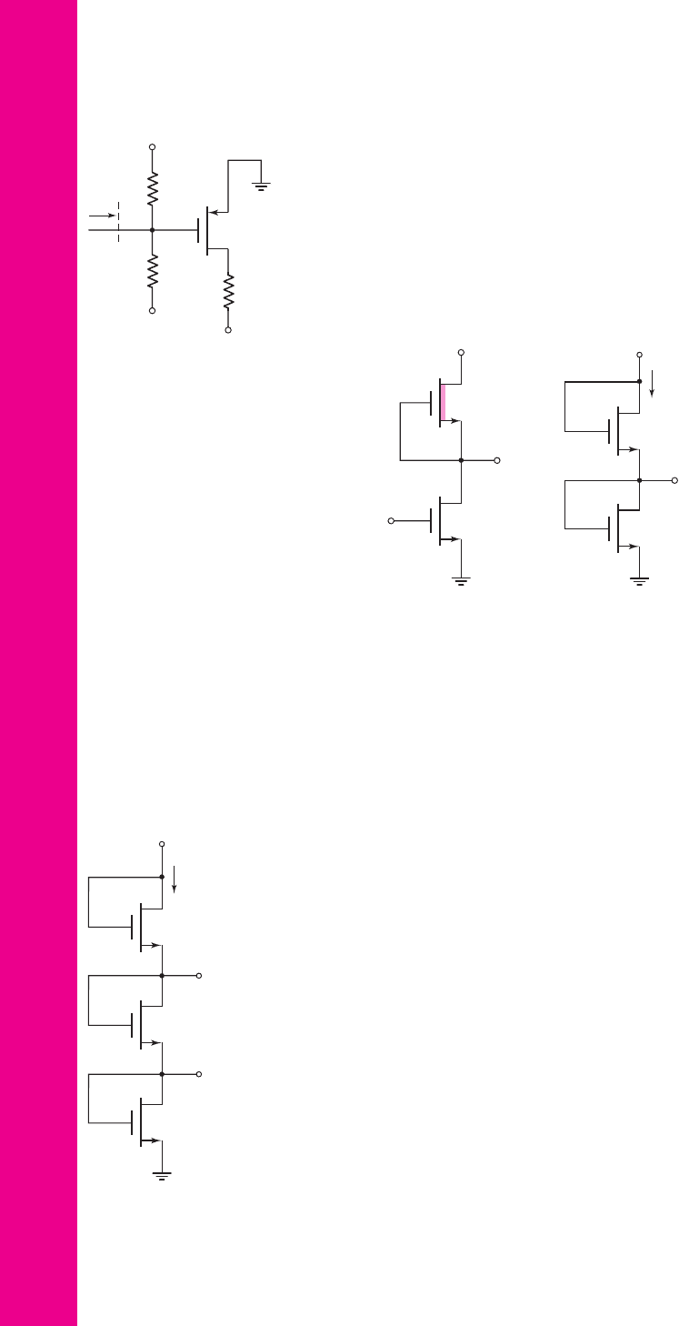
3.44 For each transistor in the circuit in Figure P3.44,
k
n
= 120 μ
A/V
2
. Also for
M
1
,
W/L = 4
and
V
TN
= 0.4
V, and for
M
2
,
W/L = 1
and
V
TN
=−0.6
V.
(a) Determine the input voltage such that both
M
1
and
M
2
are biased in the
saturation region. (b) Determine the region of operation of each transistor
and the output voltage
v
O
for: (i)
v
I
= 0.6
V and (ii)
v
I
= 1.5
V.
+5 V
–10 V
–5 V
R
D
R
1
R
2
R
in
Figure P3.43
V
DD
= 5 V
v
O
v
I
M
2
M
1
Figure P3.44
V
DD
= 5 V
V
O
M
2
M
1
I
D
Figure P3.46
3.45 Consider the circuit in Figure P3.44. The transistor parameters for
M
1
are
V
TN
= 0.4
V and
k
n
= 120 μ
A/V
2
, and for
M
2
are
V
TN
=−0.6
V,
k
n
= 120 μ
A/V
2
, and
W/L = 1
. Determine the
W/L
ratio of
M
1
such that
v
O
= 0.025
V when
v
I
= 3
V.
3.46 The transistors in the circuit in Figure P3.46 both have parameters
V
TN
= 0.4
V and
k
n
= 120 μ
A/V
2
. (a) If the width-to-length ratios of
M
1
and
M
2
are
(W/L)
1
= (W/L)
2
= 30
, determine
V
GS1
,
V
GS2
,
V
O
, and
I
D
.
(b) Repeat part (a) if the width-to-length ratios are changed to
(W/L)
1
= 30
and
(W/L)
2
= 15
. (c) Repeat part (a) if the width-to-length ratios are
changed to
(W/L)
1
= 15
and
(W/L)
2
= 30
.
3.47 Consider the circuit in Figure P3.47. (a) The nominal transistor parameters
are
V
TN
= 0.6
V and
k
n
= 120 μ
A/V
2
. Design the width-to-length ratio re-
quired in each transistor such that
I
DQ
= 0.8
mA,
V
1
= 2.5
V, and
V
2
= 6
V. (b) Determine the change in the values of
V
1
and
V
2
if the
k
n
pa-
rameter in each transistor changes by (i)
+5
percent and (ii)
−5
percent.
(c) Determine the values of
V
1
and
V
2
if the
k
n
parameter of
M
1
decreases
by 5 percent and the
k
n
parameter of
M
2
and
M
3
increases by 5 percent.
3.48 The transistors in the circuit in Figure 3.36 in the text have parameters
V
TN
= 0.6
V,
k
n
= 120 μ
A/V
2
, and
λ = 0
. The width-to-length ratio of
M
L
is
(W/L)
L
= 2
. Design the width-to-length ratio of the driver transistor
such that
V
O
= 0.15
V when
V
I
= 5V
.
3.49 For the circuit in Figure 3.39 in the text, the transistor parameters are:
V
TND
= 0.6
V,
V
TNL
=−1.2
V,
λ = 0
, and
k
n
= 120 μ
A/V
2
. Let
V
DD
= 5
V. The width-to-length ratio of
M
L
is
(W/L)
L
= 2
. Design the
width-to-length ratio of the driver transistor such that
V
O
= 0.10
V when
V
I
= 5
V.
V
DD
= 9 V
V
2
M
2
V
1
M
3
M
1
I
D
Figure P3.47
nea80644_ch03_125-204.qxd 06/08/2009 08:37 PM Page 200 F506 Hard disk:Desktop Folder:MHDQ134-03:
Chapter 3 The Field-Effect Transistor 201
Section 3.3 MOSFET Switch and Amplifier
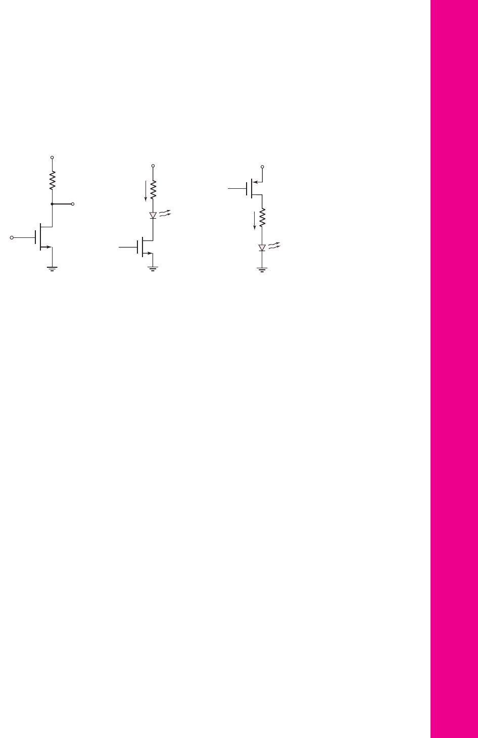
3.50 Consider the circuit in Figure P3.50. The circuit parameters are
V
DD
= 3
V
and
R
D
= 30
k
. The transistor parameters are
V
TN
= 0.4
V and
k
n
= 120 μ
A/V
2
. (a) Determine the transistor width-to-length ratio such
that
V
O
= 0.08
V when
V
I
= 2.6
V. (b) Repeat part (a) for
V
I
= 3
V.
V
DD
V
O
V
I
R
D
Figure P3.50
R
D
Light
outpu
t
I
D
V
I
+5 V
Figure P3.51
V
I
R
D
I
D
Light
LED
outpu
t
+5 V
Figure P3.52
3.51 The transistor in the circuit in Figure P3.51 is used to turn the LED on and
off. The transistor parameters are
V
TN
= 0.6
V,
k
n
= 80 μ
A/V
2
, and
λ = 0
.
The diode cut-in voltage is
V
γ
= 1.6
V. Design
R
D
and the transistor width-
to-length ratio such that
I
D
= 12
mA for
V
I
= 5
V and
V
DS
= 0.15
V.
3.52 The circuit in Figure P3.52 is another configuration used to switch an LED on
and off. The transistor parameters are
V
TP
=−0.6
V,
k
p
= 40 μ
A/V
2
, and
λ = 0
. The diode cut-in voltage is
V
γ
= 1.6
V. Design
R
D
and the transistor
width-to-length ratio such that
I
D
= 15
mA for
V
I
= 0
V and
V
SD
= 0.20
V.
3.53 For the two-input NMOS NOR logic gate in Figure 3.46 in the text, the tran-
sistor parameters are
V
TN1
= V
TN2
= 0.6
V,
λ
1
= λ
2
= 0
, and
k
n1
= k
n2
=
120 μ
A/V
2
. The drain resistor is
R
D
= 50
k
. (a) Determine the width-to-
length ratios of the transistors so that
V
O
= 0.15 V
when
V
1
= V
2
= 5
V.
Assume that
(W/L)
1
= (W/L)
2
. (b) Using the results of part (a), find
V
O
when
V
1
= 5
V and
V
2
= 0.2
V.
3.54 All transistors in the current-source circuit shown in Figure 3.49(a) in the
text have parameters
V
TN
= 0.4
V,
k
n
= 120 μ
A/V
2
, and
λ = 0
. Transistors
M
1
and
M
2
are matched. The bias sources are
V
+
= 2.5
V and
V
−
=−2.5
V.
The currents are to be
I
Q1
= 125 μ
A and
I
REF1
= 225 μ
A. For
M
2
, we re-
quire
V
DS2
(
sat
)
= 0.5
V, and for
M
1
we require
V
DS1
= 2
V. (a) Find the
W/L
ratios of the transistors. (b) Find
R
D
.
3.55 All transistors in the current-source circuit shown in Figure 3.49(b) in the
text have parameters
V
TP
=−0.4
V,
k
p
= 50 μ
A/V
2
, and
λ = 0
. The bias
sources are
V
+
= 5V
and
V
−
=−5V
. The currents are to be
I
Q2
= 200 μ
A and
I
REF2
= 125 μA
. For
M
B
, we require
V
SDB
(sat) = 0.8V
,
and for
M
A
, we require
V
SDA
= 4
V. Transistors
M
A
and
M
B
are matched.
(a) Find the
W/L
ratios of the transistors. (b) Find the value of
R
D
.
3.56 Consider the circuit shown in Figure 3.50 in the text. The threshold voltage
and process conduction parameter for each transistor is
V
TN
= 0.6
V and
k
n
= 120 μ
A/V
2
. Let
λ = 0
for all transistors. Assume that
M
1
and
M
2
are
matched. Design width-to-length ratios such that
I
Q
= 0.35
mA,
I
REF
= 0.15
mA, and
V
DS2
(
sat
)
= 0.5
V. Find
R
D
such that
V
DS1
= 3.5
V.
nea80644_ch03_125-204.qxd 06/08/2009 08:37 PM Page 201 F506 Hard disk:Desktop Folder:MHDQ134-03:
202 Part 1 Semiconductor Devices and Basic Applications
Section 3.6 Junction Field-Effect Transistor
3.57 The gate and source of an n-channel depletion-mode JFET are connected
together. What value of V
DS
will ensure that this two-terminal device is
biased in the saturation region. What is the drain current for this bias
condition?
3.58 For an n-channel JFET, the parameters are
I
DSS
= 6
mA and
V
P
=−3
V.
Calculate V
DS
(sat). If
V
DS
> V
DS
(sat), determine I
D
for: (a) V
GS
= 0,
(b)
V
GS
=−1
V, (c)
V
GS
=−2
V, and (d)
V
GS
=−3
V.
3.59 A p-channel JFET biased in the saturation region with V
SD
=5 V has a drain
current of
I
D
= 2.8
mA at
V
GS
= 1
V and
I
D
= 0.30
mA at
V
GS
= 3
V.
Determine I
DSS
and V
P
.
3.60 Consider the p-channel JFET in Figure P3.60. Determine the range of V
DD
that will bias the transistor in the saturation region. If
I
DSS
= 6
mA and
V
P
= 2.5
V, find V
S
.
3.61 Consider a GaAs MESFET. When the device is biased in the saturation re-
gion, we find that
I
D
= 18.5
μA at
V
GS
= 0.35
V and
I
D
= 86.2
μA at
V
GS
= 0.50
V. Determine the conduction parameter k and the threshold
voltage V
TN
.
3.62 The threshold voltage of a GaAs MESFET is
V
TN
= 0.24
V. The maximum
allowable gate-to-source voltage is V
GS
= 0.75 V. When the transistor is bi-
ased in the saturation region, the maximum drain current is
I
D
= 250
μA.
What is the value of the conduction parameter k?
*3.63 For the transistor in the circuit in Figure P3.63, the parameters are:
I
DSS
=
10 mA and
V
P
=−5
V. Determine I
DQ
, V
GSQ
, and V
DSQ
.
3.64 Consider the source follower with the n-channel JFET in Figure P3.64. The
input resistance is to be R
in
=500 k
. We wish to have I
DQ
=5 mA, V
DSQ
=
8 V, and
V
GSQ
=−1
V. Determine R
S
, R
1
, and R
2
, and the required transis-
tor values of I
DSS
and V
P
.
3.65 The transistor in the circuit in Figure P3.65 has parameters
I
DSS
= 8
mA
and
V
P
= 4
V. Design the circuit such that
I
D
= 5
mA. Assume R
in
=
100 k
. Determine V
GS
and V
SD
.
3.66 For the circuit in Figure P3.66, the transistor parameters are I
DSS
= 7 mA
and V
P
= 3 V. Let R
1
+ R
2
= 100 k
. Design the circuit such that I
DQ
=
5.0 mA and V
SDQ
= 6 V.
V
DD
V
S
I
Q
= 2 mA
V
+
Figure P3.60
V
DD
= 20 V
R
G
= 50 kΩ
R
S
= 0.2 kΩ
v
i
R
D
= 2 kΩ
+
–
C
C
Figure P3.63
R
S
R
1
R
in
V
DD
= 10 V
R
2
Figure P3.64
R
D
= 2 kΩ
R
1
R
in
V
DD
= 20 V
R
2
R
S
= 0.5 kΩ
Figure P3.65
R
D
R
1
V
DD
= 12 V
R
2
R
S
= 0.3 kΩ
Figure P3.66
nea80644_ch03_125-204.qxd 06/08/2009 08:37 PM Page 202 F506 Hard disk:Desktop Folder:MHDQ134-03:
Chapter 3 The Field-Effect Transistor 203
3.67 The transistor in the circuit in Figure P3.67 has parameters I
DSS
=8 mA and
V
P
=−4
V. Determine V
G
, I
DQ
, V
GSQ
, and V
DSQ
.
3.68 Consider the circuit in Figure P3.68. The quiescent value of V
DS
is found to
be V
DSQ
= 5 V. If I
DSS
= 10 mA, determine I
DQ
, V
GSQ
, and V
P
.
3.69 For the circuit in Figure P3.69, the transistor parameters are I
DSS
= 4 mA
and
V
P
=−3
V. Design R
D
such that
V
DS
=|V
P
|
. What is the value of I
D
?
3.70 Consider the source-follower circuit in Figure P3.70. The transistor para-
meters are I
DSS
= 2 mA and V
P
= 2 V. Design the circuit such that I
DQ
=
1 mA, V
SDQ
= 10 V, and the current through R
1
and R
2
is 0.1 mA.
3.71 The GaAs MESFET in the circuit in Figure P3.71 has parameters k =
250 μA/V
2
and V
TN
= 0.20 V. Let R
1
+ R
2
= 150 k
. Design the circuit
such that
I
D
= 40
μA and V
DS
= 2 V.
3.72 For the circuit in Figure P3.72, the GaAs MESFET threshold voltage is
V
TN
= 0.15
V. Let
R
D
= 50
k
. Determine the value of the conduction pa-
rameter required so that
V
O
= 0.70
V when
V
I
= 0.75
V.
COMPUTER SIMULATION PROBLEMS
3.73 Using a computer simulation, verify the results of Exercise Ex 3.5.
3.74 (a) Using a computer simulation, plot the voltage transfer characteristics of
the CMOS circuit shown in Figure 3.41. Use the parameters given in Ex-
ample 3.11. (b) Repeat part (a) for the case when the width-to-length ratio
of
M
N
is doubled.
3.75 (a) Using a computer simulation, plot the voltage transfer characteristics of
the NMOS circuit shown in Figure 3.46 for
V
2
= 0
and
0 ≤ V
1
≤ 5
V. Use
the circuit and transistor parameters given in Example 3.13. (b) Repeat part
(a) for
0 ≤ V
1
= V
2
≤ 5
V.
3.76 Using a computer simulation, verify the results of Example 3.17 for the
multitransistor circuit shown in Figure 3.52.
R
S
= 2 kΩ
R
1
= 140 kΩ
V
DD
= 20 V
R
2
= 60 kΩ
R
D
= 2.7 kΩ
Figure P3.67
V
DD
= 12 V
v
o
R
2
=
20 kΩ
R
L
= 2 kΩ
R
S
=
0.5 kΩ
v
i
R
D
= 1 kΩ
R
1
= 450 kΩ
+
–
C
C1
R
in
C
C2
Figure P3.68
V
DD
= 10 V
R
D
Figure P3.69
R
1
V
DD
= 20 V
R
2
R
S
Figure P3.70
R
1
V
DD
= 3 V
R
2
R
D
R
S
= 10 kΩ
Figure P3.71
V
DD
= 3 V
V
O
V
I
R
D
Figure P3.72
nea80644_ch03_125-204.qxd 06/10/2009 07:53 PM Page 203 F506 Tempwork:Dont' Del Rakesh:June:Rakesh 06-10-09:MHDQ134-03:

204 Part 1 Semiconductor Devices and Basic Applications
DESIGN PROBLEMS
[Note: All design should be correlated with a computer simulation.]
*D3.77 Consider the PMOS circuit shown in Figure 3.30. The circuit is to be re-
designed such that
I
DQ
= 100 μ
A and the Q-point is in the center of the sat-
uration region of the load line. Assume
R
1
+ R
2
= 500
k
and assume the
same transistor parameters as given in Exercise Ex 3.6.
*D3.78 Consider the circuit in Figure 3.39 with a depletion load. Assume the circuit
is biased at
V
DD
= 3.3
V, and assume transistor threshold voltages of
V
TND
= 0.4
V and
V
TNL
=−0.75
V. Also assume
k
n
= 80 μ
A/V
2
. Design
the circuit such that
V
O
= 0.05
V when
V
I
= 3.3
V and that the maximum
power dissipation is
150 μ
W.
*D3.79 The constant-current source in Figure 3.50 is to be redesigned. The bias
voltages are
V
+
= 3.3
V and
V
−
=−3.3
V. The parameters of all transis-
tors are
V
TN
= 0.4
V and
k
n
= 100 μ
A/V
2
. The currents are to be
I
REF
= 100 μ
A and
I
Q
= 60 μ
A. We will also specify that
V
DS2
(
sat
)
=
0.6
V,
V
GS1
= V
GS2
, and
V
DS1
= 2.5
V. Determine all width-to-length ratios
and the value of
R
D
. (Note: the minimum width-to-length ratio is to be
greater than one.)
*D3.80 Consider the multitransistor circuit in Figure 3.52. The bias voltages are
changed to
V
+
= 3.3
V and
V
−
=−3.3
V. The transistor parameters are
V
TN
= 0.4
V and
k
n
= 100 μ
A/V
2
. Design the circuit such that
I
DQ1
=
100 μ
A,
I
DQ2
= 250 μ
A,
V
DSQ1
= V
DSQ2
= 3.3
V, and
R
i
= 200
k
.
nea80644_ch03_125-204.qxd 06/08/2009 08:37 PM Page 204 F506 Hard disk:Desktop Folder:MHDQ134-03:

Chapter
In Chapter 3, we described the structure and operation of the FET, in particular the
MOSFET, and analyzed and designed the dc response of circuits containing these
devices. In this chapter, we emphasize the use of the FETs in linear amplifier appli-
cations. Linear amplifiers imply that, for the most part, we are dealing with analog
signals. The magnitude of an analog signal may have any value, within limits, and
may vary continuously with respect to time. Although a major use of MOSFETs is in
digital applications, they are also used in linear amplifier circuits.
We will begin to see how all-transistor circuits, that is, circuits with no resistors,
can be designed. Since MOS transistors are small devices, high-density all-transistor
circuits can be fabricated as integrated circuits.
PREVIEW
In this chapter, we will:
• Investigate the process by which a single-MOS transistor circuit can amplify
a small, time-varying input signal.
• Develop the small-signal models of the transistor that are used in the analysis
of linear amplifiers.
• Discuss the three basic transistor amplifier configurations.
• Analyze the common-source, source-follower, and common-gate amplifiers,
and become familiar with the general characteristics of these circuits.
• Compare the general characteristics of the three basic amplifier
configurations.
• Analyze all-MOS transistor circuits that become the foundation of integrated
circuits.
• Analyze multitransistor or multistage amplifiers and understand the advan-
tages of these circuits over single-transistor amplifiers.
• Develop the small-signal model of JFET devices and analyze basic JFET
amplifiers.
• As an application, incorporate MOS transistors in a design of a two-stage
amplifier.
4
4
Basic FET Amplifiers
205
nea80644_ch04_205-284.qxd 06/12/2009 08:00 PM Page 205 F506 Tempwork:Dont' Del Rakesh:June:Rakesh 06-12-09:MHDQ134-04:
206 Part 1 Semiconductor Devices and Basic Applications
4.1 THE MOSFET AMPLIFIER
Objective: • Investigate the process by which a single-transistor
circuit can amplify a small, time-varying input signal and develop the
small-signal models of the transistor that are used in the analysis of
linear amplifiers.
In this chapter, we will be considering signals, analog circuits, and amplifiers. A
signal contains some type of information. For example, sound waves produced by a
speaking human contain the information the person is conveying to another person.
A sound wave is an analog signal. The magnitude of an analog signal can take on
any value, within limits, and may vary continuously with time. Electronic circuits
that process analog signals are called analog circuits. One example of an analog cir-
cuit is a linear amplifier. A linear amplifier magnifies an input signal and produces
an output signal whose magnitude is larger and directly proportional to the input
signal.
In this chapter, we analyze and design linear amplifiers that use field-effect tran-
sistors as the amplifying device. The term small signal means that we can linearize
the ac equivalent circuit. We will define what is meant by small signal in the case of
MOSFET circuits. The term linear amplifiers means that we can use superposition so
that the dc analysis and ac analysis of the circuits can be performed separately and
the total response is the sum of the two individual responses.
The mechanism with which MOSFET circuits amplify small time-varying
signals was introduced in the last chapter. In this section, we will expand that
discussion using the graphical technique, dc load line, and ac load line. In the
process, we will develop the various small-signal parameters of linear circuits and
the corresponding equivalent circuits.
Graphical Analysis, Load Lines,
and Small-Signal Parameters
Figure 4.1 shows an NMOS common-source circuit with a time-varying voltage
source in series with the dc source. We assume the time-varying input signal is sinu-
soidal. Figure 4.2 shows the transistor characteristics, dc load line, and Q-point,
where the dc load line and Q-point are functions of
v
GS
,
V
DD
, R
D
, and the transistor
parameters. For the output voltage to be a linear function of the input voltage, the
transistor must be biased in the saturation region. (Note that, although we primarily
use n-channel, enhancement-mode MOSFETs in our discussions, the same results
apply to the other MOSFETs.)
Also shown in Figure 4.2 are the sinusoidal variations in the gate-to-source volt-
age, drain current, and drain-to-source voltage, as a result of the sinusoidal source v
i
.
The total gate-to-source voltage is the sum of
V
GSQ
and
v
i
. As
v
i
increases, the
instantaneous value of
v
GS
increases, and the bias point moves up the load line. A
larger value of
v
GS
means a larger drain current and a smaller value of
v
DS
. For a
negative
v
i
(the negative portion of the sine wave), the instantaneous value of
v
GS
decreases below the quiescent value, and the bias point moves down the load line. A
smaller
v
GS
value means a smaller drain current and increased value of
v
DS
. Once the
4.1.1
+
–
v
GS
R
D
v
i
i
D
v
O
+
–
v
DS
V
DD
+
–
V
GSQ
+
–
Figure 4.1 NMOS common-
source circuit with time-
varying signal source in
series with gate dc source
nea80644_ch04_205-284.qxd 06/12/2009 08:00 PM Page 206 F506 Tempwork:Dont' Del Rakesh:June:Rakesh 06-12-09:MHDQ134-04:
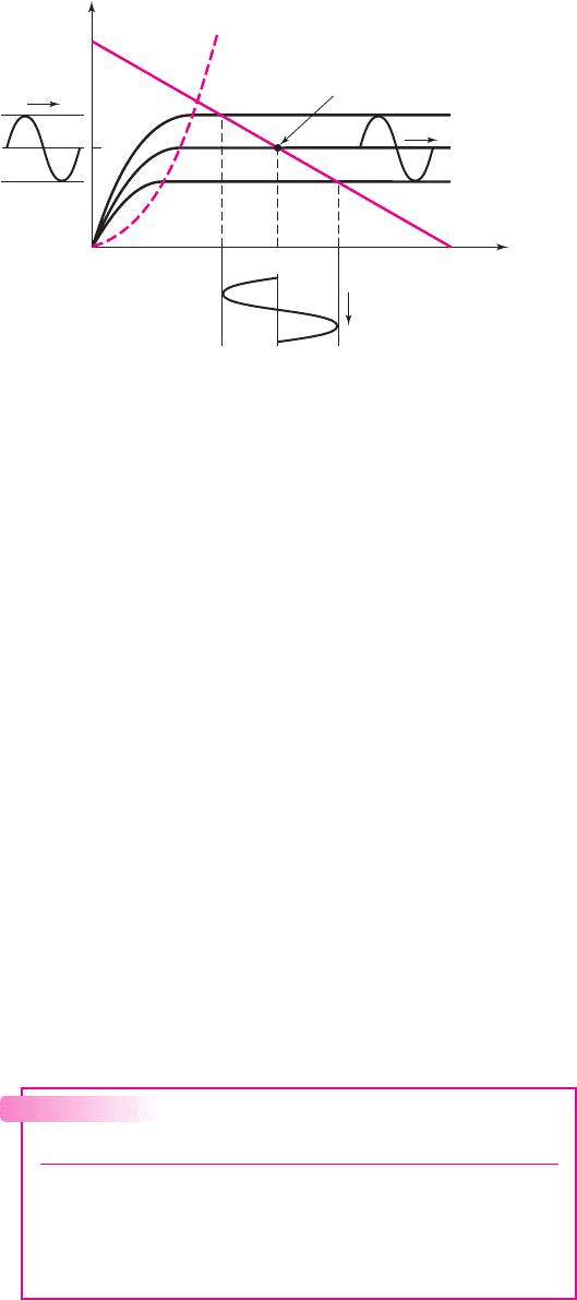
Chapter 4 Basic FET Amplifiers 207
v
D
S
I
DQ
v
i
V
DD
V
DSQ
V
GSQ
v
DS
(sat)
Time
Time
Time
i
D
Q-point
Figure 4.2 Common-source transistor characteristics, dc load line, and sinusoidal variation
in gate-to-source voltage, drain current, and drain-to-source voltage
Q-point is established, we can develop a mathematical model for the sinusoidal, or
small-signal, variations in gate-to-source voltage, drain-to-source voltage, and drain
current.
The time-varying signal source
v
i
in Figure 4.1 generates a time-varying
component of the gate-to-source voltage. In this case,
v
gs
= v
i
, where
v
gs
is the time-
varying component of the gate-to-source voltage. For the FET to operate as a linear
amplifier, the transistor must be biased in the saturation region, and the instantaneous
drain current and drain-to-source voltage must also be confined to the saturation
region.
When symmetrical sinusoidal signals are applied to the input of an amplifier,
symmetrical sinusoidal signals are generated at the output, as long as the amplifier
operation remains linear. We can use the load line to determine the maximum output
symmetrical swing. If the output exceeds this limit, a portion of the output signal will
be clipped and signal distortion will occur.
In the case of FET amplifiers, the output signal must avoid cutoff (
i
D
= 0
) and
must stay in the saturation region (
v
DS
>v
DS
(sat)). This maximum range of output
signal can be determined from the load line in Figure 4.2.
Transistor Parameters
We will be dealing with time-varying as well as dc currents and voltages in this
chapter. Table 4.1 gives a summary of notation that will be used. This notation was
Table 4.1 Summary of notation
Variable Meaning
i
D
, v
GS
Total instantaneous values
I
D
, V
GS
DC values
i
d
, v
gs
Instantaneous ac values
I
d
, V
gs
Phasor values
nea80644_ch04_205-284.qxd 06/12/2009 08:00 PM Page 207 F506 Tempwork:Dont' Del Rakesh:June:Rakesh 06-12-09:MHDQ134-04: