Neamen D. Microelectronics: Circuit Analysis and Design
Подождите немного. Документ загружается.


228 Part 1 Semiconductor Devices and Basic Applications
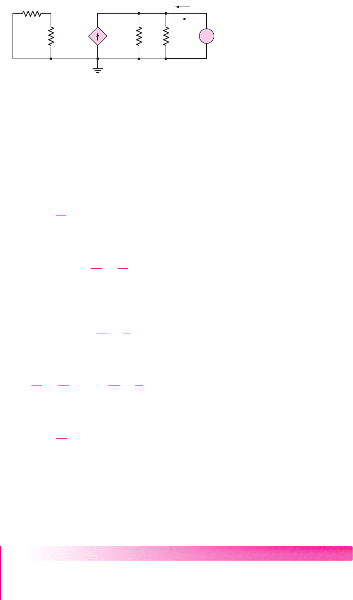
parallel with the dependent current source. Figure 4.27(b) is the same equivalent
circuit, but with all signal grounds at a common point. We are again neglecting the
body effect. The output voltage is
V
o
= (g
m
V
gs
)(R
S
r
o
)
(4.30)
Writing a KVL equation from input to output results in the following:
V
in
= V
gs
+ V
o
= V
gs
+ g
m
V
gs
(R
S
r
o
)
(4.31(a))
Therefore, the gate-to-source voltage is
V
gs
=
V
in
1 + g
m
(R
S
r
o
)
=
1
g
m
1
g
m
+(R
S
r
o
)
· V
in
(4.31(b))
Equation (4.31(b)) is written in the form of a voltage-divider equation, in which
the gate-to-source of the NMOS device looks like a resistance with a value of
1/g
m
.
More accurately, the effective resistance looking into the source terminal (ignoring
r
o
) is 1/g
m
. The voltage V
in
is related to the source input voltage V
i
by
V
in
=
R
i
R
i
+ R
Si
· V
i
(4.32)
where
R
i
= R
1
R
2
is the input resistance to the amplifier.
Substituting Equations (4.31(b)) and (4.32) into (4.30), we have the small-signal
voltage gain:
A
v
=
V
o
V
i
=
g
m
(R
S
r
o
)
1 + g
m
(R
S
r
o
)
·
R
i
R
i
+ R
Si
(4.33(a))
or
A
v
=
R
S
r
o
1
g
m
+ R
S
r
o
·
R
i
R
i
+ R
Si
(4.33(b))
which again is written in the form of a voltage-divider equation. An inspection of Equa-
tion 4.33(b) shows that the magnitude of the voltage gain is always less than unity.
EXAMPLE 4.7
Objective: Calculate the small-signal voltage gain of the source-follower circuit in
Figure 4.26.
Assume the circuit parameters are
V
DD
= 12
V,
R
1
= 162
k,
R
2
= 463
k,
and
R
S
= 0.75
k, and the transistor parameters are
V
TN
= 1.5
V,
K
n
= 4
mA/V
2
,
and
λ = 0.01 V
−1
.
Also assume
R
Si
= 4
k.
Solution: The dc analysis results are
I
DQ
= 7.97
mA and
V
GSQ
= 2.91
V. The
small-signal transconductance is therefore
g
m
= 2K
n
(V
GSQ
− V
TN
) = 2(4)(2.91 −1.5) = 11.3mA/V
and the small-signal transistor resistance is
r
o
∼
=
[λI
DQ
]
−1
= [(0.01)(7.97)]
−1
= 12.5k
The amplifier input resistance is
R
i
= R
1
R
2
= 162
463 = 120 k
nea80644_ch04_205-284.qxd 06/12/2009 08:00 PM Page 228 F506 Tempwork:Dont' Del Rakesh:June:Rakesh 06-12-09:MHDQ134-04:

Chapter 4 Basic FET Amplifiers 229
The small-signal voltage gain then becomes
A
v
=
g
m
(R
S
r
o
)
1 + g
m
(R
S
r
o
)
·
R
i
R
i
+ R
Si
=
(11.3)(0.75
12.5)
1 + (11.3)(0.75
12.5)
·
120
120 + 4
=+0.860
Comment: The magnitude of the small-signal voltage gain is less than 1. An exam-
ination of Equation (4.33(b)) shows that this is always true. Also, the voltage gain is
positive, which means that the output signal voltage is in phase with the input signal
voltage. Since the output signal is essentially equal to the input signal, the circuit is
called a source follower.
EXERCISE PROBLEM
Ex 4.7: The source-follower circuit in Figure 4.26 has transistor parameters
V
TN
=+0.8
V,
K
n
= 1
mA/V
2
, and
λ = 0.015 V
−1
. Let
V
DD
= 10
V,
R
Si
=
200
, and
R
1
+ R
2
= 400
k. Design the circuit such that
I
DQ
= 1.5
mA and
V
DSQ
= 5
V. Determine the small-signal voltage gain. (Ans.
R
S
= 3.33
k,
R
1
= 119
k,
R
2
= 281
,k,
A
v
= 0.884
)
Although the voltage gain is slightly less than 1, the source follower is an
extremely useful circuit because the output resistance is less than that of a common-
source circuit, as we will show in the next section. A small output resistance is
desirable when the circuit is to act as an ideal voltage source and drive a load circuit
without suffering any loading effects.
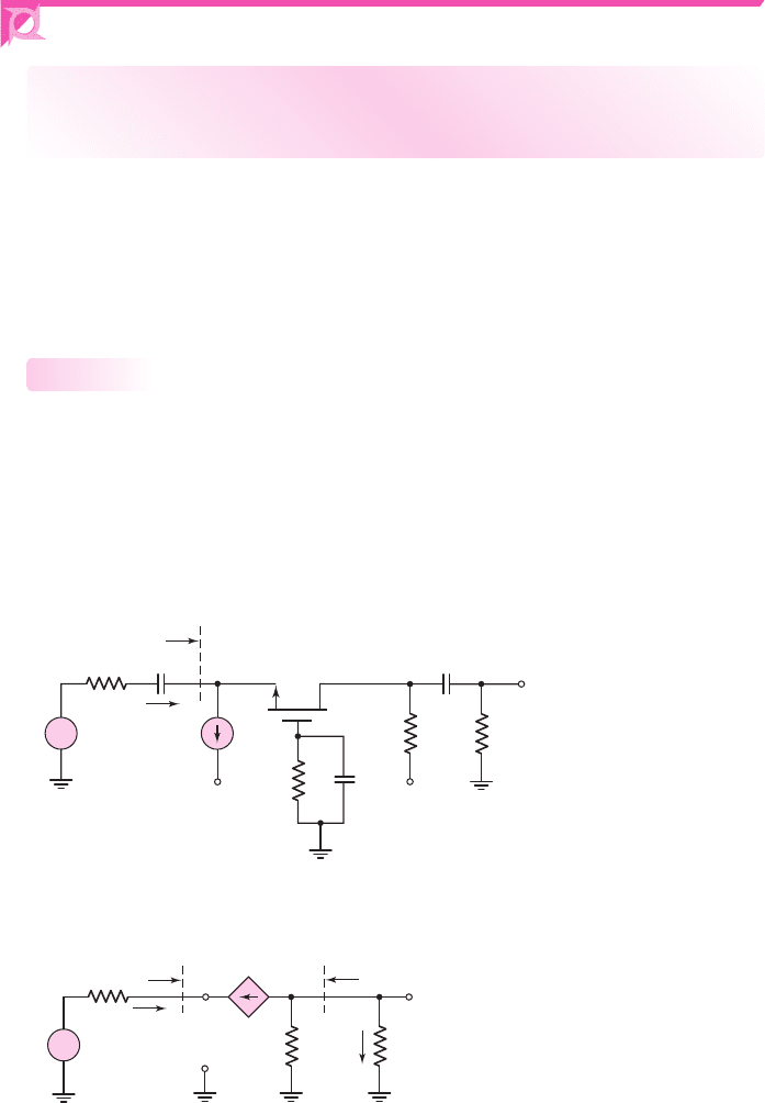
DESIGN EXAMPLE 4.8
Objective: Design a source-follower amplifier with a p-channel enhancement-mode
MOSFET to meet a set of specifications.
Specifications: The circuit to be designed has the configuration shown in Fig-
ure 4.28 with circuit parameters
V
DD
= 20
V and
R
Si
= 4
k. The Q-point values
are to be in the center of the load line with
I
DQ
= 2.5
mA. The input resistance is to
R
2
v
i
R
1
C
C1
R
S
V
DD
v
O
R
i
R
Si
+
–
Figure 4.28 PMOS source follower
nea80644_ch04_205-284.qxd 06/12/2009 08:00 PM Page 229 F506 Tempwork:Dont' Del Rakesh:June:Rakesh 06-12-09:MHDQ134-04:

230 Part 1 Semiconductor Devices and Basic Applications
be
R
i
= 200
k. The transistor
W/L
ratio is to be designed such that the small sig-
nal voltage gain is
A
v
= 0.90
.
Choices: A transistor with nominal parameters
V
TP
=−2
V,
k
p
= 40 μA/V
2
,
and
λ = 0
is available.
Solution (dc analysis): From a KVL equation around the source-to-drain loop, we have
V
DD
= V
SDQ
+ I
DQ
R
S
or
20 = 10 +(2.5)R
S
which yields the required source resistor to be
R
S
= 4
k.
Solution (ac design): The small-signal voltage gain of this circuit is the same as that
of a source follower with an NMOS device. From Equation (4.33(a)), we have
A
v
=
V
o
V
i
=
g
m
R
S
1 + g
m
R
S
·
R
i
R
i
+ R
Si
which yields
0.90 =
g
m
(4)
1 + g
m
(4)
·
200
200 + 4
We find that the required transconductance must be
g
m
= 2.80
mA/V. The transcon-
ductance can be written as
g
m
= 2
K
p
I
DQ
We have
2.80 × 10
−3
= 2
K
p
(2.5 × 10
−3
)
which yields
K
p
= 0.784 ×10
−3
A/V
2
The conduction parameter, as a function of width-to-length ratio, is
K
p
= 0.784 ×10
−3
=
k
p
2
·
W
L
=
40 × 10
−6
2
·
W
L
which means that the required width-to-length ratio must be
W
L
= 39.2
Solution (dc design): Completing the dc analysis and design, we have
I
DQ
= K
p
(V
GSQ
+ V
TP
)
2
or
2.5 = 0.784(V
SGQ
−2)
2
which yields a quiescent source-to-gate voltage of
V
SGQ
= 3.79
V. The quiescent
source-to-gate voltage can also be written as
V
SGQ
= (V
DD
− I
DQ
R
S
) −
R
2
R
1
+ R
2
(V
DD
)
nea80644_ch04_205-284.qxd 06/12/2009 08:00 PM Page 230 F506 Tempwork:Dont' Del Rakesh:June:Rakesh 06-12-09:MHDQ134-04:

Chapter 4 Basic FET Amplifiers 231
Since
R
2
R
1
+ R
2
=
1
R
1
R
1
R
2
R
1
+ R
2
=
1
R
1
· R
i
we have
3.79 = [20 −(2.5)(4)] −
1
R
1
(200)(20)
The bias resistor R
1
is then found to be
R
1
= 644 k
Since
R
i
= R
1
R
2
= 200 k
, we find
R
2
= 290 k
Comment: In order to achieve the desired specifications, a relatively large transcon-
ductance is required, which means that a relatively large transistor is needed. A large
value of input resistance R
i
has minimized the effect of loading due to the output
resistance, R
Si
, of the signal source.
+5 V
–5 V
v
i
C
C2
v
o
R
G
=
500 kΩ
R
L
R
S
C
C1
+
–
Figure 4.29 Figure for Exercise Ex 4.8
EXERCISE PROBLEM
Ex 4.8: The circuit and transistor parameters for the source-follower amplifier
shown in Figure 4.29 are
R
S
= 2
k
,
V
TP
=−1.2
V,
k
p
= 40 μ
A/V
2
,and
λ = 0
.
(a) Design the transistor width-to-length ratio such that
I
DQ
= 1.5
mA. (b) Find
the small-signal voltage gain. (c) Using the results of part (a), determine the value
of
R
L
that will result in a 10 percent reduction in voltage gain. (Ans.
(a)
W/L = 117
, (b)
A
v
= 0.882
, (c)
R
L
= 2.12
k
)
Input and Output Impedance
The small-signal input resistance R
i
as defined in Figure 4.27(b), for example, is the
Thevenin equivalent resistance of the bias resistors. Even though the input resistance
to the gate of the MOSFET is essentially infinite, the input bias resistances do
provide a loading effect. This same effect was seen in the common-source circuits.
4.4.2
nea80644_ch04_205-284.qxd 06/12/2009 08:00 PM Page 231 F506 Tempwork:Dont' Del Rakesh:June:Rakesh 06-12-09:MHDQ134-04:
232 Part 1 Semiconductor Devices and Basic Applications
To calculate the small-signal output resistance, we set all independent small-
signal sources equal to zero, apply a test voltage to the output terminals, and measure
a test current. Figure 4.30 shows the circuit we will use to determine the output
resistance of the source follower shown in Figure 4.26. We set
V
i
= 0
and apply a test
voltage V
x
. Since there are no capacitances in the circuit, the output impedance is
simply an output resistance, which is defined as
R
o
=
V
x
I
x
(4.34)
Writing a KCL equation at the output source terminal produces
I
x
+ g
m
V
gs
=
V
x
R
S
+
V
x
r
o
(4.35)
Since there is no current in the input portion of the circuit, we see that
V
gs
=−V
x
.
Therefore, Equation (4.35) becomes
I
x
= V
x
g
m
+
1
R
S
+
1
r
o
(4.36(a))
or
I
x
V
x
=
1
R
o
= g
m
+
1
R
S
+
1
r
o
(4.36(b))
The output resistance is then
R
o
=
1
g
m
R
S
r
o
(4.37)
From Figure 4.30, we see that the voltage
V
gs
is directly across the current
source
g
m
V
gs
. This means that the effective resistance of the device is
1/g
m
. The out-
put resistance given by Equation (4.37) can therefore be written directly. This result
also means that the resistance looking into the source terminal (ignoring r
o
) is
1/g
m
,
as previously noted.
EXAMPLE 4.9
Objective: Calculate the output resistance of a source-follower circuit.
Consider the circuit shown in Figure 4.26 with circuit and transistor parameters
given in Example 4.7.
V
gs
g
m
V
gs
R
S
R
Si
R
o
–
+
r
o
V
x
R
1
⎪⎪ R
2
I
x
+
–
Figure 4.30 Equivalent circuit of NMOS source follower, for determining output resistance
nea80644_ch04_205-284.qxd 06/12/2009 08:00 PM Page 232 F506 Tempwork:Dont' Del Rakesh:June:Rakesh 06-12-09:MHDQ134-04:

Chapter 4 Basic FET Amplifiers 233
Solution: The results of Example 4.7 are:
R
S
= 0.75
k,
r
o
= 12.5
k, and
g
m
= 11.3
mA/V. Using Figure 4.30 and Equation (4.37), we find
R
o
=
1
g
m
R
S
r
o
=
1
11.3
0.7512.5
or
R
o
= 0.0787 k = 78.7
Comment: The output resistance of a source-follower circuit is dominated by the
transconductance parameter. Also, because the output resistance is very low,
the source follower tends to act like an ideal voltage source, which means that the
output can drive another circuit without significant loading effects.
EXERCISE PROBLEM
Ex 4.9: Consider the circuit shown in Figure 4.28 with circuit parameters
V
DD
= 5
V,
R
S
= 5
k,
R
1
= 70.7
k,
R
2
= 9.3
k, and
R
Si
= 500
. The
transistor parameters are:
V
TP
=−0.8
V,
K
p
= 0.4
mA/V
2
,and
λ = 0
. Calculate
the small-signal voltage gain
A
v
= v
o
/v
i
and the output resistance R
o
seen look-
ing back into the circuit. (Ans.
A
v
= 0.817
,
R
o
= 0.915
k)
Test Your Understanding
TYU 4.8 For an NMOS source-follower circuit, the parameters are
g
m
= 4
mA/V
and
r
o
= 50
k. (a) Find the no load
(R
S
=∞)
small-signal voltage gain and the
output resistance. (b) Determine the small-signal voltage gain when a 4 k load is
connected to the output. (Ans. (a)
A
v
= 0.995
,
R
o
∼
=
0.25 k
; (b)
A
v
= 0.937
)
TYU 4.9 The transistor in the source-follower circuit shown in Figure 4.31 is biased
with a constant current source. The transistor parameters are:
V
TN
= 2
V,
k
n
= 40 μA/V
2
, and
λ = 0.01 V
−1
. The load resistor is
R
L
= 4
k. (a) Design the
transistor width-to-length ratio such that
g
m
= 2
mA/V when
I = 0.8
mA. What is
the corresponding value for V
GS
? (b) Determine the small-signal voltage gain and the
output resistance R
o
. (Ans. (a)
W/L = 62.5
,
V
GS
= 2.8
V; (b)
A
v
= 0.886
,
R
o
∼
=
0.5k
)
+9 V
–9 V
v
i
C
C
v
o
R
G
=
100 kΩ
I
R
L
R
o
+
–
Figure 4.31 Figure for Exercise TYU 4.9
nea80644_ch04_205-284.qxd 06/12/2009 08:00 PM Page 233 F506 Tempwork:Dont' Del Rakesh:June:Rakesh 06-12-09:MHDQ134-04:
234 Part 1 Semiconductor Devices and Basic Applications
4.5 THE COMMON-GATE CONFIGURATION
Objective: • Analyze the common-gate amplifier and become
familiar with the general characteristics of this circuit.
The third amplifier configuration is the common-gate circuit. To determine the
small-signal voltage and current gains, and the input and output impedances, we will
use the same small-signal equivalent circuit for the transistor that was used previ-
ously. The dc analysis of the common-gate circuit is the same as that of previous
MOSFET circuits.
Small-Signal Voltage and Current Gains
In the common-gate configuration, the input signal is applied to the source terminal
and the gate is at signal ground. The common-gate configuration shown in
Figure 4.32 is biased with a constant-current source I
Q
. The gate resistor R
G
prevents
the buildup of static charge on the gate terminal, and the capacitor C
G
ensures that the
gate is at signal ground. The coupling capacitor C
C1
couples the signal to the source,
and coupling capacitor C
C2
couples the output voltage to load resistance R
L
.
4.5.1
C
C1
R
L
R
D
R
G
R
Si
v
i
v
o
i
i
I
Q
C
G
C
C2
V
–
V
+
R
i
+
–
Figure 4.32 Common-gate circuit
R
L
R
D
R
Si
V
i
V
o
S
G
+
–
V
gs
g
m
V
gs
I
i
I
o
R
i
R
o
+
–
Figure 4.33 Small-signal equivalent circuit of common-gate amplifier
The small-signal equivalent circuit is shown in Figure 4.33. The small-signal
transistor resistance r
o
is assumed to be infinite. Since the source is the input termi-
nal, the small-signal equivalent circuit shown in Figure 4.33 may appear to be
different from those considered previously. However, to sketch the equivalent circuit,
we can use the same technique as used previously. Sketch in the three terminals of the
nea80644_ch04_205-284.qxd 06/12/2009 08:00 PM Page 234 F506 Tempwork:Dont' Del Rakesh:June:Rakesh 06-12-09:MHDQ134-04:
Chapter 4 Basic FET Amplifiers 235
transistor with the source at the input for this case. Then draw in the transistor equiv-
alent circuit between the three terminals and then sketch in the remaining circuit el-
ements around the transistor.
The output voltage is
V
o
=−(g
m
V
gs
)(R
D
R
L
)
(4.38)
Writing the KVL equation around the input, we find
V
i
= I
i
R
Si
− V
gs
(4.39)
where
I
i
=−g
m
V
gs
. The gate-to-source voltage can then be written as
V
gs
=
−V
i
1 + g
m
R
Si
(4.40)
The small-signal voltage gain is found to be
A
v
=
V
o
V
i
=
g
m
(R
D
R
L
)
1 + g
m
R
Si
(4.41)
Also, since the voltage gain is positive, the output and input signals are in phase.
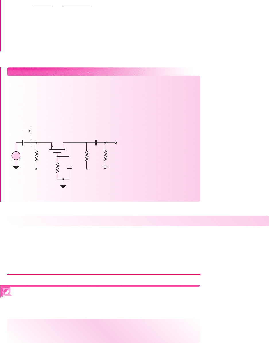
In many cases, the signal input to a common-gate circuit is a current. Figure 4.34
shows the small-signal equivalent common-gate circuit with a Norton equivalent
circuit as the signal source. We can calculate a current gain. The output current I
o
can
be written
I
o
=
R
D
R
D
+ R
L
(−g
m
V
gs
)
(4.42)
At the input we have
I
i
+ g
m
V
gs
+
V
gs
R
Si
= 0
(4.43)
or
V
gs
=−I
i
R
Si
1 + g
m
R
Si
(4.44)
The small-signal current gain is then
A
i
=
I
o
I
i
=
R
D
R
D
+ R
L
·
g
m
R
Si
1 + g
m
R
Si
(4.45)
We may note that if
R
D
R
L
and
g
m
R
Si
1
, then the current gain is essentially
unity.
I
i
R
Si
V
gs
+
–
R
D
I
o
R
L
g
m
V
gs
Flgure 4.34 Small-signal equivalent circuit of common-gate amplifier with a Norton
equivalent signal source
nea80644_ch04_205-284.qxd 06/12/2009 08:00 PM Page 235 F506 Tempwork:Dont' Del Rakesh:June:Rakesh 06-12-09:MHDQ134-04:

236 Part 1 Semiconductor Devices and Basic Applications
Input and Output Impedance
In contrast to the common-source and source-follower amplifiers, the common-gate
circuit has a low input resistance because of the transistor. However, if the input
signal is a current, a low input resistance is an advantage. The input resistance is
defined, using Figure 4.33, as
R
i
=
−V
gs
I
i
(4.46)
Since
I
i
=−g
m
V
gs
, the input resistance is
R
i
=
1
g
m
(4.47)
This result has been obtained previously.
We can find the output resistance by setting the input signal voltage equal to
zero. From Figure 4.33, we see that
V
gs
=−g
m
V
gs
R
Si
, which means that
V
gs
= 0
.
Consequently,
g
m
V
gs
= 0
. The output resistance, looking back from the load resis-
tance, is therefore
R
o
= R
D
(4.48)
4.5.2
EXAMPLE 4.10
Objective: For the common-gate circuit, determine the output voltage for a given
input current.
For the circuits shown in Figures 4.32 and 4.34, the circuit parameters are:
I
Q
= 1
mA,
V
+
= 5V
,
V
−
=−5
V,
R
G
= 100
k,
R
D
= 4
k, and
R
L
= 10
k.
The transistor parameters are:
V
TN
= 1
V,
K
n
= 1
mA/V
2
, and
λ = 0
. Assume the
input current in Figure 4.34 is
100 sin ωt μ
A and assume
R
Si
= 50
k.
Solution: The quiescent gate-to-source voltage is determined from
I
Q
= I
DQ
= K
n
(V
GSQ
− V
TN
)
2
or
1 = 1(V
GSQ
−1)
2
which yields
V
GSQ
= 2V
The small-signal transconductance is
g
m
= 2K
n
(V
GSQ
− V
TN
) = 2(1)(2 −1) = 2mA/V
From Equation (4.45), we can write the output current as
I
o
= I
i
R
D
R
D
+ R
L
·
g
m
R
Si
1 + g
m
R
Si
The output voltage is
V
o
= I
o
R
L
, so we find
V
o
= I
i
R
L
R
D
R
D
+ R
L
·
g
m
R
Si
1 + g
m
R
Si
nea80644_ch04_205-284.qxd 06/12/2009 08:00 PM Page 236 F506 Tempwork:Dont' Del Rakesh:June:Rakesh 06-12-09:MHDQ134-04:
Chapter 4 Basic FET Amplifiers 237
=
(10)(4)
4 + 10
·
(2)(50)
1 + (2)(50)
· (0.1) sin ωt
or
V
o
= 0.283 sin ωt V
Comment: The MOSFET common-gate amplifier is useful if the input signal is a
current.
EXERCISE PROBLEM
Ex 4.10: Consider the circuit shown in Figure 4.35 with circuit parameters
V
+
= 5
V,
V
−
=−5
V,
R
S
= 4
k,
R
D
= 2
k,
R
L
= 4
k and
R
G
= 50
k.
The transistor parameters are:
K
p
= 1
mA/V
2
,
V
TP
=−0.8
V, and
λ = 0
. Draw
the small-signal equivalent circuit, determine the small-signal voltage gain
A
v
=
V
o
/V
i
, and find the input resistance R
i
. (Ans.
A
v
= 2.41
,
R
i
= 0.485
k)
C
C1
R
L
R
D
R
G
v
i
v
o
R
S
C
G
C
C 2
V
+
V
–
R
i
+
–
Flgure 4.35 Figure for Exercise Ex 4.10
Test Your Understanding
TYU 4.10 For the circuit shown in Figure 4.32, the circuit parameters are:
V
+
= 5
V,
V
−
=−5
V,
R
G
= 100
k,
R
L
= 4
k, and
I
Q
= 0.5
mA. The transistor parame-
ters are
V
TN
= 1
V and
λ = 0
. The circuit is driven by a signal current source I
i
.
Redesign R
D
and g
m
such that the transfer function
V
o
/I
i
is 2.4 k and the input
resistance is
R
i
= 350
. Determine V
GSQ
and show that the transistor is biased in
the saturation region. (Ans.
g
m
= 2.86
mA/V,
R
D
= 6
k,
V
GSQ
= 1.35
V)
4.6 THE THREE BASIC
AMPLIFIER CONFIGURATIONS:
SUMMARY AND COMPARISON
Objective: • Compare the general characteristics of the three basic
amplifier configurations.
nea80644_ch04_205-284.qxd 06/12/2009 08:00 PM Page 237 F506 Tempwork:Dont' Del Rakesh:June:Rakesh 06-12-09:MHDQ134-04: