Neamen D. Microelectronics: Circuit Analysis and Design
Подождите немного. Документ загружается.

408 Part 1 Semiconductor Devices and Basic Applications
output signal. We will assume that the output resistance of the microphone is 0.5 k
as shown.
Choices: The transistor used in the design has nominal values of
β = 100
and
V
BE
(on) = 0.7
V, but the current gain for this type of transistor is assumed to be in
the range
75 ≤ β ≤ 125
because of tolerance effects. We will assume that
V
A
=∞
.
Standard resistor values are to be used in the final design, but we will assume, in this
example, that the actual resistor values are available (no tolerance effects).
Solution (Initial Design Approach): The magnitude of the voltage gain of the am-
plifier needs to be
|A
v
|=
0.4V
12 mV
= 33.3
From Equation (6.59), the approximate voltage gain of the amplifier is
|A
v
|
∼
=
R
C
R
E1
Noting from the last example that this value of gain produces an optimistically high
value, we can set
R
C
/R
E1
= 40
or
R
C
= 40 R
E1
.
The dc base-emitter loop equation is
5 = I
B
R
B
+ V
BE
(on) + I
E
(R
E1
+ R
E2
)
Assuming
β = 100
and
V
BE
(on) = 0.7
V, we can design the circuit to produce a
quiescent emitter current of, for example, 0.20 mA. We then have
5 =
(0.20)
(101)
(100) + 0.70 +(0.20)(R
E1
+ R
E2
)
which yields
R
E1
+ R
E2
= 20.5k
Assuming
I
E
∼
=
I
C
and designing the circuit such that
V
CEQ
= 4
V, the collector–
emitter loop equation produces
5 + 5 = I
C
R
C
+ V
CEQ
+ I
E
(R
E1
+ R
E2
) = (0.2)R
C
+4 +(0.2)(20.5)
or
R
C
= 9.5k
Then
R
E1
=
R
C
40
=
9.5
40
= 0.238 k
and
R
E2
= 20.3k
.
Trade-offs: From Appendix C, we will pick standard resistor values of
R
E1
= 240
,
R
E2
= 20 k
, and
R
C
= 10 k
. We will assume that these resistor
values are available and will investigate the effects of the variation in transistor cur-
rent gain
β
.
The various parameters of the circuit for three values of
β
are shown in the fol-
lowing table. The output voltage
V
o
is the result of a 12 mV input signal.
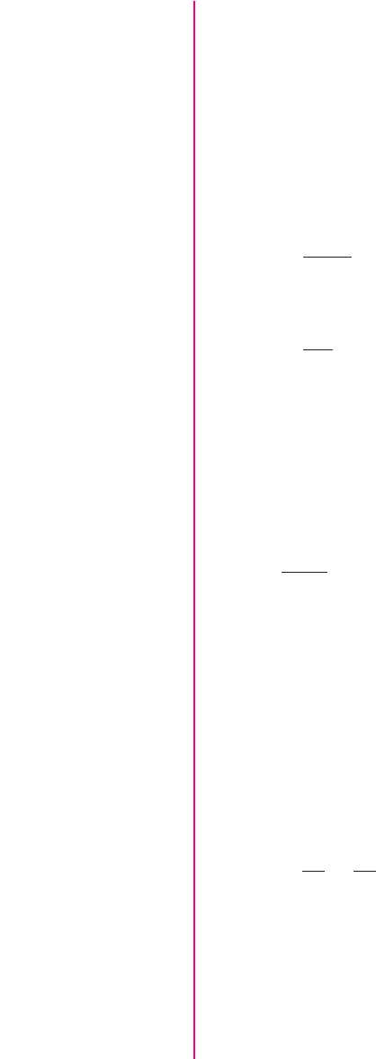
nea80644_ch06_369-468.qxd 06/13/2009 07:32 PM Page 408 F506 Hard disk:Desktop Folder:Rakesh:MHDQ134-06:
Chapter 6 Basic BJT Amplifiers 409
12 mV
– 5 V
5 V
V
+
+
–
100 kΩ
10 kΩ
2N3904
240 Ω
20 kΩ
100 m F
V
–
00
0
0
0
+
–
100 mF
C
1
C
5
Q
1
R
B
R
E1
R
E2
R
C
v
3
v
out
+
–
Figure 6.37 PSpice circuit schematic diagram for Example 6.7
One important point to note is that, the output voltage is less than the design ob-
jective of 0.4 V for a 12 mV input signal. This effect will be discussed further in the
next section involving the computer simulation.
A second point to note is that the quiescent collector current, small-signal volt-
age gain, and output voltage are relatively insensitive to the current gain
β
. This sta-
bility is a direct result of including the emitter resistor
R
E1
.
Computer Simulation: Since we used approximation techniques in our design, we can
use PSpice to give us a more accurate valuation of the circuit for the standard resistor
values that were chosen. Figure 6.37 shows the PSpice circuit schematic diagram.
β I
CQ
(mA) r
π
(k) |A
v
| V
o
(V)
75 0.197 9.90 26.1 0.313
100 0.201 12.9 26.4 0.317
125 0.203 16.0 26.6 0.319
Using the standard resistor values and the 2N3904 transistor, the output signal
voltage produced by a 12 mV input signal is 323 mV. A frequency of 2 kHz and ca-
pacitor values of 100
μ
F were used in the simulation. The magnitude of the output
signal is slightly less than the desired value of 400 mV. The principal reason for the
difference is that the
r
π
parameter of the transistor was neglected in the design. For a
collector current of approximately
I
C
= 0.2
mA,
r
π
can be significant.
In order to increase the small-signal voltage gain, a smaller value of
R
E1
is nec-
essary. For
R
E1
= 160
, the output signal voltage is 410 mV, which is very close to
the desired value.
Design Pointer: Approximation techniques are extremely useful in an initial elec-
tronic circuit design. A computer simulation, such as PSpice, can then be used to ver-
ify the design. Slight changes in the design can then be made to meet the required
specifications.
nea80644_ch06_369-468.qxd 06/13/2009 07:32 PM Page 409 F506 Hard disk:Desktop Folder:Rakesh:MHDQ134-06:
410 Part 1 Semiconductor Devices and Basic Applications
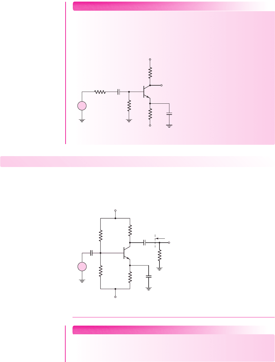
Test Your Understanding
TYU 6.7 For the circuit in Figure 6.39, let
β = 125
,
V
BE
(on) = 0.7
V, and
V
A
=
200 V. (a) Determine the small-signal voltage gain
A
v
. (b) Determine the output
resistance
R
o
. (Ans. (a)
A
v
=−50.5
(b)
R
o
= 2.28 k
)
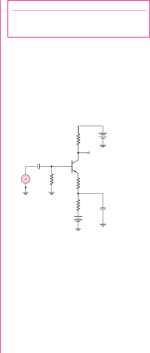
V
+
V
–
v
s
v
O
C
C
C
E
R
B
R
E
R
S
R
C
+
–
Figure 6.38 Figure for Exercise Ex 6.7
R
2
= 20 kΩ
R
1
= 20 kΩ
R
C
= 2.3 kΩ
R
E
=
5 kΩ
v
s
+5 V
–5 V
C
C1
C
C2
v
o
C
E
R
L
=
5 kΩ
R
o
+
–
Figure 6.39 Figure for Exercise TYU 6.7
COMPUTER ANALYSIS EXERCISE
PS 6.3: (a) Using a PSpice simulation, determine the voltage gain of the circuit
shown in Figure 6.39. (b) Repeat Part (a) if
R
L
= 50 k
. What can be said about
loading effects?
EXERCISE PROBLEM
Ex 6.7: The circuit in Figure 6.38 has parameters
V
+
= 5
V,
V
−
=−5
V,
R
E
= 4
k
,
R
C
= 4
k
,
R
B
= 100
k
, and
R
S
= 0.5
k
. The transistor parame-
ters are
β = 120
,
V
BE
(on) = 0.7
V, and
V
A
= 80
V. (a) Determine the input
resistance seen by the signal source. (b) Find the small-signal voltage gain.
(Ans. (a)
R
i
= 3.91
k
, (b)
A
v
=−114)
nea80644_ch06_369-468.qxd 06/13/2009 07:32 PM Page 410 F506 Hard disk:Desktop Folder:Rakesh:MHDQ134-06:
Chapter 6 Basic BJT Amplifiers 411
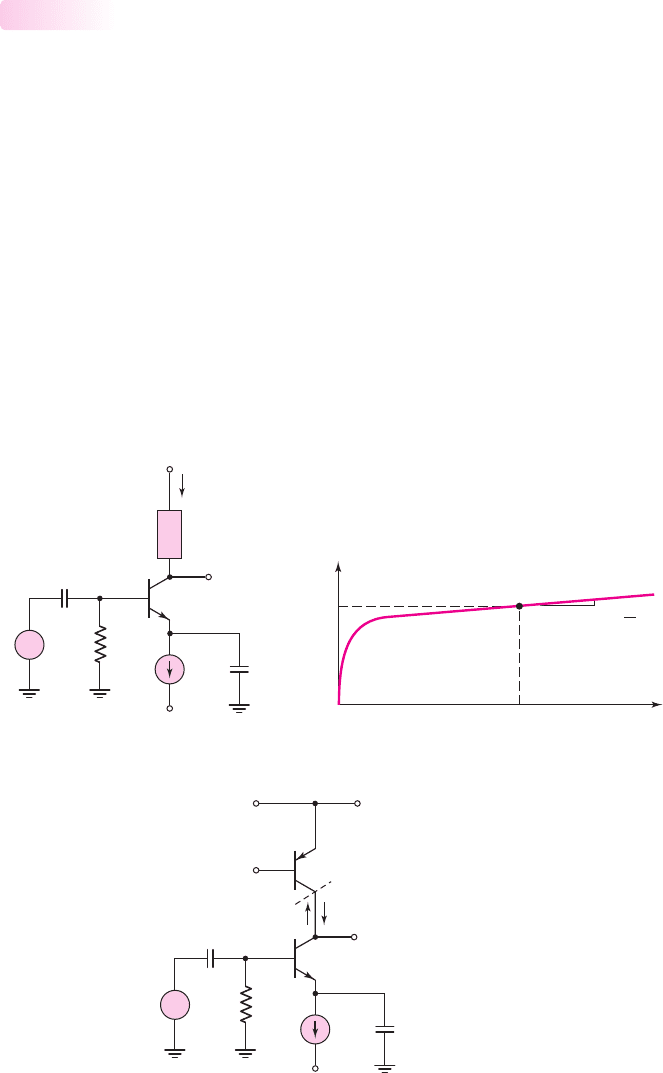
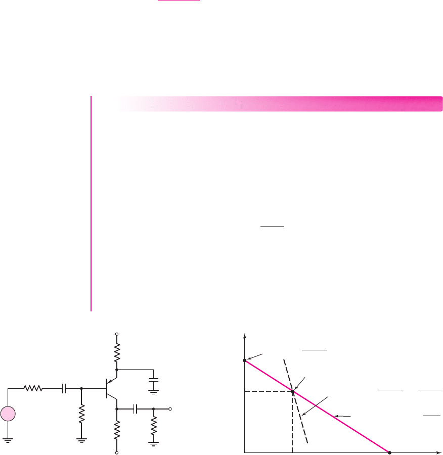
Advanced Common-Emitter Amplifier Concepts
Our previous analysis of common-emitter circuits assumed constant load or collector
resistances. The common-emitter circuit shown in Figure 6.40(a) is biased with a
constant-current source and contains a nonlinear, rather than a constant, collector
resistor. Assume the current–voltage characteristics of the nonlinear resistor are
described by the curve in Figure 6.40(b). The curve in Figure 6.40(b) can be gener-
ated using the pnp transistor as shown in Figure 6.40(c). The transistor is biased at a
constant
V
EB
voltage. This transistor is now the load device and, since transistors are
active devices, this load is referred to as an active load. We will encounter active
loads in much more detail in Part 2 of the text.
Neglecting the base current in Figure 6.40(a), we can assume the quiescent
current and voltage values of the load device are
I
Q
= I
CQ
and
V
RQ
as shown in Fig-
ure 6.40(b). At the Q-point of the load device, assume the incremental resistance
v
R
/i
C
is
r
c
.
6.4.4
i
C
I
CQ
v
R
V
RQ
Slope =
1
r
c
V
+
V
–
v
s
v
O
Q
o
C
C
C
E
I
Q
R
B
R
C
+
–
v
R
i
C
+
–
(a) (b)
V
+
+
+
–
–
i
C
r
c
V
–
v
s
v
O
v
EC
= v
R
V
EB
Q
o
C
C
C
E
I
Q
R
B
+
–
(c)
Figure 6.40 (a) A common-emitter circuit with current source biasing and a nonlinear load
resistor, (b) current–voltage characteristics of the nonlinear load resistor, and (c) pnp
transistor that can be used to generate the nonlinear load characteristics
nea80644_ch06_369-468.qxd 06/13/2009 07:32 PM Page 411 F506 Hard disk:Desktop Folder:Rakesh:MHDQ134-06:

412 Part 1 Semiconductor Devices and Basic Applications
EXAMPLE 6.8
Objective: Determine the small-signal voltage gain of a common-emitter circuit
with a nonlinear load resistance.
Assume the circuit shown in Figure 6.40(a) is biased at
I
Q
= 0.5
mA, and the
transistor parameters are
β = 120
and
V
A
= 80
V. Also assume that nonlinear small-
signal collector resistance is
r
c
= 120 k
.
Solution: For a transistor current gain of
β = 120
,
I
CQ
∼
=
I
EQ
= I
Q
, and the small-
signal hybrid-π parameters are
g
m
=
I
CQ
V
T
=
0.5
0.026
= 19.2mA/V
and
r
o
=
V
A
I
CQ
=
80
0.5
= 160 k
The small-signal voltage gain is therefore
A
v
=−g
m
(r
o
r
c
) =−(19.2)(160120) =−1317
Comment: As we will see further in Part 2 of this text, the nonlinear resistor
r
c
is
produced by the I–V characteristics of another bipolar transistor. Because the result-
ing effective load resistance is large, a very large small-signal voltage gain is pro-
duced. A large effective load resistance
r
c
means that the output resistance
r
o
of the
amplifying transistor cannot be neglected; therefore, the loading effects must be
taken into account.
EXERCISE PROBLEM
Ex 6.8: (a) Assume the circuit shown in Figure 6.40(a) is biased at
I
Q
= 0.25
mA
and assume transistor parameters
β = 100
and
V
A
= 100
V. Assume the small-
signal nonlinear collector resistance is
r
c
= 100 k
. Determine the small-signal
voltage gain. (b) Repeat part (a) assuming that a small-signal load resistance
of
r
L
= 100 k
is connected between the output terminal and ground. (Ans.
(a)
A
v
=−769
; (b)
A
v
=−427
)
R
B
r
p
V
p
r
c
r
o
V
o
g
m
V
p
V
s
+
–
+
–
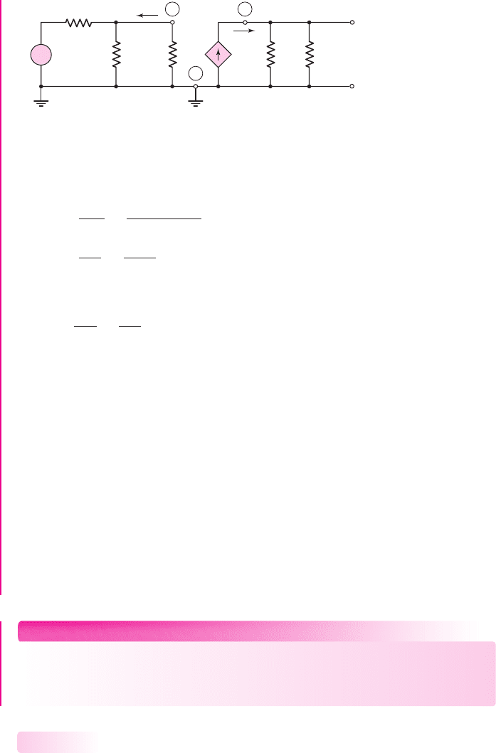
Figure 6.41 Small-signal equivalent circuit of the circuit in Figure 6.40(a)
The small-signal equivalent circuit of the common-emitter amplifier circuit in
Figure 6.40(a) is shown in Figure 6.41. The collector resistor
R
C
is replaced by the
small-signal equivalent resistance
r
c
that exists at the Q-point. The small-signal volt-
age gain is then, assuming an ideal voltage signal source,
A
v
=
V
o
V
s
=−g
m
(r
o
r
c
)
(6.60)
nea80644_ch06_369-468.qxd 06/13/2009 07:32 PM Page 412 F506 Hard disk:Desktop Folder:Rakesh:MHDQ134-06:
Chapter 6 Basic BJT Amplifiers 413
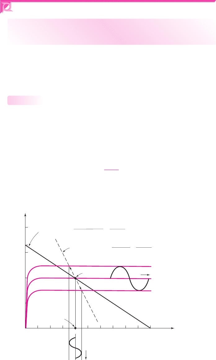
6.5 AC LOAD LINE ANALYSIS
Objective: • Understand the concept of the ac load line and calculate
the maximum symmetrical swing of the output signal.
A dc load line gives us a way of visualizing the relationship between the Q-point and
the transistor characteristics. When capacitors are included in a transistor circuit, a
new effective load line, called an ac load line, may exist. The ac load line helps in
visualizing the relationship between the small-signal response and the transistor
characteristics. The ac operating region is on the ac load line.
AC Load Line
The circuit in Figure 6.36 has emitter resistors and an emitter bypass capacitor. The
dc load line is found by writing a Kirchhoff voltage law (KVL) equation around the
collector–emitter loop, as follows:
V
+
= I
C
R
C
+ V
CE
+ I
E
(R
E1
+ R
E2
) + V
−
(6.61)
Noting that
I
E
= [(1 +β)/β]I
C
, Equation (6.61) can be written as
V
CE
= (V
+
− V
−
) − I
C
R
C
+
1 + β
β
(R
E1
+ R
E2
)
(6.62)
which is the equation of the dc load line. For the parameters and standard resistor val-
ues found in Example 6.7, the dc load line and the Q-point are plotted in Figure 6.42.
If
β 1
, then we can approximate
(1 + β)/β
∼
=
1
.
6.5.1
0.40
0.30
0.33
0.20
0.10
i
C
(mA)
i
B
I
BQ
= 2 mA
V
CEQ
= 4 V
v
CE
(V)
0246810
DC load line, slope ≅ =
–1
R
C
+ R
E1
+ R
E2
–1
30.2 kΩ
AC load line, slope =
Q-point
Time
Time
=
–1
R
C
+ R
E1
–1
10.2 kΩ
Figure 6.42 The dc and ac load lines for the circuit in Figure 6.36, and the signal responses
to input signal
nea80644_ch06_369-468.qxd 06/13/2009 07:32 PM Page 413 F506 Hard disk:Desktop Folder:Rakesh:MHDQ134-06:
414 Part 1 Semiconductor Devices and Basic Applications
i
C
(mA)
v
EC
(V)
6.53
0.894
= 1.33 mA
V
+
– V
–
V
+
– V
–
= 20 V
R
C
+ R
E
I
C
(max) ≈
Q-point
dc load line, slope ≈ –
=–
1
1
R
C
⎜⎜
R
L
1.43 kΩ
1
15 kΩ
ac load line, slope = –
Figure 6.44 Plots of dc and ac load lines for Example 6.9
V
–
= –10 V
V
+
= +10 V
+
–
v
s
C
C1
C
C2
v
o
C
E
R
B
=
50 kΩ
R
S
= 1 kΩ
R
C
=
5 kΩ
V
EB
R
L
= 2 kΩ
R
E
= 10 kΩ
+
–
Figure 6.43 Circuit for Example 6.9
From the small-signal analysis in Example 6.7, the KVL equation around the
collector–emitter loop is
i
c
R
C
+v
ce
+i
e
R
E1
= 0
(6.63(a))
or, assuming
i
c
∼
=
i
e
, then
v
ce
=−i
c
(R
C
+ R
E1
)
(6.63(b))
This equation is the ac load line. The slope is given by
Slope =
−1
R
C
+ R
E1
The ac load line is shown in Figure 6.42. When
v
ce
= i
c
= 0
, we are at the Q-point.
When ac signals are present, we deviate about the Q-point on the ac load line.
The slope of the ac load line differs from that of the dc load line because the emitter
resistor
R
E2
is not included in the small-signal equivalent circuit. The small-signal C–E
voltage and collector current response are functions of the resistor
R
C
and
R
E1
only.
EXAMPLE 6.9
Objective: Determine the dc and ac load lines for the circuit shown in Figure 6.43.
Assume the transistor parameters are:
V
EB
(on) = 0.7
V,
β = 150
, and
V
A
=∞
.
DC Solution: The dc load line is found by writing a KVL equation around the C–E
loop, as follows:
V
+
= I
E
R
E
+ V
EC
+ I
C
R
C
+ V
−
The dc load line equation is then
V
EC
= (V
+
− V
−
) − I
C
R
C
+
1 + β
β
R
E
Assuming that
(1 + β)/β
∼
=
1
, the dc load line is plotted in Figure 6.44.
The
Q
-point values are found to be
I
BQ
= 5.96 μ
A,
I
CQ
= 0.894
mA,
I
EQ
= 0.90
mA, and
V
ECQ
= 6.53
V. The
Q
-point is also plotted in Figure 6.44.
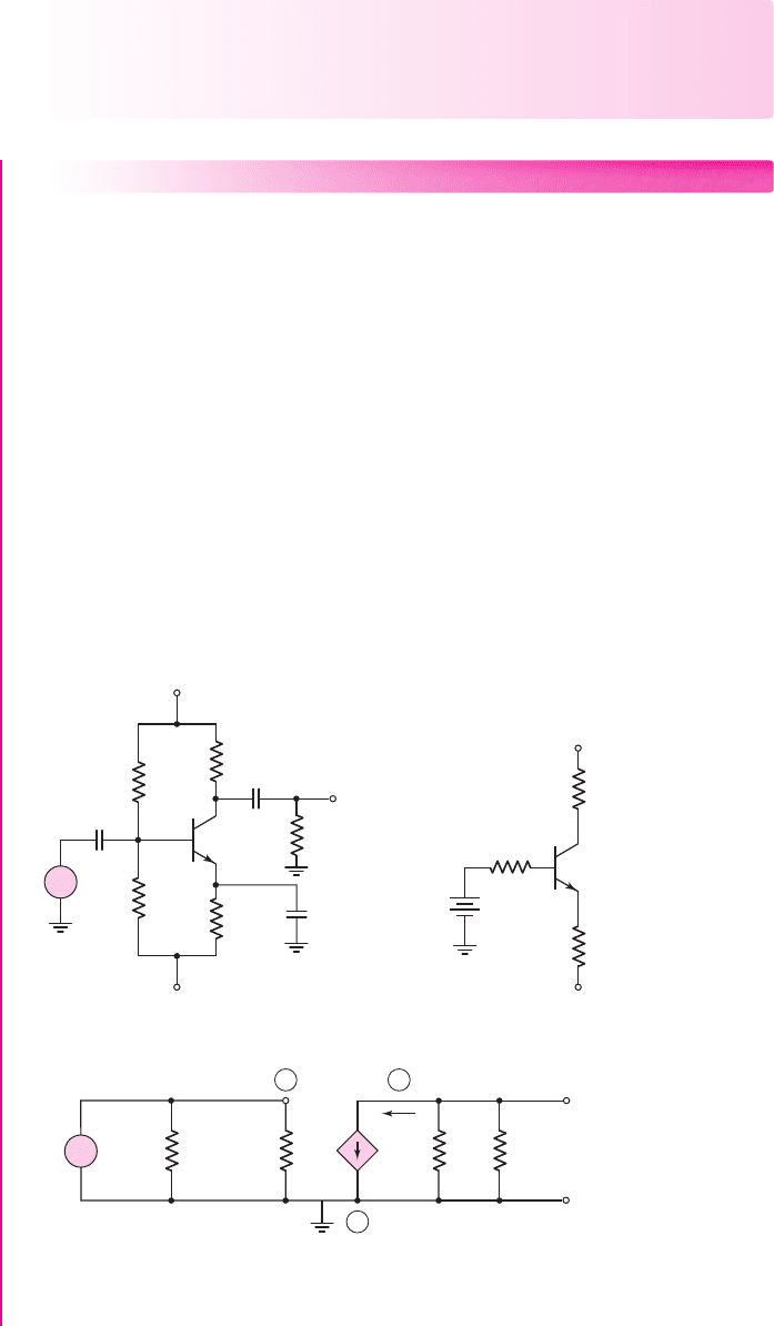
AC Solution: Assuming that all capacitors act as short circuits, the small-signal
equivalent circuit is shown in Figure 6.45. Note that the current directions and
nea80644_ch06_369-468.qxd 06/13/2009 07:32 PM Page 414 F506 Hard disk:Desktop Folder:Rakesh:MHDQ134-06:
Chapter 6 Basic BJT Amplifiers 415
voltage polarities in the hybrid-
π
equivalent circuit of the pnp transistor are reversed
compared to those of the npn device. The small-signal hybrid-
π
parameters are
r
π
=
V
T
β
I
CQ
=
(0.026)(150)
0.894
= 4.36 k
g
m
=
I
CQ
V
T
=
0.894
0.026
= 34.4 mA/V
and
r
o
=
V
A
I
CQ
=
∞
I
CQ
=∞
The small-signal output voltage, or C–E voltage, is
v
o
= v
ce
=+(g
m
v
π
)(R
C
R
L
)
where
g
m
v
π
= i
c
The ac load line, written in terms of the E–C voltage, is defined by
v
ec
=−i
c
(R
C
R
L
)
The ac load line is also plotted in Figure 6.44.
Comment: In the small-signal equivalent circuit, the large 10 k
emitter resistor is
effectively shorted by the bypass capacitor
C
E
, the load resistor
R
L
is in parallel with
R
C
as a result of the coupling capacitor
C
C2
, so that the slope of the ac load line is
substantially different than that of the dc load line.
EXERCISE PROBLEM
Ex 6.9: For the circuit in Figure 6.39, let
β = 125
,
V
BE
(on) = 0.7
V, and
V
A
= 200
V. Plot the dc and ac load lines on the same graph. (Ans.
I
CQ
=
0.840 mA, dc load line,
V
CE
= 10 − I
C
(7.3)
; ac load line,
V
ce
=−I
c
(1.58)
)
Maximum Symmetrical Swing
When symmetrical sinusoidal signals are applied to the input of an amplifier, sym-
metrical sinusoidal signals are generated at the output, as long as the amplifier oper-
ation remains linear. We can use the ac load line to determine the maximum output
symmetrical swing. If the output exceeds this limit, a portion of the output signal
will be clipped and signal distortion will occur.
6.5.2
R
B
=
50 kΩ
R
S
= 1 kΩ
R
C
=
5 kΩ
R
L
=
2 kΩ
r
p
v
p
g
m
v
p
v
s
v
o
+
–
E
BC
i
c
i
b
+
–
v
ce
+
–
Figure 6.45 The small-signal equivalent circuit for Example 6.9
nea80644_ch06_369-468.qxd 06/13/2009 07:32 PM Page 415 F506 Hard disk:Desktop Folder:Rakesh:MHDQ134-06:

416 Part 1 Semiconductor Devices and Basic Applications
EXAMPLE 6.10
Objective: Determine the maximum symmetrical swing in the output voltage of the
circuit given in Figure 6.43.
Solution: The ac load line is given in Figure 6.44. The maximum negative swing in
the collector current is from 0.894 mA to zero; therefore, the maximum possible
symmetrical peak-to-peak ac collector current is
i
c
= 2(0.894) = 1.79 mA
The maximum symmetrical peak-to-peak output voltage is given by
|v
ec
|=|i
c
|(R
C
R
L
) = (1.79)(52) = 2.56 V
Therefore, the maximum instantaneous collector current is
i
C
= I
CQ
+
1
2
|i
c
|=0.894 + 0.894 = 1.79 mA
Comment: Considering the Q-point and the maximum swing in the C–E voltage, the
transistor remains biased in the forward-active region. Note that the maximum in-
stantaneous collector current, 1.79 mA, is larger than the maximum dc collector cur-
rent, 1.33 mA, as determined from the dc load line. This apparent anomaly is due to
the different resistance in the C–E circuit for the ac signal and the dc signal.
EXERCISE PROBLEM
Ex 6.10: Reconsider the circuit in Figure 6.38. Let
β = 120
,
V
BE
(on) = 0.7
V, and
V
A
=∞
. The circuit parameters are given in Exercise Ex 6.7. (a) Plot the dc and ac
load lines on the same graph. (b) Determine the Q-point values. (c) Determine the
maximum symmetrical swing in the output voltage for
i
C
> 0
and
0.5 ≤ v
CE
≤ 9
V. (Ans. (b)
I
CQ
= 0.884
mA,
V
CEQ
= 2.9
V; (c)
v
ce
= 4.8
V,
peak-to-peak)
Note: In considering Figure 6.42, it appears that the ac output signal is
smaller for the ac load line compared to the dc load line. This is true for a given
sinusoidal input base current. However, the required input signal voltage
v
s
is
substantially smaller for the ac load line to generate the given ac base current.
This means the voltage gain for the ac load line is larger than that for the dc load
line.
Problem-Solving Technique: Maximum Symmetrical Swing
Again, since we are dealing with linear amplifier circuits, superposition applies so
that we can add the dc and ac analysis results. To design a BJT amplifier for max-
imum symmetrical swing, we perform the following steps.
1. Write the dc load line equation that relates the quiescent values
I
CQ
and
V
CEQ
.
2. Write the ac load line equation that relates the ac values
i
c
and
v
ce
: v
ce
=
−i
c
R
eq
where
R
eq
is the effective ac resistance in the collector–emitter circuit.
3. In general, we can write
i
c
= I
CQ
− I
C
(min)
, where
I
C
(min)
is zero or some
other specified minimum collector current.
nea80644_ch06_369-468.qxd 06/13/2009 07:32 PM Page 416 F506 Hard disk:Desktop Folder:Rakesh:MHDQ134-06:
Chapter 6 Basic BJT Amplifiers 417
4. In general, we can write
v
ce
= V
CEQ
− V
CE
(min)
, where
V
CE
(min)
is some
specified minimum collector-emitter voltage.
5. The above four equations can be combined to yield the optimum
I
CQ
and
V
CEQ
values to obtain the maximum symmetrical swing in the output signal.
DESIGN EXAMPLE 6.11
Objective: Design a circuit to achieve a maximum symmetrical swing in the output
voltage.
Specifications: The circuit configuration to be designed is shown in Figure 6.46a.
The circuit is to be designed to be bias stable. The minimum collector current is
to be
I
C
(min) = 0.1
mA and the minimum collector-emitter voltage is to be
V
CE
(min) = 1
V.
Choices: Assume nominal resistance values of
R
E
= 2k
and
R
C
= 7k
. Let
R
TH
= R
1
R
2
= (0.1)(1 +β)R
E
= 24.2k
. Assume transistor parameters of
β = 120
,
V
BE
(on) = 0.7
V, and
V
A
=∞
.
Solution (Q-Point): The dc equivalent circuit is shown in Figure 6.46(b) and the
midband small-signal equivalent circuit is shown in Figure 6.46(c).
The dc load line, from Figure 6.46(b), is (assuming
I
C
∼
=
I
E
)
V
CE
= 10 − I
C
(R
C
+ R
E
) = 10 − I
C
(9)
R
C
R
L
r
p
V
p
g
m
V
p
V
s
V
o
–
+
E
B C
I
c
+
–
V
ce
+
–
(c)
(a) (b)
+5 V
–5 V
v
s
C
C1
C
C2
v
o
R
2
R
1
R
E
=
2 kΩ
R
L
=
10 kΩ
R
C
= 7 kΩ
C
E
+
–
+5 V
–5 V
R
C
R
E
R
TH
V
TH
+
–
R
1
⎜⎜ R
2
Figure 6.46 (a) Circuit for Example 6.11, (b) Thevenin equivalent circuit, and (c) small-
signal equivalent circuit
nea80644_ch06_369-468.qxd 06/13/2009 07:32 PM Page 417 F506 Hard disk:Desktop Folder:Rakesh:MHDQ134-06: