Neamen D. Microelectronics: Circuit Analysis and Design
Подождите немного. Документ загружается.

438 Part 1 Semiconductor Devices and Basic Applications
The dc and ac analyses of a multitransistor circuit become more complex com-
pared to those for a single-transistor circuit. In this situation, a computer simulation
of the circuit, without a hand analysis, is extremely useful.
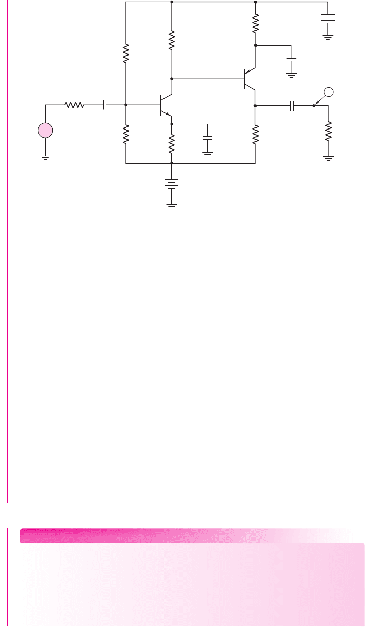
The PSpice circuit schematic is shown in Figure 6.68. The resulting
Q
-point values
are
I
CQ1
= 2.54
mA,
I
CQ2
= 1.18
mA,
V
ECQ1
= 1.10
V, and
V
CEQ2
= 1.79
V. The ac
common-emitter current gains are
β
1
= 173
and
β
2
= 157
.
A
1 μV
sinusoidal signal is applied. The sinusoidal voltage at the collector of
Q
2
is
51 μV
and the sinusoidal voltage at the output is 4.79 mV. The overall voltage gain
is then 4790. We will show, in later chapters, that even larger voltage gains can be ob-
tained by replacing the discrete collector resistors with active loads.
Comment: We can see from the Q-point values that the collector–emitter voltage
of each transistor is quite small. This implies that the maximum symmetrical swing
in the output voltage is limited to a fairly small value. These Q-point values can be
increased by a slight redesign of the circuit.
Discussion: The transistors used in this PSpice analysis of the circuit were standard
bipolar transistors from the PSpice library. We must keep in mind that, for the com-
puter simulation to be valid, the models of the devices used in the simulation must
match those of the actual devices used in the circuit. If the actual transistor charac-
teristics were substantially different from those used in the computer simulation, then
the results of the computer analysis would not be accurate.
EXERCISE PROBLEM
Ex 6.15: For each transistor in the circuit in Figure 6.69, the parameters are:
β = 125
,
V
BE
(on) = 0.7
V, and
r
o
=∞
. (a) Determine the Q-points of each tran-
sistor. (b) Find the overall small-signal voltage gain
A
v
= V
o
/V
s
. (c) Determine
the input resistance R
i
and the output resistance R
o
. (Ans. (a)
I
CQ1
= 0.364
mA,
V
CEQ1
= 7.92
V,
I
CQ2
= 4.82
mA,
V
CEQ2
= 2.71
V (b)
A
v
=−17.7
(c)
R
i
=
4.76 k
,
R
o
= 43.7
)
0
0
0
0
0
0
–5 V
+
–
0.5 kΩ
50 kΩ
1.5 kΩ
2 kΩ
5 kΩ
100 kΩ
5 kΩ
2N3904
2N3906
2 kΩ
1 mV
100 mF
100 mF
100 mF
100 mF
V
3
V
2
R
2
R
1
Q
2
Q
1
C
C1
R
E1
R
C1
R
C2
C
C2
R
E2
C
E2
R
L
C
E1
R
S
V
5 V
+
–
V
1
+
–
~
Figure 6.68 PSpice circuit schematic for Example 6.15
nea80644_ch06_369-468.qxd 06/13/2009 07:32 PM Page 438 F506 Hard disk:Desktop Folder:Rakesh:MHDQ134-06:
Chapter 6 Basic BJT Amplifiers 439
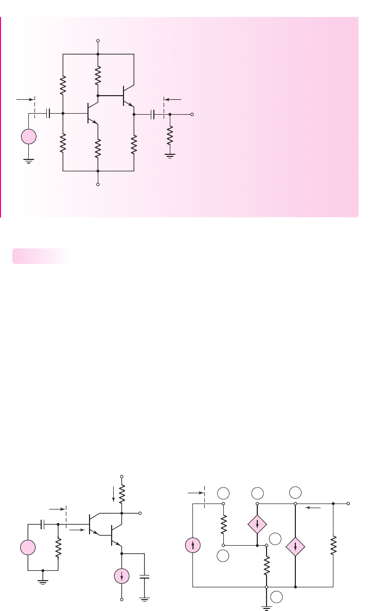
Multistage Circuit: Darlington Pair Configuration
In some applications, it would be desirable to have a bipolar transistor with a much
larger current gain than can normally be obtained. Figure 6.70(a) shows a multitran-
sistor configuration, called a Darlington pair or a Darlington configuration, that
provides increased current gain.
The small-signal equivalent in which the input signal is assumed to be a current
source, is shown in Figure 6.70(b). We will use the input current source to determine
the current gain of the circuit. To determine the small-signal current gain
A
i
= I
o
/I
i
,
we see that
V
π1
= I
i
r
π1
(6.103)
Therefore,
g
m1
V
π1
= g
m1
r
π1
I
i
= β
1
I
i
(6.104)
6.9.2
R
2
=
6 kΩ
R
1
=
70 kΩ
R
C1
=
5 kΩ
R
E1
=
0.2 kΩ
v
s
C
C1
C
C2
+
–
V
+
= +5 V
V
–
= –5 V
v
o
R
o
R
E2
=
1.5 kΩ
R
L
=
10 kΩ
Q
1
Q
2
R
i
+
–
Figure 6.69 Figure for Exercise Ex 6.15
R
B
v
s
v
o
C
E
I
Eo
C
C
+
–
R
i
R
C
i
i
i
c
Q
1
V
–
V
+
Q
2
+
–
+
–
+
–
V
i
r
p1
r
p 2
V
p1
V
p 2
I
i
R
i
V
o
R
C
g
m2
V
p 2
g
m1
V
p 1
I
o
B
1
E
1
C
1
B
2
E
2
C
2
(a) (b)
+
–
Figure 6.70 (a) A Darlington pair configuration; (b) small-signal equivalent circuit
nea80644_ch06_369-468.qxd 06/13/2009 07:32 PM Page 439 F506 Hard disk:Desktop Folder:Rakesh:MHDQ134-06:

440 Part 1 Semiconductor Devices and Basic Applications
Then,
V
π2
= (I
i
+β
1
I
i
)r
π2
(6.105)
The output current is
I
o
= g
m1
V
π1
+ g
m2
V
π2
= β
1
I
i
+β
2
(1 + β
1
)I
i
(6.106)
where
g
m2
r
π2
= β
2
. The overall current gain is then
A
i
=
I
o
I
i
= β
1
+β
2
(1 + β
1
)
∼
=
β
1
β
2
(6.107)
From Equation (6.107), we see that the overall small-signal current gain of the
Darlington pair is essentially the product of the individual current gains.
The input resistance is
R
i
= V
i
/I
i
. We can write that
V
i
= V
π1
+ V
π2
= I
i
r
π1
+ I
i
(1 + β
1
)r
π2
(6.108)
so that
R
i
= r
π1
+(1 +β
1
)r
π2
(6.109)
The base of transistor Q
2
is connected to the emitter of Q
1
, which means that the
input resistance to Q
2
is multiplied by the factor (
1 + β
1
), as we saw in circuits with
emitter resistors. We can write
r
π1
=
β
1
V
T
I
CQ1
(6.110)
and
I
CQ1
∼
=
1
CQ2
β
2
(6.111)
Therefore,
r
π1
= β
1
β
2
V
T
I
CQ2
= β
1
r
π2
(6.112)
From Equation (6.109), the input resistance is then approximately
R
i
∼
=
2β
1
r
π2
(6.113)
We see from these equations that the overall gain of the Darlington pair is
large. At the same time, the input resistance tends to be large, because of the
β
multiplication.
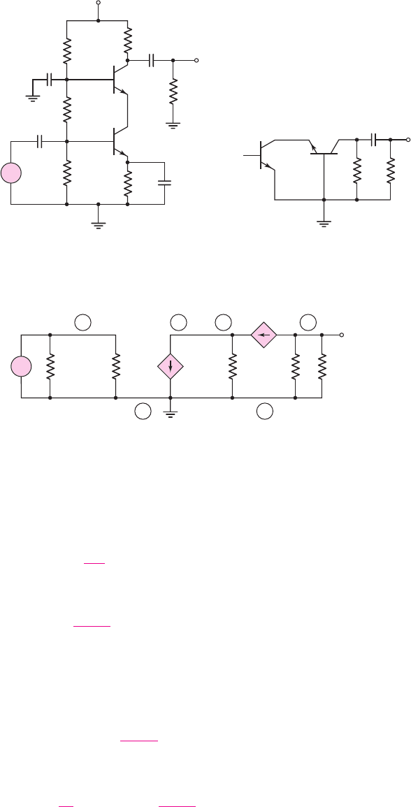
Multistage Circuit: Cascode Configuration
A slightly different multistage configuration, called a cascode configuration, is
shown in Figure 6.71(a). The input is into a common-emitter amplifier (Q
1
), which
drives a common-base amplifier (Q
2
). The ac equivalent circuit is shown in Fig-
ure 6.71(b). We see that the output signal current of Q
1
is the input signal of Q
2
. We
mentioned previously that, normally, the input signal of a common-base configura-
tion is to be a current. One advantage of this circuit is that the output resistance
looking into the collector of Q
2
is much larger than the output resistance of a simple
common-emitter circuit. Another important advantage of this circuit is in the fre-
quency response, as we will see in Chapter 7.
6.9.3
nea80644_ch06_369-468.qxd 06/13/2009 07:32 PM Page 440 F506 Hard disk:Desktop Folder:Rakesh:MHDQ134-06:
Chapter 6 Basic BJT Amplifiers 441
The small-signal equivalent circuit is shown in Figure 6.72 for the case when the
capacitors act as short circuits. We see that
V
π1
= V
s
since we are assuming an ideal
signal voltage source. Writing a KCL equation at E
2
, we have
g
m1
V
π1
=
V
π2
r
π2
+ g
m2
V
π2
(6.114)
Solving for the control voltage
V
π2
(noting that
V
π1
= V
s
), we find
V
π2
=
r
π2
1 + β
2
(g
m1
V
s
)
(6.115)
where
β
2
= g
m2
r
π2
. The output voltage is
V
o
=−(g
m2
V
π2
)(R
C
R
L
)
(6.116(a))
or
V
o
=−g
m1
g
m2
r
π2
1 + β
2
(R
C
R
L
)V
s
(6.116(b))
Therefore, the small-signal voltage gain is
A
v
=
V
o
V
s
=−g
m1
g
m2
r
π2
1 + β
2
(R
C
R
L
)
(6.117)
R
3
R
1
R
E
R
C
R
C
V
CC
C
C1
C
C2
C
E
C
B
R
2
R
L
R
L
v
o
v
o
v
s
Q
1
Q
1
Q
2
Q
2
(a) (b)
+
–
Figure 6.71 (a) Cascode amplifier and (b) the ac equivalent circuit
+
–
V
p
1
g
m1
V
p
1
V
s
r
p
1
r
p
2
R
C
R
L
V
o
g
m2
V
p
2
+
–
V
p
2
R
2
⎜⎜ R
3
B
1
C
1
E
2
C
2
E
1
B
2
+
–
Figure 6.72 Small-signal equivalent circuit of the cascode configuration
nea80644_ch06_369-468.qxd 06/13/2009 07:32 PM Page 441 F506 Hard disk:Desktop Folder:Rakesh:MHDQ134-06:

442 Part 1 Semiconductor Devices and Basic Applications
An examination of Equation (6.117) shows
g
m2
r
π2
1 + β
2
=
β
2
1 + β
2
∼
=
1
(6.118)
The gain of the cascode amplifier is then approximately
A
v
∼
=
−g
m1
(R
C
R
L
)
(6.119)
which is the same as for a single-stage common-emitter amplifier. This result is to be
expected since the current gain of the common-base circuit is essentially unity.
Test Your Understanding
TYU 6.16 Consider the circuit in Figure 6.70(a). Let
β = 100
,
V
BE
(on) = 0.7
V,
and
V
A
=∞
for each transistor. Assume
R
B
= 10 k
,
R
C
= 4k
,
I
Eo
= 1
mA,
V
+
= 5
V, and
V
−
=−5V
. (a) Determine the Q-point values for each transistor.
(b) Calculate the small-signal hybrid-
π
parameters for each transistor. (c) Find the
overall small-signal voltage gain
A
v
= V
o
/V
s
. (d) Find the input resistance R
i
.
(Ans. (a)
I
CQ1
= 0.0098
mA,
V
CEQ1
= 1.7
V,
I
CQ2
= 0.990
mA,
V
CEQ2
= 2.4
V
(b)
r
π1
= 265 k
,
g
m1
= 0.377 mA/V
,
r
π2
= 2.63 k
,
g
m2
= 38.1
mA/V (c)
A
v
=
−77.0
(d)
R
i
= 531 k
)
TYU 6.17 Consider the cascode circuit in Figure 6.71(a). Let
β = 100
,
V
BE
(on) = 0.7
V, and
V
A
=∞
for each transistor. Let
V
CC
= 9
V and
R
L
= 10
k
.
(a) Design the circuit such that
V
CE1
= V
CE2
= 2.5
V,
V
RE
= 0.7
V,
I
C1
∼
=
I
C2
∼
=
1
mA, and
I
R1
∼
=
I
R2
∼
=
I
R3
∼
=
0.1
mA. (Hint: Neglect the dc base currents.)
(b) Determine the small-signal hybrid-
π
parameters for each transistor. (c) Deter-
mine the small-signal voltage gain
A
v
= V
o
/V
s
. (Ans. (a)
R
1
= 51
k
,
R
2
= 25
k
,
R
3
= 14
k
,
R
E
= 0.7
k
,
R
C
= 3.3
k
; (b)
g
m
= 38.46
mA/V,
r
π
= 2.6
k
;
(c)
A
v
=−94.5)
6.10 POWER CONSIDERATIONS
Objective: • Analyze the ac and dc power dissipation in a transistor
amplifier and understand the concept of signal power gain.
As mentioned previously, an amplifier produces a small-signal power gain. Since
energy must be conserved, the question naturally arises as to the source of this
“extra” signal power. We will see that the “extra” signal power delivered to a load is
a result of a redistribution of power between the load and the transistor.
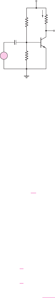
Consider the simple common-emitter circuit shown in Figure 6.73 in which
an ideal signal voltage source is connected at the input. The dc power supplied
by the V
CC
voltage source P
CC
, the dc power dissipated or supplied to the collec-
tor resistor P
RC
, and the dc power dissipated in the transistor P
Q
are given,
respectively, as
nea80644_ch06_369-468.qxd 06/13/2009 07:32 PM Page 442 F506 Hard disk:Desktop Folder:Rakesh:MHDQ134-06:
Chapter 6 Basic BJT Amplifiers 443
P
CC
= I
CQ
V
CC
+ P
Bias
(6.120(a))
P
RC
= I
2
CQ
R
C
(6.120(b))
and
P
Q
= I
CQ
V
CEQ
+ I
BQ
V
BEQ
∼
=
I
CQ
V
CEQ
(6.120(c))
The term
P
Bias
is the power dissipated in the bias resistors R
1
and R
2
. Normally in a
transistor
I
CQ
I
BQ
, so the power dissipated is primarily a function of the collector
current and collector–emitter voltage.
If the signal voltage is given by
v
s
= V
p
cos ωt
(6.121)
then the total base current is given by
i
B
= I
BQ
+
V
p
r
π
cos ωt = I
BQ
+ I
b
cos ωt
(6.122)
and the total collector current is
i
C
= I
CQ
+β I
b
cos ωt = I
CQ
+ I
c
cos ωt
(6.123)
The total instantaneous collector-emitter voltage is
v
CE
= V
CC
−i
C
R
C
= V
CC
−(I
CQ
+ I
c
cos ωt)R
C
= V
CEQ
− I
c
R
C
cos ωt
(6.124)
The average power, including ac signals, supplied by the voltage source V
CC
is
given by
¯p
cc
=
1
T
T
0
V
CC
·i
C
dt + P
Bias
=
1
T
T
0
V
CC
· [I
CQ
+ I
c
cos ωt] dt + P
Bias
= V
CC
I
CQ
+
V
CC
I
c
T
T
0
cos ωtdt+ P
Bias
(6.125)
+
–
v
s
i
C
C
C
+
–
v
CE
v
o
R
C
V
CC
R
2
R
1
Figure 6.73 Simple common-emitter amplifier for power calculations
nea80644_ch06_369-468.qxd 06/13/2009 07:32 PM Page 443 F506 Hard disk:Desktop Folder:Rakesh:MHDQ134-06:

444 Part 1 Semiconductor Devices and Basic Applications
Since the integral of the cosine function over one period is zero, the average power
supplied by the voltage source is the same as the dc power supplied. The dc voltage
source does not supply additional power.
The average power delivered to the load R
C
is found from
¯p
RC
=
1
T
T
0
i
2
C
R
C
dt =
R
C
T
T
0
[I
CQ
+ I
c
cos ωt]
2
dt
=
I
2
CQ
R
C
T
T
0
dt +
2I
CQ
I
c
T
T
0
cos ωtdt+
I
2
c
R
C
T
T
0
cos
2
ωtdt
(6.126)
The middle term of this last expression is again zero, so
¯p
RC
= I
2
CQ
R
C
+
1
2
I
2
c
R
C
(6.127)
The average power delivered to the load has increased because of the signal source.
This is expected in an amplifier.
Now, the average power dissipated in the transistor is
¯p
Q
=
1
T
T
0
i
C
· v
CE
dt
=
1
T
T
0
[I
CQ
+ I
c
cos ωt] ·[V
CEQ
− I
c
R
C
cos ωt] dt
(6.128)
which produces
¯p
Q
= I
CQ
V
CEQ
−
I
2
c
R
C
T
T
0
cos
2
ωtdt
(6.129(a))
or
¯p
Q
= I
CQ
V
CEQ
−
1
2
I
2
c
R
C
(6.129(b))
From Equation (6.129(b)), we can deduce that the average power dissipated in
the transistor decreases when an ac signal is applied. The V
CC
source still supplies all
of the power, but the input signal changes the relative distribution of power between
the transistor and the load.
Test Your Understanding
TYU 6.18 In the circuit in Figure 6.74 the transistor parameters are:
β = 80
,
V
BE
(on) = 0.7
V, and
V
A
=∞
. Determine the average power dissipated in R
C
, R
L
,
and Q for: (a)
v
s
= 0
, and (b)
v
s
= 18 cos ωt mV
. (Ans. (a)
¯p
RC
= 8mW
,
¯p
RL
= 0
,
¯p
Q
= 14 mW
(b)
¯p
Q
= 13.0mW
,
¯p
RL
= 0.479 mW
,
¯p
RC
= 8.48 mW
)
TYU 6.19 For the circuit in Figure 6.75, the transistor parameters are:
β = 100
,
V
BE
(on) = 0.7
V, and
V
A
=∞
. (a) Determine R
C
such that the Q-point is in the
center of the load line. (b) Determine the average power dissipated in R
C
and Q for
v
s
= 0
. (c) Considering the maximum symmetrical swing in the output voltage,
determine the ratio of maximum signal power delivered to R
C
to the total power
dissipated in R
C
and the transistor. (Ans. (a)
R
C
= 2.52 k
(b)
¯p
RC
=¯p
Q
=
2.48 mW
(c) 0.25)
nea80644_ch06_369-468.qxd 06/13/2009 07:32 PM Page 444 F506 Hard disk:Desktop Folder:Rakesh:MHDQ134-06:
Chapter 6 Basic BJT Amplifiers 445
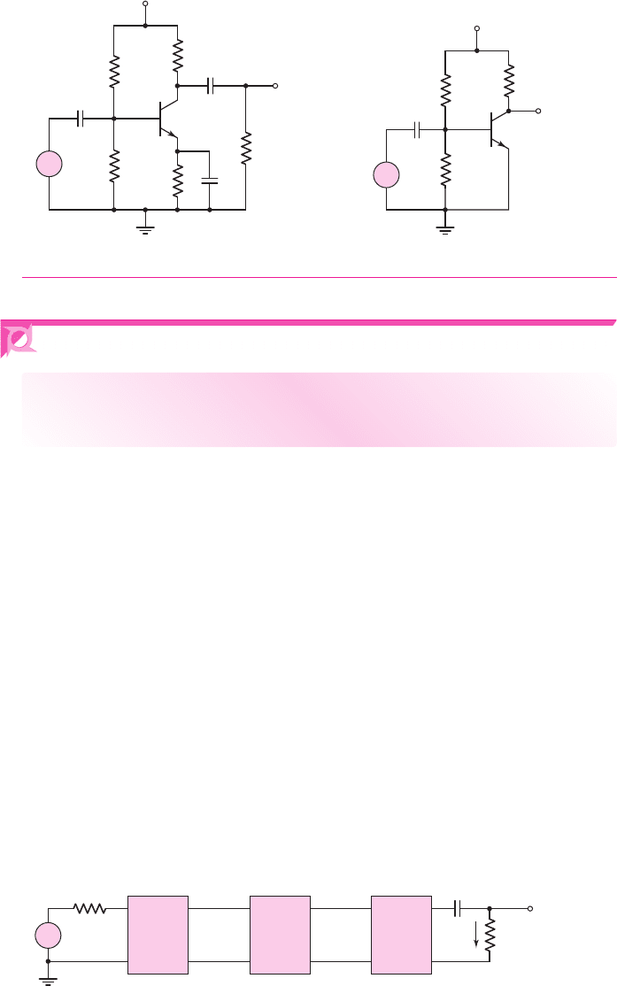
6.11 DESIGN APPLICATION: AUDIO AMPLIFIER
Objective: • Design a bipolar transistor audio amplifier to meet a set
of specifications.
Specifications: An audio amplifier is to deliver an average power of 0.1 W to an
8
speaker from a microphone that produces a 10 mV peak sinusoidal signal and has a
source resistance of
10 k
.
Design Approach: A direct, perhaps brute force, approach will be taken in this
design. The generalized multistage amplifier configuration that will be designed is
shown in Figure 6.76. An input buffer stage, which will be an emitter-follower
circuit, is to be used to reduce the loading effect of the
10 k
source resistance. The
output stage will also be an emitter-follower circuit to provide the necessary out-
put current and output signal power. The gain stage will actually be composed of a
2-stage common-emitter amplifier that will provide the necessary voltage gain. We
will assume that the entire amplifier system is biased with a 12 volt power supply.
Solution (Input Buffer Stage): The input buffer stage, an emitter-follower
amplifier, is shown in Figure 6.77. We will assume that the transistor has a current
gain of
β
1
= 100
. We will design the circuit so that the quiescent collector current
is
I
CQ1
= 1
mA, the quiescent collector-emitter voltage is
V
CEQ1
= 6
V, and
R
1
R
2
= 100 k
.
Q
v
o
v
s
R
L
= 2 kΩ
R
C
=
2 kΩ
V
CC
= +12 V
R
E
=
0.5 kΩ
R
2
=
30 kΩ
R
1
=
125 kΩ
C
E
C
C2
C
C1
+
–
Figure 6.74 Figure for Exercise TYU 6.18
Q
v
O
v
s
R
C
V
CC
= +5 V
R
2
=
10 kΩ
R
1
= 53.8 kΩ
C
C1
+
–
Figure 6.75 Figure for Exercise TYU 6.19
+
–
R
L
= 8 Ω
R
s
= 10 kΩ
v
i
i
L
v
o
Buffer
stage
Gain
stage
Output
stage
Figure 6.76 Generalized multistage amplifier for design application
nea80644_ch06_369-468.qxd 06/13/2009 07:32 PM Page 445 F506 Hard disk:Desktop Folder:Rakesh:MHDQ134-06:
446 Part 1 Semiconductor Devices and Basic Applications
We find
R
E1
∼
=
V
CC
− V
CEQ1
I
CQ1
=
12 − 6
1
= 6k
We obtain
r
π1
=
β
1
V
T
I
CQ1
=
(100)(0.026)
1
= 2.6k
We also have, neglecting the loading effect of the next stage,
R
i1
= R
1
R
2
[r
π1
+(1 +β
1
)R
E1
]
= 100[2.6 +(101)(6)] = 85.9k
The small-signal voltage gain, from Equation (6.68) and assuming that
r
o
=∞
,is
(again neglecting the loading effect from the next stage)
A
v1
=
v
o1
v
i
=
(1 + β
1
)R
E1
r
π1
+(1 +β
1
)R
E1
·
R
i1
R
i1
+ R
S
=
(101)(6)
2.6 + (101)(6)
·
85.9
85.9 + 10
or
A
v1
= 0.892
For a 10 mV peak input signal voltage, the peak voltage at the output of the buffer
stage is now
v
o1
= 8.92
mV.
We find the bias resistors to be
R
1
= 155 k
and
R
2
= 282 k
.
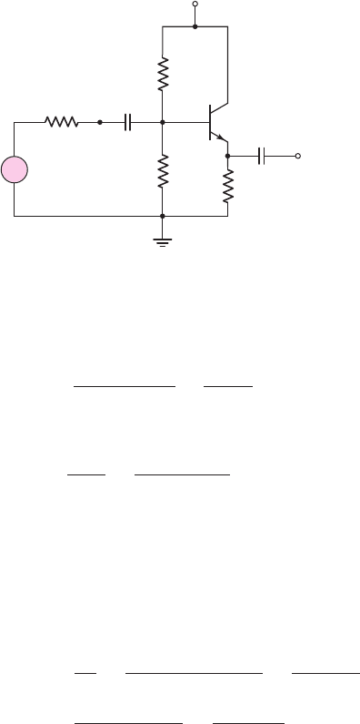
Solution (Output Stage): The output stage, another emitter-follower amplifier cir-
cuit, is shown in Figure 6.78. The
8
speaker is capacitively coupled to the output of the
amplifier. The coupling capacitor ensures that no dc current flows through the speaker.
For an average power of 0.1 W to be delivered to the load, the rms value of the
load current is found from
P
L
= i
2
L
(rms) · R
L
or
0.1 = i
2
L
(rms) · 8
which yields
i
L
(rms) = 0.112 A
. For a sinusoidal signal, the peak output current is then
i
L
(peak) = 0.158 A
v
o1
v
i
R
s
= 10 kΩ
Q
1
V
CC
= 12 V
R
E1
R
2
R
1
+
–
Figure 6.77 Input signal source and input buffer stage (emitter-follower) for design
application
nea80644_ch06_369-468.qxd 06/13/2009 07:32 PM Page 446 F506 Hard disk:Desktop Folder:Rakesh:MHDQ134-06:
Chapter 6 Basic BJT Amplifiers 447
and the peak output voltage is
v
o
(peak) = (0.158)(8) = 1.26 V
We will assume that the output power transistor has a current gain of
β
4
= 50
.
We will set the quiescent transistor parameters at
I
EQ4
= 0.3 A and V
CEQ4
= 6V
Then
R
E4
=
V
CC
− V
CEQ4
I
EQ4
=
12 − 6
0.3
= 20
We find
I
CQ4
=
β
4
1 + β
4
· I
EQ4
=
50
51
(0.3) = 0.294 A
Then
r
π4
=
β
4
V
T
I
CQ4
=
(50)(0.026)
0.294
= 4.42
The small-signal voltage gain of the output stage is
A
v4
=
v
o
v
o3
=
(1 + β
4
)(R
E4
R
L
)
r
π4
+(1 +β
4
)(R
E4
R
L
)
=
(51)(208)
4.42 + (51)(208)
= 0.985
which is very close to unity, as we would expect. For a required peak output voltage
of
v
o
= 1.26
V, we then need a peak voltage at the output of the gain stage to be
v
o3
= 1.28
V.
Solution (Gain Stage): The gain stage, which will actually be a two-stage
common-emitter amplifier, is shown in Figure 6.79. We will assume that the buffer
stage is capacitively coupled to the input of the amplifier, the two stages of the am-
plifier are capacitively coupled, and the output of this amplifier is directly coupled to
the output stage.
V
CC
= 12 V
R
i4
V
B4
Q
4
I
B4
R
E4
v
o3
v
o
R
L
= 8 Ω
i
L
Figure 6.78 Output stage (emitter-follower) for design application
nea80644_ch06_369-468.qxd 06/13/2009 07:32 PM Page 447 F506 Hard disk:Desktop Folder:Rakesh:MHDQ134-06: