Neamen D. Microelectronics: Circuit Analysis and Design
Подождите немного. Документ загружается.


428 Part 1 Semiconductor Devices and Basic Applications
The output resistance, given by Equation (6.79), is
R
o
=
r
π
+ R
1
R
2
R
S
1 + β
R
E
r
o
The first term, with (
1 + β
) in the denominator, dominates, and if
R
1
R
2
R
S
∼
=
R
S
,
then we have
R
o
∼
=
r
π
+ R
S
1 + β
For
R
o
= 200
, we find
0.2 =
r
π
+10
101
or
r
π
= 10.2k
. Since
r
π
= (β V
T
)/I
CQ
, the quiescent collector current must be
I
CQ
=
βV
T
r
π
=
(100)(0.026)
10.2
= 0.255 mA
Assuming
I
CQ
∼
=
I
EQ
and letting
V
CEQ
= 5
V, we find
R
E
=
V
+
− V
CEQ
− V
−
I
EQ
=
5 − 5 −(−5)
0.255
= 19.6k
The term
(1 + β)R
E
is
(1 + β)R
E
= (101)(19.6) ⇒ 1.98 M
With this large resistance, we can design a bias-stable circuit as defined in Chapter 5
and still have large values for bias resistances. Let
R
TH
= (0.1)(1 +β)R
E
= (0.1)(101)(19.6) = 198 k
The base current is
I
B
=
V
TH
− V
BE
(on) − V
−
R
TH
+(1 +β)R
E
where
V
TH
=
R
2
R
1
+ R
2
(10) − 5 =
1
R
1
(R
TH
)(10) − 5
We can then write
0.255
100
=
1
R
1
(198)(10) − 5 −0.7 −(−5)
198 + (101)(19.6)
We find
R
1
= 317 k
and
R
2
= 527 k
.
Comment: The quiescent collector current
I
CQ
= 0.255
mA establishes the re-
quired
r
π
value which in turn establishes the required output resistance R
o
.
Trade-offs: We will investigate the effects of a variation in transistor current gain.
In this example, we will assume that the designed resistor values are available.
nea80644_ch06_369-468.qxd 06/13/2009 07:32 PM Page 428 F506 Hard disk:Desktop Folder:Rakesh:MHDQ134-06:
Chapter 6 Basic BJT Amplifiers 429
The Thevenin equivalent resistance is
R
TH
= R
1
R
2
= 198 k
and the
Thevenin equivalent voltage is
V
TH
= 1.244
V. The base current is found by the
KVL equation around the B–E loop. We find
I
BQ
=
1.244 − 0.7 −(−5)
198 + (1 +β)(19.6)
The collector current is
I
CQ
= β I
BQ
and we find
r
π
= (β V
T
)/I
CQ
.
Finally, the out-
put resistance is approximately
R
o
∼
=
r
π
+ R
TH
R
S
1 + β
=
r
π
+19810
1 + β
The values of these parameters for several values of
β
are shown in the following
table.
From these results, we see that the specified maximum output resistance of
R
o
∼
=
200
is met only if the current gain of the transistor is at least
β = 100
. In this de-
sign, then, we must specify that the minimum current gain of a transistor is 100.
Computer Simulation: We again used approximation techniques in our design. For
this reason, it is useful to verify our design with a PSpice analysis, since the computer
simulation will take into account more details than our hand design.
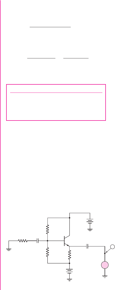
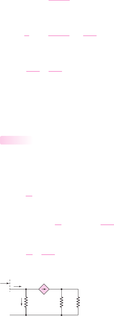
Figure 6.56 shows the PSpice circuit schematic diagram. A 1 mV sinusoidal
signal source is capacitively coupled to the output of the emitter follower. The input
signal source has been set equal to zero. The current from the output signal source
was found to be 5.667
μ
A. The output resistance of the emitter follower is then
R
o
= 176
, which means that we have met our desired specification that the output
resistance should be less than
200
.
β I
CQ
(mA) r
π
(k) R
o
()
50 0.232 5.62 297
75 0.246 7.91 229
100 0.255 10.2 195
125 0.260 12.5 175
+
–
~
0
0
0
v
3
1 mV
0
10 kΩ
467 kΩ
344 kΩ
2N3904
19.6 kΩ
C
3
R
1
Q
1
C
2
–5 V
+
–
5 V
+
–
R
2
R
E
R
S
V
–
V
+
100 mF
100 mF
I
Figure 6.56 PSpice circuit schematic for Example 6.14
nea80644_ch06_369-468.qxd 06/13/2009 07:32 PM Page 429 F506 Hard disk:Desktop Folder:Rakesh:MHDQ134-06:
V
–
= –10 V
V
+
= +10 V
v
s
R
S
R
ib
C
C1
C
C2
v
o
C
R
B
=
100 kΩ
R
E
=
10 kΩ
R
L
R
o
R
C
= 10 kΩ
i
i
i
o
+
–
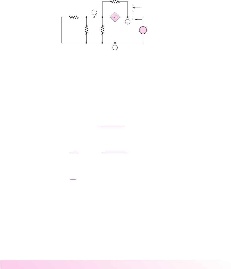
Figure 6.57 Figure for Exercise TYU 6.10
430 Part 1 Semiconductor Devices and Basic Applications
Discussion: From the computer simulation, the quiescent collector current is
I
CQ
= 0.239 mA
compared to the designed value of
I
CQ
= 0.255 mA
. The principal
reason for the difference in value is the difference in base-emitter voltage and current
gain between the hand analysis and computer simulation.
The output resistance specification is met in the computer simulation. In the
PSpice analysis, the ac beta is 135 and the output resistance is
R
o
= 176
. This
value correlates very well with the hand analysis in which
R
o
= 184
for
β = 125
.
EXERCISE PROBLEM
Ex 6.14: For the circuit in Figure 6.54, the transistor parameters are:
β = 100
,
V
BE
(on) = 0.7
V, and
V
A
= 125
V. Assume
R
S
= 0
and
R
L
=
1 k
. (a) Design a
bias-stable circuit such that
I
CQ
= 1.25
mA and
V
CEQ
= 4
V. (b) What is the
small-signal current gain
A
i
= i
o
/i
i
? (c) What is the output resistance looking
back into the output terminals? (Ans. (a)
R
E
= 4.76
k
,
R
1
= 65.8
k
,
R
2
= 178.8
k
; (b)
A
i
= 29.9
, (c)
R
o
= 20.5
)
Test Your Understanding
TYU 6.10 Assume the circuit in Figure 6.57 uses a 2N2222 transistor. Assume a
nominal dc current gain of
β = 130
. Using the average h-parameter values (assume
h
re
= 0
) given in the data sheets, determine
A
v
= v
o
/v
s
,
A
i
= i
o
/i
s
, R
ib
,
and R
o
for
R
S
= R
L
= 10
k
. (Ans.
A
v
= 0.891
,
A
i
= 8.59
,
R
ib
= 641
k
,
R
o
= 96
)
TYU 6.11 For the circuit in Figure 6.58,
R
E
= 2k
,
R
1
= R
2
= 50 k
and the
transistor parameters are
β = 100
,
V
EB
(on) = 0.7
V, and
V
A
= 125
V. (a) Determine
the small-signal voltage gain
A
v
= v
o
/v
s
. (b) Find the resistances R
ib
and R
o
.
(Ans. (a)
A
v
= 0.925
, (b)
R
ib
= 4.37 k
,
R
o
= 32.0
)
TYU 6.12 The parameters of the circuit shown in Figure 6.57 are
V
+
= 3.3
V,
V
−
=−3.3
V,
R
E
= 15
k
,
R
L
= 2
k
,
R
S
= 2
k
, and
R
C
= 0
. The transistor
parameters are
β = 120
and
V
A
=∞
. (a) Determine the quiescent values
I
EQ
and
nea80644_ch06_369-468.qxd 06/13/2009 08:24 PM Page 430 F506 Hard disk:Desktop Folder:Rakesh:MHDQ134-06:
Chapter 6 Basic BJT Amplifiers 431
V
CEQ
. (b) Find the small-signal voltage gain and small-signal current gain.
(c) Calculate the small-signal input resistance
R
ib
and the small-signal output
resistance
R
o
. (Ans. (a)
I
EQ
= 0.163
mA,
V
CEQ
= 4.14
V; (b)
A
v
= 0.892
,
A
i
= 32.1
; (c)
R
ib
= 232.7
k
,
R
o
= 172 )
6.7 COMMON-BASE AMPLIFIER
Objective: • Analyze the common-base amplifier and become familiar
with the general characteristics of this circuit.
A third amplifier circuit configuration is the common-base circuit. To determine the
small-signal voltage and current gains, and the input and output impedances, we will
use the same hybrid-
π
equivalent circuit for the transistor that was used previously.
The dc analysis of the common-base circuit is essentially the same as for the
common-emitter circuit.
Small-Signal Voltage and Current Gains
Figure 6.59 shows the basic common-base circuit, in which the base is at signal
ground and the input signal is applied to the emitter. Assume a load is connected to
the output through a coupling capacitor C
C2
.
6.7.1
R
2
R
1
R
E
v
s
V
CC
= +5 V
C
C1
C
C2
v
o
R
ib
R
o
R
L
=
500 Ω
i
i
i
o
+
–
Figure 6.58 Figure for Exercises TYU 6.11.
+
–
V
CC
+
–
V
EE
v
s
R
S
C
C1
C
C2
i
o
R
B
R
E
C
B
R
C
v
o
R
L
+
–
Figure 6.59 Basic common-base circuit. The input signal is applied to the emitter terminal
and the output signal is measured at the collector terminal.
nea80644_ch06_369-468.qxd 06/13/2009 07:32 PM Page 431 F506 Hard disk:Desktop Folder:Rakesh:MHDQ134-06:
432 Part 1 Semiconductor Devices and Basic Applications
Figure 6.60(a) again shows the hybrid-
π
model of the npn transistor, with the
output resistance r
o
assumed to be infinite. Figure 6.60(b) shows the small-signal
equivalent circuit of the common-base circuit, including the hybrid-
π
model of the
transistor. As a result of the common-base configuration, the hybrid-
π
model in the
small-signal equivalent circuit may look a little strange.
The small signal output voltage is given by
V
o
=−(g
m
V
π
)(R
C
R
L
)
(6.86)
Writing a KCL equation at the emitter node, we obtain
g
m
V
π
+
V
π
r
π
+
V
π
R
E
+
V
s
−(−V
π
)
R
S
= 0
(6.87)
Since
β = g
m
r
π
, Equation (6.87) can be written
V
π
1 + β
r
π
+
1
R
E
+
1
R
S
=−
V
s
R
S
(6.88)
Then,
V
π
=−
V
s
R
S
r
π
1 + β
R
E
R
S
(6.89)
Substituting Equation (6.89) into (6.86), we find the small-signal voltage gain, as
follows:
A
v
=
V
o
V
s
=+g
m
R
C
R
L
R
S
r
π
1 + β
R
E
R
S
(6.90)
We can show that as R
S
approaches zero, the small-signal voltage gain becomes
A
v
= g
m
(R
C
R
L
)
(6.91)
Figure 6.60(b) can also be used to determine the small-signal current gain. The
current gain is defined as
A
i
= I
o
/I
i
. Writing a KCL equation at the emitter node, we
have
I
i
+
V
π
r
π
+ g
m
V
π
+
V
π
R
E
= 0
(6.92)
Solving for
V
π
, we obtain
V
π
=−I
i
r
π
1 + β
R
E
(6.93)
(a)
(b)
+
–
V
p
R
C
R
L
V
s
R
E
r
p
I
i
R
S
I
o
I
b
V
o
E C
B
g
m
V
p
+
–
+
–
V
p
g
m
V
p
r
p
I
b
E
CB
Figure 6.60 (a) Simplified hybrid-
π
model of the npn transistor and (b) small-signal
equivalent circuit of the common-base circuit
nea80644_ch06_369-468.qxd 06/13/2009 07:32 PM Page 432 F506 Hard disk:Desktop Folder:Rakesh:MHDQ134-06:
Chapter 6 Basic BJT Amplifiers 433
The load current is given by
I
o
=−(g
m
V
π
)
R
C
R
C
+ R
L
(6.94)
Combining Equations (6.93) and (6.94), we obtain an expression for the small-signal
current gain, as follows:
A
i
=
I
o
I
i
= g
m
R
C
R
C
+ R
L
r
π
1 + β
R
E
(6.95)
If we take the limit as R
E
approaches infinity and R
L
approaches zero, then the
current gain becomes the short-circuit current gain given by
A
io
=
g
m
r
π
1 + β
=
β
1 + β
= α
(6.96)
where
α
is the common-base current gain of the transistor.
Equations (6.90) and (6.96) indicate that, for the common-base circuit, the
small-signal voltage gain is usually greater than 1 and the small-signal current gain
is slightly less than 1. However, we still have a small-signal power gain. The appli-
cations of a common-base circuit take advantage of the input and output resistance
characteristics.
Input and Output Impedance
Figure 6.61 shows the small-signal equivalent circuit of the common-base configura-
tion looking into the emitter. In this circuit, for convenience only, we have reversed
the polarity of the control voltage, which reverses the direction of the dependent cur-
rent source.
The input resistance looking into the emitter is defined as
R
ie
=
V
π
I
i
(6.97)
If we write a KCL equation at the input, we obtain
I
i
= I
b
+ g
m
V
π
=
V
π
r
π
+ g
m
V
π
= V
π
1 + β
r
π
(6.98)
Therefore,
R
ie
=
V
π
I
i
=
r
π
1 + β
≡ r
e
(6.99)
6.7.2
+
–
V
p
R
C
R
L
g
m
V
p
r
p
I
i
R
ie
I
b
Figure 6.61 Common-base equivalent circuit for input resistance calculations
nea80644_ch06_369-468.qxd 06/13/2009 07:32 PM Page 433 F506 Hard disk:Desktop Folder:Rakesh:MHDQ134-06:
434 Part 1 Semiconductor Devices and Basic Applications
The resistance looking into the emitter, with the base grounded, is usually defined as
r
e
and is quite small, as already shown in the analysis of the emitter-follower circuit.
When the input signal is a current source, a small input resistance is desirable.
Figure 6.62 shows the circuit used to calculate the output resistance looking
back into the collector terminal. The small-signal resistance
r
o
is included. The inde-
pendent source
v
s
has been set equal to zero. We may define an equivalent resistance
R
eq
= R
S
R
E
r
π
.
Writing a KCL equation at the output node, we obtain
I
x
= g
m
V
π
+
V
x
−(−V
π
)
r
o
(6.100(a))
A KCL equation at the emitter node yields
V
π
R
eq
+ g
m
V
π
+
V
x
−(−V
π
)
r
o
= 0
(6.100(b))
Combining Equations (6.100(a)) and (6.100(b)), we find that output resistance as
V
x
I
x
= R
oc
= r
o
1 + g
m
R
eq
+ R
eq
(6.101)
If the input resistance
R
S
= 0
, then
R
eq
= 0
and the output resistance is just
given by
R
oc
= r
o
. Including a collector resistor and a load resistor, the output resis-
tance looking back into the output terminal is
R
o
= R
oc
R
C
R
L
.
Since the output resistance looking back into the collector terminal is very large,
the common-base circuit looks almost like an ideal current source. The circuit is also
referred to as a current buffer.
Discussion
The common-base circuit is very useful when the input signal is a current. We will
see this type of application when we discuss the cascode circuit in Section 6.9.
Test Your Understanding
TYU 6.13 For the circuit shown in Figure 6.63, the transistor parameters are:
β = 100
,
V
EB
(on) = 0.7
V, and
r
o
=∞
. (a) Calculate the quiescent values of
I
CQ
and
V
ECQ
. (b) Determine the small-signal current gain
A
i
= i
o
/i
i
. (c) Determine the
small-signal voltage gain
A
v
= v
o
/v
s
. (Ans. (a)
I
CQ
= 0.921
mA,
V
ECQ
= 6.1
V
(b)
A
i
= 0.987
(c)
A
v
= 177
)
+
–
R
S
R
E
r
p
g
m
V
p
R
oc
+
–
V
p
E
C
B
I
x
V
x
r
o
Figure 6.62 Common-base equivalent circuit for output resistance calculations
nea80644_ch06_369-468.qxd 06/13/2009 07:32 PM Page 434 F506 Hard disk:Desktop Folder:Rakesh:MHDQ134-06:
Chapter 6 Basic BJT Amplifiers 435
+
–
V
CC
= 10 V
+
–
V
EE
= 10 V
v
s
C
C
i
o
i
i
R
E
= 10 kΩ R
C
= 5 kΩ
v
o
+
–
Figure 6.63 Figure for Exercise TYU 6.13
+
–
V
CC
+
–
V
EE
v
s
R
S
R
i
C
C1
C
C2
i
o
i
i
R
B
R
E
C
B
R
C
v
o
R
L
R
o
+
–
Figure 6.64 Figure for Exercises TYU 6.14 and TYU 6.15
6.8 THE THREE BASIC AMPLIFIERS:
SUMMARY AND COMPARISON
Objective: • Compare the general characteristics of the three basic
amplifier configurations.
The basic small-signal characteristics of the three single-stage amplifier configura-
tions are summarized in Table 6.4.
For the common-emitter circuit, the voltage and current gains are generally
greater than 1. For the emitter-follower, the voltage gain is slightly less than 1, while
the current gain is greater than 1. For the common-base circuit, the voltage gain is
greater than 1, while the current gain is less than 1.
Table 6.4 Characteristics of the three BJT amplifier configurations
Configuration Voltage gain Current gain Input resistance Output resistance
Common emitter
A
v
> 1 A
i
> 1
Moderate Moderate to high
Emitter follower
A
v
∼
=
1
A
i
> 1
High Low
Common base
A
v
> 1
A
i
∼
=
1
Low Moderate to high
TYU 6.14 The transistor parameters for the circuit shown in Figure 6.64 are
β = 120
,
V
BE
(on) = 0.7
V, and
V
A
=∞
. The circuit parameters are
V
CC
=
V
EE
= 3.3
V,
R
S
= 500
,
R
L
= 6
k
,
R
B
= 100
k
,
R
E
= 12
k
, and
R
C
=
12
k
. (a) Determine the small-signal transistor parameters
g
m
,
r
π
, and
r
o
. (b) Find
the small-signal current gain
A
i
= i
o
/i
i
and the small-signal voltage gain
A
v
= v
o
/v
s
.
(c) Determine the input resistance
R
i
and the output resistance
R
o
. (Ans. (a)
g
m
=
7.73
mA/V,
r
π
= 15.5
k
,
r
o
=∞
; (b)
A
i
= 0.654
,
A
v
= 6.26
; (c)
R
i
= 127
,
R
o
= 12
k
)
TYU 6.15 For the circuit shown in Figure 6.64, let
R
S
= 0
,
C
B
= 0
,
R
C
= R
L
=
2k
,
V
CC
= V
EE
= 5
V,
β = 100
,
V
BE
(on) = 0.7
V, and
V
A
=∞
. Design R
E
and
R
B
for a dc quiescent collector current of 1 mA and a small-signal voltage gain of 20.
(Ans.
R
B
= 2.4k
,
R
E
= 4.23 k
)
nea80644_ch06_369-468.qxd 06/13/2009 07:32 PM Page 435 F506 Hard disk:Desktop Folder:Rakesh:MHDQ134-06:
436 Part 1 Semiconductor Devices and Basic Applications
The input resistance looking into the base terminal of a common-emitter circuit
may be in the low kilohm range; in an emitter follower, it is generally in the 50 to
100 k
range. The input resistance looking into the emitter of a common-base circuit
is generally on the order of tens of ohms.
The overall input resistance of both the common-emitter and emitter-follower
circuits can be greatly affected by the bias circuitry.
The output resistance of the emitter follower is generally in the range of a few
ohms to tens of ohms. In contrast, the output resistance looking into the collector ter-
minal of the common-emitter and common-base circuits is very high. In addition, the
output resistance looking back into the output terminal of the common-emitter and
common-base circuits is a strong function of the collector resistance. For these cir-
cuits, the output resistance can easily drop to a few kilohms.
The characteristics of these single-stage amplifiers will be used in the design of
multistage amplifiers.
6.9 MULTISTAGE AMPLIFIERS
Objective: • Analyze multitransistor or multistage amplifiers and
understand the advantages of these circuits over single-transistor
amplifiers.
In most applications, a single transistor amplifier will not be able to meet the
combined specifications of a given amplification factor, input resistance, and output
resistance. For example, the required voltage gain may exceed that which can be
obtained in a single transistor circuit. We also saw an illustration of this effect in
Example 6.14, in which a low output resistance was required in a particular design.
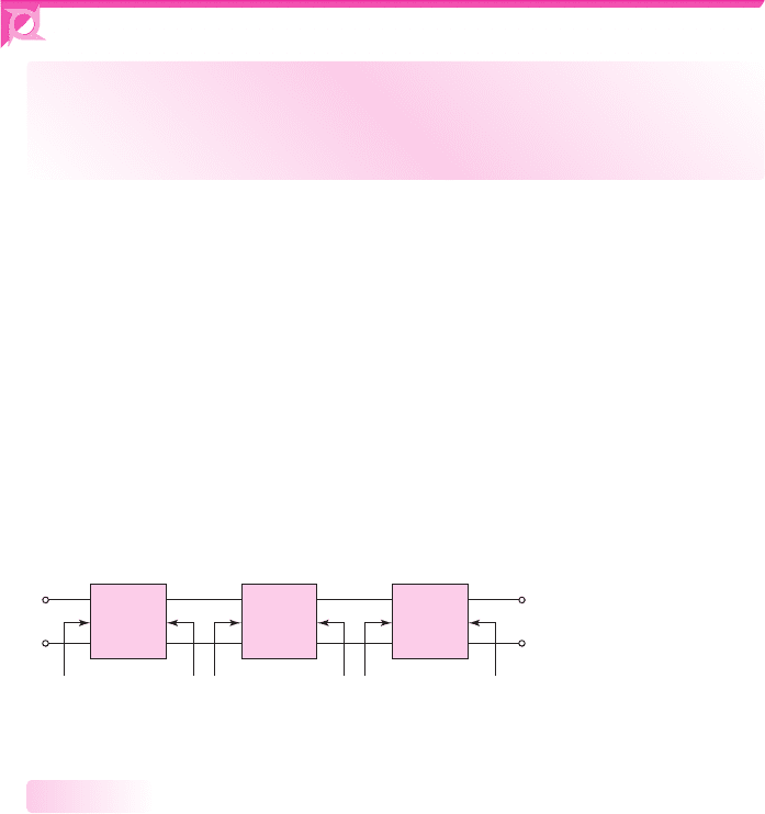
Transistor amplifier circuits can be connected in series, or cascaded, as shown in
Figure 6.65. This may be done either to increase the overall small-signal voltage gain
or to provide an overall voltage gain greater than 1, with a very low output resistance.
The overall voltage or current gain, in general, is not simply the product of the individ-
ual amplification factors. For example, the gain of stage 1 is a function of the input re-
sistance of stage 2. In other words, loading effects may have to be taken into account.
There are many possible multistage configurations; we will examine a few here,
in order to understand the type of analysis required.
+
–
v
s
R
i1
R
o1
R
i2
R
o2
R
i3
R
o3
+
–
v
o
Stage 1
A
V1
Stage 2
A
V 2
Stage 3
A
V3
Figure 6.65 A generalized three-stage amplifier
Multistage Analysis: Cascade Configuration
In Figure 6.66, the circuit is a cascade configuration of two common-emitter circuits.
The dc analysis of this circuit, done in Example 5.19 of Chapter 5, showed that both
transistors are biased in the forward-active mode. Figure 6.67 shows the small-signal
6.9.1
nea80644_ch06_369-468.qxd 06/13/2009 07:32 PM Page 436 F506 Hard disk:Desktop Folder:Rakesh:MHDQ134-06:
Chapter 6 Basic BJT Amplifiers 437
equivalent circuit, assuming all capacitors act as short circuits and each transistor
output resistance r
o
is infinite.
We may start the analysis at the output and work back to the input, or start at the
input and work toward the output.
The small-signal voltage gain is
A
v
=
V
o
V
s
= g
m1
g
m2
(R
C1
r
π2
)(R
C2
R
L
)
R
i
R
i
+ R
S
(6.102)
The input resistance of the amplifier is
R
i
= R
1
R
2
r
π1
which is identical to that of a single-stage common-emitter amplifier. Similarly, the
output resistance looking back into the output terminals is
R
o
= R
C2
. To determine
the output resistance, the independent source V
s
is set equal to zero, which means that
V
π1
= 0
. Then
g
m1
V
π1
= 0
, which gives
V
π2
= 0
and
g
m 2
V
π 2
= 0
. The output
resistance is therefore
R
C2
. Again, this is the same as the output resistance of a
single-stage common-emitter amplifier.
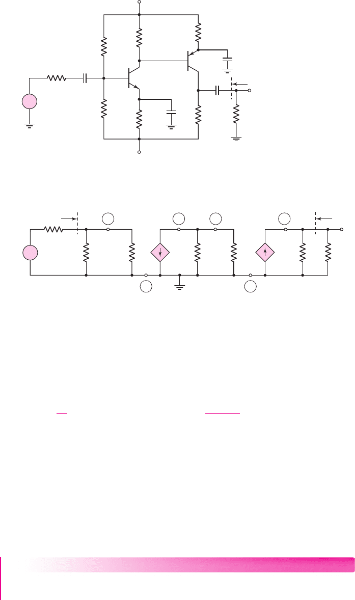
COMPUTER EXAMPLE 6.15
Objective: Determine the small-signal voltage gain of the multitransistor circuit
shown in Figure 6.66 using a PSpice analysis.
R
2
=
50 kΩ
R
S
= 0.5 kΩ
R
1
=
100 kΩ
R
C1
= 5 kΩ
R
E2
= 2 kΩ
R
E1
=
2 kΩ
v
s
V
–
= –5 V
C
C1
C
C2
V
+
= +5 V
v
o
C
E1
C
E2
R
C2
=
1.5 kΩ
R
L
=
5 kΩ
Q
1
Q
2
R
o
+
–
Figure 6.66 A two-stage common-emitter amplifier in a cascade configuration with npn and
pnp transistors
+
–
V
p1
R
C1
R
S
R
i
R
o
R
C2
R
L
g
m1
V
p1
V
s
V
o
r
p1
r
p 2
g
m2
V
p 2
+
–
V
p 2
R
1
⎜⎜ R
2
B
1
C
1
B
2
C
2
E
1
E
2
+
–
Figure 6.67 Small-signal equivalent circuit of the cascade circuit shown in Figure 6.66
nea80644_ch06_369-468.qxd 06/13/2009 07:32 PM Page 437 F506 Hard disk:Desktop Folder:Rakesh:MHDQ134-06: