Neamen D. Microelectronics: Circuit Analysis and Design
Подождите немного. Документ загружается.


498 Part 1 Semiconductor Devices and Basic Applications
EXAMPLE 7.7
Objective: Determine the corner frequencies and limiting horizontal asymptotes of
a common-emitter circuit with an emitter bypass capacitor.
Consider the circuit in Figure 7.27(a) with parameters
R
E
= 4k
,
R
C
= 2k
,
R
S
= 0.5k
,
C
E
= 1 μ
F,
V
+
= 5
V, and
V
−
=−5
V. The transistor parameters
are:
β = 100
,
V
BE
(on) = 0.7
V, and
r
o
=∞
.
Solution: From the dc analysis, we find the quiescent collector current as
I
CQ
= 1.06
mA. The small-signal parameters are
g
m
= 40.77
mA/V,
r
π
= 2.45 k
,
and
r
o
=∞
.
The time constant
τ
A
is
τ
A
= R
E
C
E
= (4 ×10
3
)(1 × 10
−6
) = 4 ×10
−3
s
and the time constant
τ
B
is
τ
B
=
R
E
(R
S
+r
π
)C
E
[R
S
+r
π
+(1 +β)R
E
]
=
(4 × 10
3
)(0.5 × 10
3
+2.45 ×10
3
)(1 × 10
−6
)
[0.5 × 10
3
+2.45 ×10
3
+(101)(4 ×10
3
)]
or
τ
B
= 2.90 ×10
−5
s
The corner frequencies are then
f
A
=
1
2πτ
A
=
1
2π(4 ×10
−3
)
= 39.8Hz
and
f
B
=
1
2πτ
B
=
1
2π(2.9 ×10
−5
)
⇒ 5.49 kHz
The limiting low-frequency horizontal asymptote, given by Equation (7.61(a)) is
A
v
ω→0
=
g
m
r
π
R
C
[R
S
+r
π
+(1 +β)R
E
]
=
(40.8)(2.45)(2)
[0.5 + 2.45 +(101)(4)]
= 0.491
The limiting high-frequency horizontal asymptote, given by Equation (7.61(b)) is
A
v
ω→∞
=
g
m
r
π
R
C
R
S
+r
π
=
(40.77)(2.45)(2)
0.5 + 2.45
= 67.7
Comment: Comparing the two limiting values of voltage gain, we see that including
a bypass capacitor produces a large high-frequency gain.
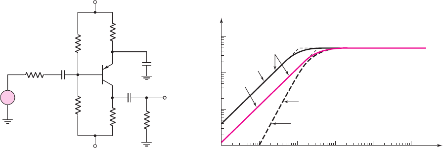
Computer Verification: The results of a PSpice analysis are given in Figure 7.29.
The magnitude of the small-signal voltage gain is shown in Figure 7.29(a). The two
corner frequencies are approximately 39 Hz and 5600 Hz, which agree very well
with the results from the time constant analysis. The two limiting magnitudes of 0.49
and 68 also correlate extremely well with the hand analysis results.
Figure 7.29(b) is a plot of the phase response versus frequency. At very low and
very high frequencies, where the capacitor acts as either an open circuit or short
nea80644_ch07_469-558.qxd 06/13/2009 08:07 PM Page 498 F506 Hard disk:Desktop Folder:Rakesh:MHDQ134-07:
Chapter 7 Frequency Response 499
circuit, the phase is
−180
degrees, as expected for a common-emitter circuit.
Between the two corner frequencies, the phase changes substantially, approaching
−90
degrees.
11010
2
10
3
10
4
10
5
0.1
1.0
10
100
f (Hz)
|A
V
|
(a)
(b)
1
10
3
10
2
10 10
4
10
5
–90
Phase
–100
–110
–120
–130
–140
–150
–160
–170
–180
f (Hz)
Figure 7.29 PSpice analysis results for the circuit with an emitter bypass capacitor:
(a) voltage gain magnitude response and (b) phase response
EXERCISE PROBLEM
Ex 7.7: The circuit shown in Figure 7.27(a) has parameters
V
+
= 10
V,
V
−
=−10
V,
R
S
= 0.5k
,
R
E
= 4k
, and
R
C
= 2k
. The transistor parame-
ters are:
V
BE
(on) = 0.7
V,
V
A
=∞
, and
β = 100
. (a) Determine the value of C
E
such that the low-frequency 3 dB point is
f
B
= 200
Hz. (b) Using the results from
part (a), determine f
A
. (Ans. (a)
C
E
= 49.5 μ
F, (b)
f
A
= 0.80
Hz)
The analysis of an FET amplifier with a source bypass capacitor is essentially
the same as for the bipolar circuit. The general form of the voltage gain expression
is the same as Equation (7.60), and the Bode plot of the gain is essentially the same
as that shown in Figure 7.28.
Combined Effects: Coupling and Bypass Capacitors
When a circuit contains multiple capacitors, the frequency response analysis be-
comes more complex. In many amplifier applications, the circuit is to amplify an
7.3.5
nea80644_ch07_469-558.qxd 06/13/2009 08:07 PM Page 499 F506 Hard disk:Desktop Folder:Rakesh:MHDQ134-07:
500 Part 1 Semiconductor Devices and Basic Applications
R
S
= 0.1 kΩ
C
C1
C
E
v
o
R
E
= 10 kΩ
R
C
=
5 kΩ
R
L
= 2 kΩ
R
1
= 320 kΩ
R
2
= 280 kΩ
C
C2
v
s
+
–
+10 V
–10 V
Figure 7.30 Circuit with two coupling capacitors
and an emitter bypass capacitor
f (Hz)
6 dB/octave
12 dB/octave
C
2
= 2
m
F
10
2
1010.1
10
3
10
4
0.1
1
10
100
|A
V
|
C
1
= 1
m
F
C
2
= 2
m
F
C
1
= 1
m
F
Figure 7.31 PSpice results for each coupling capacitor, and the
combined effect for the circuit in Figure 7.30
(C
E
→∞)
input signal whose frequency is confined to the midband range. In this case, the
actual frequency response outside the midband range is not of interest. The end
points of the midband range are defined to be those frequencies at which the gain de-
creases by 3 dB from the maximum midband value. These endpoint frequencies are
a function of the high- and low-frequency capacitors. These capacitors introduce a
pole to the amplifier transfer function.
If multiple coupling capacitors, for example, exist in a circuit, one capacitor may
introduce the pole that produces the 3 dB reduction in the maximum gain at the low
frequency. This pole is referred to as the dominant pole. A more detailed discussion
of dominant poles is given in Chapter 12. A zero-value time constant analysis can be
used to estimate the dominant pole in a circuit containing multiple capacitors. At this
point in the text, we will determine the frequency response of circuits containing
multiple capacitors with a computer simulation.
As an example, Figure 7.30 shows a circuit with two coupling capacitors and an
emitter bypass capacitor, all of which affect the circuit response at low frequencies.
We could develop a transfer function that includes all the capacitors, but the analysis
of such circuits is most easily handled by computer.
Figure 7.31 is the Bode plot of the voltage gain magnitude for the example
circuit, taking into account the effects of the two coupling capacitors. In this case,
the bypass capacitor is assumed to be a short circuit. The plots consider C
1
and C
2
individually, as well as together. As expected, with two capacitors both acting at
the same time, the slope is 40 dB/decade or 12 dB/octave. Since the poles are not
far apart, in the actual circuit, we cannot consider the effect of each capacitor
individually.
Figure 7.32 is the Bode plot of the voltage gain magnitude, taking into account
the emitter bypass capacitor and the two coupling capacitors. The plot shows the ef-
fect of the bypass capacitor, the effect of the two coupling capacitors, and the net ef-
fect of the three capacitors together. When all three capacitors are taken into account,
the slope is continually changing; there is no definitive corner frequency. However,
at approximately
f = 150
Hz, the curve is 3 dB below the maximum asymptotic
nea80644_ch07_469-558.qxd 06/13/2009 08:07 PM Page 500 F506 Hard disk:Desktop Folder:Rakesh:MHDQ134-07:
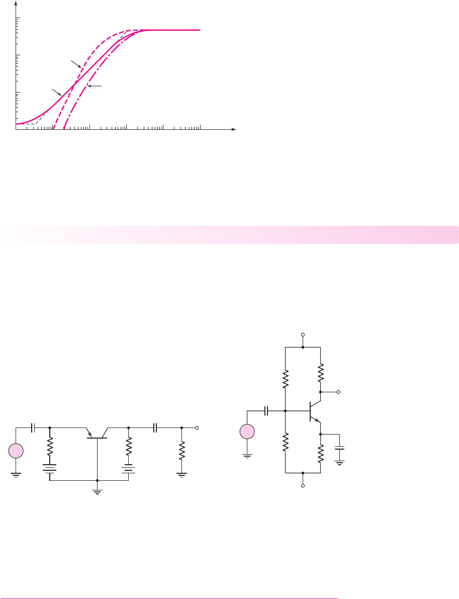
Chapter 7 Frequency Response 501
value, and this frequency is defined as the lower corner frequency, or lower cutoff
frequency.
Test Your Understanding
TYU 7.4 Consider the common-base circuit shown in Figure 7.33. Can the two cou-
pling capacitors be treated separately? (a) From a computer analysis, determine the
cutoff frequency. Assume the parameter values are
β = 100
and
I
S
= 2 ×10
−15
A.
(b) Determine the midband small-signal voltage gain. (Ans. (a)
f
3db
= 1.2
kHz,
(b)
A
v
= 118
)
f (Hz)
|A
V
|
10
3
10
4
0.1
1
10
100
C
1
= 1
m
F
C
2
= 2
m
F
C
1
= 1
m
F
C
2
= 2
m
F
C
E
= 50
m
F
C
E
= 50
m
F
10
2
1010.1
Figure 7.32 PSpice results for the two coupling capacitors, the bypass capacitor, and the
combined effects
C
C1
= 4.7
m
F C
C2
= 4.7
m
F
R
E
= 10 kΩ
v
s
R
L
=
10 kΩ
v
o
+
–
+
–
V
EE
= 10 V
R
C
= 5 kΩ
+
–
V
CC
= 10 V
Figure 7.33 Figure for Exercise TYU 7.4
v
O
C
C1
= 1 mF
C
E
= 10 mF
R
C
= 2.3 kΩ
R
1
= 20 kΩ
R
E
=
5 kΩ
+5 V
R
2
=
20 kΩ
–5 V
v
s
+
–
Figure 7.34 Figure for Exercise TYU 7.5
TYU 7.5 The common-emitter circuit shown in Figure 7.34 contains both a coupling
capacitor and an emitter bypass capacitor. (a) From a computer analysis, determine
the 3 dB frequency. Assume the parameter values are
β = 100
and
I
S
=
2 × 10
−15
A
. (b) Determine the midband small-signal voltage gain. (Ans. (a)
f
3dB
≈
575 Hz, (b)
|A
v
|
max
= 74.4
)
nea80644_ch07_469-558.qxd 06/13/2009 08:07 PM Page 501 F506 Hard disk:Desktop Folder:Rakesh:MHDQ134-07:
502 Part 1 Semiconductor Devices and Basic Applications
7.4 FREQUENCY RESPONSE:
BIPOLAR TRANSISTOR
Objective: • Determine the frequency response of the bipolar tran-
sistor, and determine the Miller effect and Miller capacitance.
Thus far, we have considered the frequency response of circuits as a function of
external resistors and capacitors, and we have assumed the transistor to be ideal.
However, both bipolar transistors and FETs have internal capacitances that influence
the high-frequency response of circuits. In this section, we will first develop an
expanded small-signal hybrid-
π
model of the bipolar transistor, taking these
capacitances into account. We will then use this model to analyze the frequency
characteristics of the bipolar transistor.
Expanded Hybrid-π Equivalent Circuit
When a bipolar transistor is used in a linear amplifier circuit, the transistor is biased
in the forward-active region, and small sinusoidal voltages and currents are superim-
posed on the dc voltages and currents. Figure 7.35(a) shows an npn bipolar transistor
in a common-emitter configuration, along with the small-signal voltages and
currents. Figure 7.35(b) is a cross section of the npn transistor in a classic integrated
circuit configuration. The C, B, and E terminals are the external connections to the
transistor, and the C
,B
, and E
points are the idealized internal collector, base, and
emitter regions.
To construct the equivalent circuit of the transistor, we will first consider various
pairs of terminals. Figure 7.36(a) shows the equivalent circuit for the connection be-
tween the external base input terminal and the external emitter terminal. Resistance
r
b
is the base series resistance between the external base terminal B and the internal
base region
B
. The
B
–E
junction is forward biased; therefore,
C
π
is the forward-
biased junction capacitance and
r
π
is the forward-biased junction diffusion resis-
tance. Both parameters are functions of the junction current. Finally, r
ex
is the emitter
series resistance between the external emitter terminal and the internal emitter
region. This resistance is usually very small, on the order of 1 to 2
.
Figure 7.36(b) shows the equivalent circuit looking into the collector terminal.
Resistance r
c
is the collector series resistance between the external and internal
7.4.1
+
–
V
ce
B
C
E
n
+
buried layer
n
n
p
p
p
CB E BC
E'
B'
C'
(a) (b)
I
b
I
c
+
–
V
be
Figure 7.35 (a) Common-emitter npn bipolar transistor with small-signal currents and
voltages and (b) cross section of an npn bipolar transistor, for the hybrid-
π
model
nea80644_ch07_469-558.qxd 06/13/2009 08:07 PM Page 502 F506 Hard disk:Desktop Folder:Rakesh:MHDQ134-07:
Chapter 7 Frequency Response 503
collector connections, and capacitance C
s
is the junction capacitance of the reverse-
biased collector–substrate junction. The dependent current source,
g
m
V
π
, is the tran-
sistor collector current controlled by the internal base–emitter voltage. Resistance r
o
is the inverse of the output conductance g
o
and is due primarily to the Early effect.
Finally, Figure 7.36(c) shows the equivalent circuit of the reverse-biased
B
–C
junction. Capacitance
C
μ
is the reverse-biased junction capacitance, and
r
μ
is the
reverse-biased diffusion resistance. Normally,
r
μ
is on the order of megohms and can
be neglected. The value of
C
μ
is usually much smaller than
C
π
; however, because of
a phenomenon known as the Miller effect,
C
μ
usually cannot be neglected. (We will
consider the Miller effect later in this chapter.)
The complete hybrid-
π
equivalent circuit for the bipolar transistor is shown in
Figure 7.37. The capacitances lead to frequency effects in the transistor. One result is
that the gain is a function of the input signal frequency. Because of the large number
of elements, a computer simulation of this complete model is easier than a hand
analysis. However, we can make some simplifications in order to evaluate some
fundamental frequency effects of bipolar transistors.
Short-Circuit Current Gain
We can begin to understand the frequency effects of the bipolar transistor by first
determining the short-circuit current gain, after simplifying the hybrid-
π
model.
7.4.2
(a) (b) (c)
r
b
r
ex
C
p
r
p
+
–
V
p
B'
B
E'
E
r
c
r
o
C'
C
E'
C
s
g
m
V
p
r
m
B' C
'
C
m
Figure 7.36 Components of the hybrid-
π
equivalent circuit: (a) base to emitter, (b) collector
to emitter, and (c) base to collector
g
m
V
p
r
o
r
ex
r
b
r
c
r
p
C
p
+
–
V
p
r
m
B'
E
E'
B
C'
C
C
m
C
s
Figure 7.37 Hybrid-
π
equivalent circuit
nea80644_ch07_469-558.qxd 06/13/2009 08:07 PM Page 503 F506 Hard disk:Desktop Folder:Rakesh:MHDQ134-07:
504 Part 1 Semiconductor Devices and Basic Applications
Figure 7.38 shows a simplified equivalent circuit for the transistor, in which we ne-
glect the parasitic resistances r
b
, r
c
, and
r
ex
, the B–C diffusion resistance
r
μ
, and the
substrate capacitance C
s
. Also, the collector is connected to signal ground. Keep in
mind that the transistor must still be biased in the forward-active region. We will
determine the small-signal current gain
A
i
= I
c
/I
b
.
Writing a KCL equation at the input node, we find that
I
b
=
V
π
r
π
+
V
π
1
jωC
π
+
V
π
1
jωC
μ
= V
π
1
r
π
+ jω(C
π
+C
μ
)
(7.63)
We see that
V
π
is no longer equal to
I
b
r
π
, since a portion of I
b
is now shunted through
C
π
and
C
μ
.
From a KCL equation at the output node, we obtain
V
π
1
jωC
μ
+ I
c
= g
m
V
π
(7.64(a))
or
I
c
= V
π
(g
m
− jωC
μ
)
(7.64(b))
The input voltage
V
π
can then be written as
V
π
=
I
c
(g
m
− jωC
μ
)
(7.64(c))
Substituting this expression for
V
π
into Equation (7.63) yields
I
b
= I
c
·
1
r
π
+ jω(C
π
+C
μ
)
(g
m
− jωC
μ
)
(7.65)
The small-signal current gain usually designated as
h
fe
, becomes
A
i
=
I
c
I
b
= h
fe
=
(g
m
− jωC
μ
)
1
r
π
+ jω(C
π
+C
μ
)
(7.66)
If we assume typical circuit parameter values of
C
μ
= 0.05
pF,
g
m
= 50
mA/V,
and a maximum frequency of
f = 500
MHz, then we see that
ωC
μ
g
m
. There-
fore, to a good approximation, the small-signal current gain is
h
fe
∼
=
g
m
1
r
π
+ jω(C
π
+C
μ
)
=
g
m
r
π
1 + jωr
π
(C
π
+C
μ
)
(7.67)
r
p
C
p
g
m
V
p
C
m
CB
E
r
o
I
b
I
c
+
–
V
p
Figure 7.38 Simplified hybrid-
π
equivalent circuit for determining the short-circuit
current gain
nea80644_ch07_469-558.qxd 06/13/2009 08:07 PM Page 504 F506 Hard disk:Desktop Folder:Rakesh:MHDQ134-07:

Chapter 7 Frequency Response 505
Since
g
m
r
π
= β
, then the low frequency current gain is just
β
, as we previously
assumed. Equation (7.67) shows that, in a bipolar transistor, the magnitude and phase
of the current gain are both functions of the frequency.
Figure 7.39(a) is a Bode plot of the short-circuit current gain magnitude. The
corner frequency, which is also the beta cutoff frequency
f
β
in this case, is given by
f
β
=
1
2πr
π
(C
π
+C
μ
)
(7.68)
Figure 7.39(b) shows the phase of the current gain. As the frequency increases,
the small-signal collector current is no longer in phase with the small-signal base cur-
rent. At high frequencies, the collector current lags the input current by 90 degrees.
(a)
(b)
0
Phase
–45°
–90°
f
b
f
f
b
f
T
f
3 dB
b
o
1
|h
fe
|
Figure 7.39 Bode plots for the short-circuit current gain: (a) magnitude and (b) phase
EXAMPLE 7.8
Objective: Determine the 3 dB frequency of the short-circuit current gain of a bipo-
lar transistor.
Consider a bipolar transistor with parameters
r
π
= 2.6k
,
C
π
= 0.5
pF,
and
C
μ
= 0.025
pF.
Solution: From Equation (7.68), we find
f
β
=
1
2πr
π
(C
π
+C
μ
)
=
1
2π(2.6 ×10
3
)(0.5 + 0.025)(10
−12
)
or
f
β
= 117 MHz
Comment: High-frequency transistors must have small capacitances; therefore,
small devices must be used.
EXERCISE PROBLEM
Ex 7.8: A bipolar transistor has parameters
β
o
= 120
,
C
μ
= 0.02
pF, and
f
β
=
90
MHz and is biased at
I
CQ
= 0.2
mA. (a) Determine
C
π
. (b) What is the
magnitude of the short-circuit current gain at (i)
f = 50
MHz, (ii)
f = 125
MHz,
and (iii)
f = 500
MHz. (Ans. (a)
C
π
= 0.093
pF; (b) (i) 105, (ii) 70.1, (iii) 21.3)
nea80644_ch07_469-558.qxd 06/13/2009 08:07 PM Page 505 F506 Hard disk:Desktop Folder:Rakesh:MHDQ134-07:
506 Part 1 Semiconductor Devices and Basic Applications
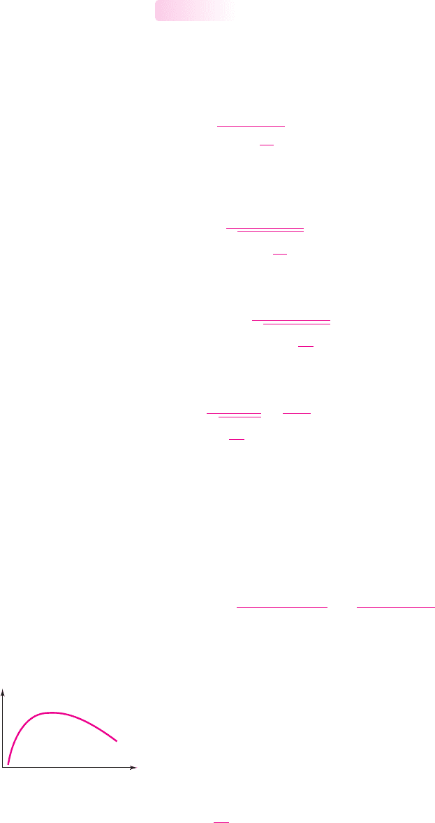
f
T
I
C
Figure 7.40 Cutoff
frequency versus collector
current
Cutoff Frequency
Figure 7.39(a) shows that the magnitude of the small-signal current gain decreases
with increasing frequency. At frequency
f
T
, which is the cutoff frequency, this gain
goes to 1. The cutoff frequency is a figure of merit for transistors.
From Equation (7.67), we can write the small-signal current gain in the form
h
fe
=
β
o
1 + j
f
f
β
(7.69)
where
f
β
is the beta cutoff frequency defined by Equation (7.68). The magnitude of
h
fe
is
h
fe
=
β
o
1 +
f
f
β
2
(7.70)
At the cutoff frequency
f
T
,
|h
fe
|=1
, and Equation (7.70) becomes
h
fe
= 1 =
β
o
1 +
f
T
f
β
2
(7.71)
Normally,
β
o
1
, which implies that
f
T
f
β
. Then Equation (7.71) can be written as
1
∼
=
β
o
f
T
f
β
2
=
β
o
f
β
f
T
(7.72(a))
or
f
T
= β
o
f
β
(7.72(b))
Frequency
f
β
is also called the bandwidth of the transistor. Therefore, from
Equation (7.72(b)), the cutoff frequency f
T
is the gain–bandwidth product of the tran-
sistor, or more commonly the unity-gain bandwidth. From Equation (7.68), the
unity-gain bandwidth is
f
T
= β
o
1
2πr
π
(C
π
+C
μ
)
=
g
m
2π(C
π
+C
μ
)
(7.73)
Since the capacitances are a function of the size of the transistor, we see again that
high frequency transistors imply small device sizes.
The cutoff frequency f
T
is also a function of the dc collector current I
C
, and the gen-
eral characteristic of f
T
versus I
C
is shown in Figure 7.40. The transconductance g
m
is
directly proportional to I
C
, but only a portion of
C
π
is related to I
C
. The cutoff frequency
is therefore lower at low collector current levels. However, the cutoff frequency also de-
creases at high current levels, in the same way that β decreases at large currents.
The cutoff frequency or unity-gain bandwidth of a transistor is usually specified
on the device data sheets. Since the low-frequency current gain is also given, the beta
cutoff frequency, or bandwidth, of the transistor can be determined from
f
β
=
f
T
β
o
(7.74)
7.4.3
nea80644_ch07_469-558.qxd 06/13/2009 08:07 PM Page 506 F506 Hard disk:Desktop Folder:Rakesh:MHDQ134-07:

Chapter 7 Frequency Response 507
The cutoff frequency of the general-purpose 2N2222A discrete bipolar transis-
tor is
f
T
= 300 MHz
. For the MSC3130 discrete bipolar transistor, which has a spe-
cial surface mount package, the cutoff frequency is
f
T
= 1.4 GHz
. This tells us that
very small transistors fabricated in integrated circuits can have cutoff frequencies in
the low GHz range.
EXAMPLE 7.9
Objective: Calculate the bandwidth
f
β
and capacitance
C
π
of a bipolar transistor.
Consider a bipolar transistor that has parameters
f
T
= 20
GHz at
I
C
= 1
mA,
β
o
= 120
, and
C
μ
= 0.08
pF.
Solution: From Equation (7.74), we find the bandwidth as
f
β
=
f
T
β
o
=
20 × 10
9
120
→
f
β
= 167 MHz
The transconductance is
g
m
=
I
C
V
T
=
1
0.026
= 38.46 mA/V
The
C
π
capacitance is determined from Equation (7.73). We have
f
T
=
g
m
2π(C
π
+C
μ
)
or
20 × 10
9
=
38.5 × 10
−3
2π(C
π
+0.08 ×10
−12
)
which yields
C
π
= 0.226 pF
.
Comment: Although the value of
C
π
may be much larger than that of
C
μ
,
C
μ
can-
not be neglected in circuit applications as we will see in the next section.
EXERCISE PROBLEM
Ex 7.9: A BJT is biased at
I
C
= 0.15
mA, and has parameters
β
o
= 150
,
C
π
= 0.8
pF, and
C
μ
= 0.012
pF. Determine
f
β
and
f
T
. (Ans.
f
β
= 7.54
MHz,
f
T
= 1.13
GHz)
The hybrid-π equivalent circuit for the bipolar transistor uses discrete or lumped
elements. However, when cutoff frequencies are on the order of
f
T
∼
=
1
0 GHz and
the transistor is operated at microwave frequencies, other parasitic elements and dis-
tributed parameters must be included in the transistor model. For simplicity, we will
assume in this text that the hybrid-
π
model is sufficient to model the transistor char-
acteristics up through the beta cutoff frequency.
Miller Effect and Miller Capacitance
As previously mentioned, the
C
μ
capacitance cannot in reality be ignored. The Miller
effect, or feedback effect, is a multiplication effect of
C
μ
in circuit applications.
7.4.4
nea80644_ch07_469-558.qxd 06/13/2009 08:07 PM Page 507 F506 Hard disk:Desktop Folder:Rakesh:MHDQ134-07: