Neamen D. Microelectronics: Circuit Analysis and Design
Подождите немного. Документ загружается.

678 Part 2 Analog Electronics
9.52 (a) Assume the op-amp in the circuit in Figure P9.52 is ideal. Determine
i
L
as a function of
v
I
. (b) Let
R
1
= 9k
and
R
L
= 1k
. If the op-amp satu-
rates at
±10 V
, determine the maximum value of
v
I
and
i
L
before the op-
amp saturates.
9.53 Consider the three circuits shown in Figure P9.53. Determine each output
voltage for (i)
v
I
= 3
V and (ii)
v
I
=−5
V.
Section 9.5 Op-Amp Applications
*9.54 A current-to-voltage converter is shown in Figure P9.54. The current source
has a finite output resistance R
S
, and the op-amp has a finite open-loop
differential gain A
od
. (a) Show that the input resistance is given by
R
in
=
R
F
1 + A
od
(b) If
R
F
= 10 k
and
A
od
= 1000
, determine the range of
R
S
such that the
output voltage deviates from its ideal value by less than 1 percent.
–
+
R
1
R
2
+
–
–
+
R
R
–
+
v
I
v
O2
v
O1
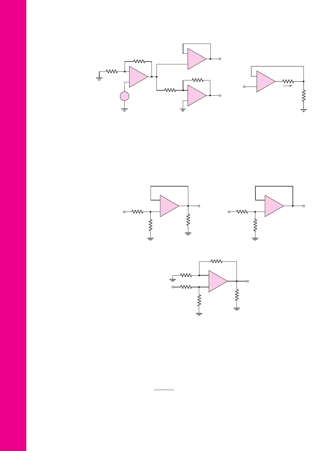
Figure P9.51
R
1
R
L
–
+
v
I
i
L
Figure P9.52
+
–
40 kΩ
20 kΩ
10 kΩ
v
O
v
I
+
–
10 kΩ
10 kΩ
6 kΩ
5 kΩ
48 kΩ
v
O
v
I
(a) (b)
(
c
)
40 kΩ
20 kΩ
v
O
v
I
+
–
Figure P9.53
nea80644_ch09_619-686.qxd 6/19/09 4:26 AM Page 678 pmath DATA-DISK:Desktop Folder:18.6.09:MHDQ134-09:
Chapter 9 Ideal Operational Amplifiers and Op-Amp Circuits 679
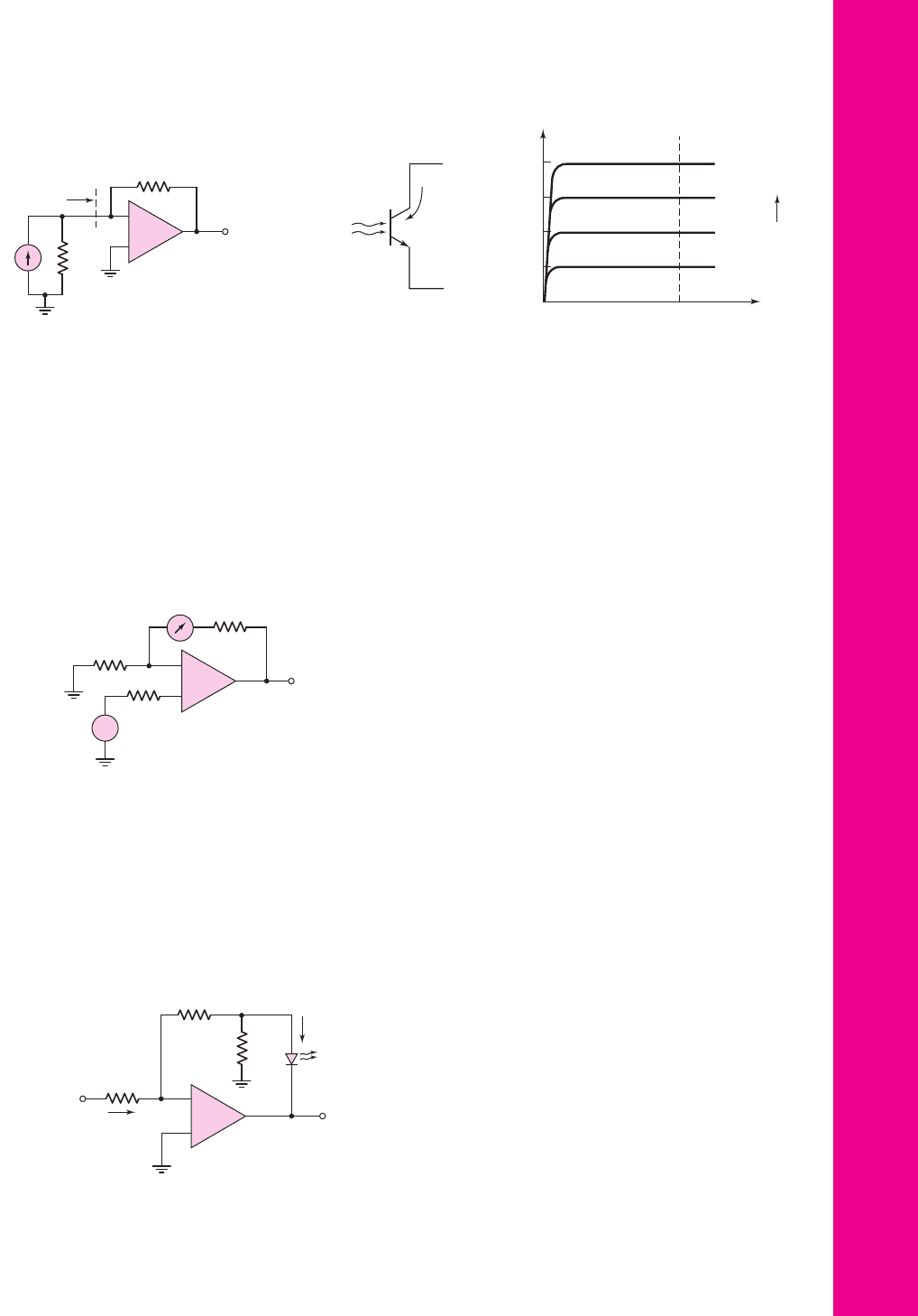
*D9.55 Figure P9.55 shows a phototransistor that converts light intensity into an out-
put current. The transistor must be biased as shown. The transistor output ver-
sus input characteristics are shown. Design a current-to-voltage converter to
produce an output voltage between 0 and 8 V for an input light intensity be-
tween 0 and 20 mW/cm
2
. Power supplies of
+10 V
and
−10 V
are available.
D9.56 The circuit in Figure P9.56 is an analog voltmeter in which the meter read-
ing is directly proportional to the input voltage
v
I
. Design the circuit such
that a 1 mA full-scale reading corresponds to
v
I
= 10 V
. Resistance
R
2
cor-
responds to the meter resistance, and
R
1
corresponds to the source resis-
tance. How do these resistances influence the design?
D9.57 Consider the voltage-to-current converter in Figure 9.22 using an ideal op-
amp. (a) Design the circuit such that the current in a 200
load can be varied
between 0 and 5 mA with an input voltage between 0 and
−5
V. Assume the
op-amp is biased at
±15
V. (b) Using the results of part (a), determine voltage
v
O
; currents
i
2
,
i
3
,
i
4
; and the output current of the op-amp for
v
I
=−5
V.
D9.58 The circuit in Figure P9.58 is used to drive an LED with a voltage source. The
circuit can also be thought of as a current amplifier in that, with the proper
–
+
R
F
R
S
i
S
v
O
R
in
Figure P9.54
Light
intensity,
I (mW/cm
2
)
v
CE
(V)
I (mW/cm
2
)
8
6
4
2
20
15
10
10 V
+
–
5
10
i
C
(mA)
i
C
Figure P9.55
R
R
2
R
1
v
O
v
I
+
–
+
–
Figure P9.56
+
–
R
F
i
D
Ligh
t
v
I
R
1
i
1
R
2
v
O
Figure P9.58
nea80644_ch09_619-686.qxd 6/19/09 4:26 AM Page 679 pmath DATA-DISK:Desktop Folder:18.6.09:MHDQ134-09:

680 Part 2 Analog Electronics
design,
i
D
> i
1
. (a) Derive the expression for
i
D
in terms of
i
1
and the resis-
tors. (b) Design the circuit such that
i
D
= 12 mA
and
i
1
= 1mA
for
v
I
= 5V
.
*9.59 Figure P9.59 is used to calculate the resistance seen by the load in the volt-
age-to-current converter given in Figure 9.22. (a) Show that the output
resistance is given by
R
o
=
R
1
R
2
R
3
R
1
R
3
− R
2
R
F
(b) Using the parameters given in Example 9.5, determine
R
o
. Is this result
unexpected?
(c) Consider the design specification given by Equation (9.44). What is the
expected value of
R
o
?
+
–
R
F
R
o
R
1
R
2
R
3
v
O
Figure P9.59
D9.60 Consider the op-amp difference amplifier in Figure 9.24(a). Let
R
1
= R
3
and
R
2
= R
4
. A load resistor
R
L
= 10
k
is connected from the output ter-
minal to ground. (a) Design the circuit such that the difference voltage gain
is
A
d
= 15
and the minimum difference input resistance is 30 k
. (b) If the
load current is
i
L
= 0.25
mA, what is the differential input voltage
(
v
I2
−v
I1
)
? (c) If
v
I1
= 1.5
V and
v
I2
= 1.2
V, determine
i
L
. (d) If
i
L
= 0.5
mA when
v
I2
= 2.0
V, determine
v
I1
.
D9.61 Consider the differential amplifier shown in Figure 9.24(a). Let
R
1
= R
3
and
R
2
= R
4
. Design the amplifier such that the differential voltage gain is
(a) 40, (b) 25, (c) 5, and (d) 0.5. In each case the differential input resistance
should be as large as possible but under the condition that the largest resis-
tor value is limited to
250 k
.
*9.62 Consider the differential amplifier shown in Figure 9.24(a). Assume that
each resistor is
50(1 ± x) k
. (a) Determine the worst case common-mode
gain
A
CM
= v
O
/v
CM
, where
v
CM
= v
1
= v
2
. (b) Evaluate
A
CM
and
CMRR(dB) for
x = 0.01
, 0.02, and 0.05.
9.63 Let
R = 10
k
in the differential amplifier in Figure P9.63. Determine the
voltages
v
X
,
v
Y
,
v
O
and the currents
i
1
,
i
2
,
i
3
,
i
4
for input voltages of
(a)
v
1
= 1.80
V,
v
2
= 1.40
V; (b)
v
1
= 3.20
V,
v
2
= 3.60
V; and (c)
v
1
=
−1.20
V,
v
2
=−1.35
V.
9.64 Consider the circuit shown in Figure P9.64. (a) The output current of the
op-amp is 1.2 mA and the transistor current gain is
β = 75
. Determine
the resistance
R
. (b) Repeat part (a) if the current is 0.2 mA and the tran-
sistor current gain is
β = 100
. (c) Using the results of part (a), determine
nea80644_ch09_619-686.qxd 6/19/09 4:26 AM Page 680 pmath DATA-DISK:Desktop Folder:18.6.09:MHDQ134-09:
Chapter 9 Ideal Operational Amplifiers and Op-Amp Circuits 681
the op-amp output current if the input voltage is 6 V. (d) Using the
results of part (b), determine the op-amp output current if the input volt-
age is 4 V.
*9.65 The circuit in Figure P9.65 is a representation of the common-mode and dif-
ferential-input signals to a difference amplifier. The output voltage can be
written as
v
O
= A
d
v
d
+ A
cm
v
cm
where
A
d
is the differential-mode gain and
A
cm
is the common-mode gain.
(a) Setting
v
d
= 0
, show that the common-mode gain is given by
A
cm
=
R
4
R
3
−
R
2
R
1
(1 + R
4
/R
3
)
(b) Determine
A
cm
if
R
1
= 10.4
k
,
R
2
= 62.4
k
,
R
3
= 9.6
k
, and
R
4
= 86.4
k
. (c) Determine the maximum value of
|
A
cm
|
if
R
1
=
20
k
±1%
,
R
2
= 80
k
±1%
,
R
3
= 20
k
±1%
, and
R
4
= 80
k
±1%
.
*9.66 Consider the adjustable gain difference amplifier in Figure P9.66. Variable
resistor
R
V
is used to vary the gain. Show that the output voltage
v
O
, as a
function of
v
I1
and
v
I2
, is given by
v
O
=
2R
2
R
1
1 +
R
2
R
V
(v
I2
−v
I1
)
R
10 R
10 R
R
–
+
v
O
v
x
v
y
i
1
i
O
i
3
v
1
v
2
i
2
i
4
Figure P9.63
–
+
+10 V
+25 V
R
Figure P9.64
v
O
R
2
R
1
R
4
R
3
v
I2
–
+
v
cm
v
d/2
v
d/2
v
I1
+
–
+
–
–
+
Figure P9.65
v
O
v
I1
R
1
v
–
v
A
v
B
v
+
v
I2
R
1
R
2
R
2
R
2
R
2
–
+
R
V
Figure P9.66
nea80644_ch09_619-686.qxd 6/19/09 4:26 AM Page 681 pmath DATA-DISK:Desktop Folder:18.6.09:MHDQ134-09:
682 Part 2 Analog Electronics
9.67 Assume the instrumentation amplifier in Figure 9.26 has ideal op-amps. The
circuit parameters are
R
1
= 10
k
,
R
2
= 40
k
,
R
3
= 40
k
, and
R
4
= 120
k
. Determine
v
O1
,
v
O2
,
v
O
, and the current in
R
1
for
(a)
v
I2
= 1.2 +0.08 sin ω t (V), v
I1
= 1.2 −0.08 sin ω t
(V); and (b)
v
I2
=
−0.60 − 0.05 sin ω t
(V),
v
I1
=−0.65 + 0.05 sin ω t
(V).
9.68 Consider the circuit in Figure P9.68. Assume ideal op-amps are used. The
input voltage is
v
I
= 0.5 sin ω t
. Determine the voltages (a)
v
OB
, (b)
v
OC
,
and (c)
v
O
. (d) What is the voltage gain
v
O
/v
I
?
+
–
+
–
+
–
v
OB
+
–
v
OC
+
–
v
I
+
–
v
O
12 kΩ
12 kΩ
12 kΩ
12 kΩ
30 kΩ
40 kΩ
Figure P9.68
R
R
L
i
O
+
–
–
+
v
O1
v
O2
+
–
v
I1
+
–
v
I2
Figure P9.69
9.69 Consider the circuit in Figure P9.69. Assume ideal op-amps are used.
(a) Derive the expression for the current
i
O
as a function of input voltages
v
I1
and
v
I2
. (b) Design the circuit such that
i
O
= 5
mA for
v
I1
= 0.25
V
and
v
I2
=−0.25
V. (c) Using the results of part (b), determine
v
O1
and
v
O2
if
R
L
= 1
k
. (d) Determine
i
O
,
v
O1
, and
v
O2
for
R = 500
,
R
L
= 3
k
,
v
I1
= 1.25
V, and
v
I2
= 1.75
V.
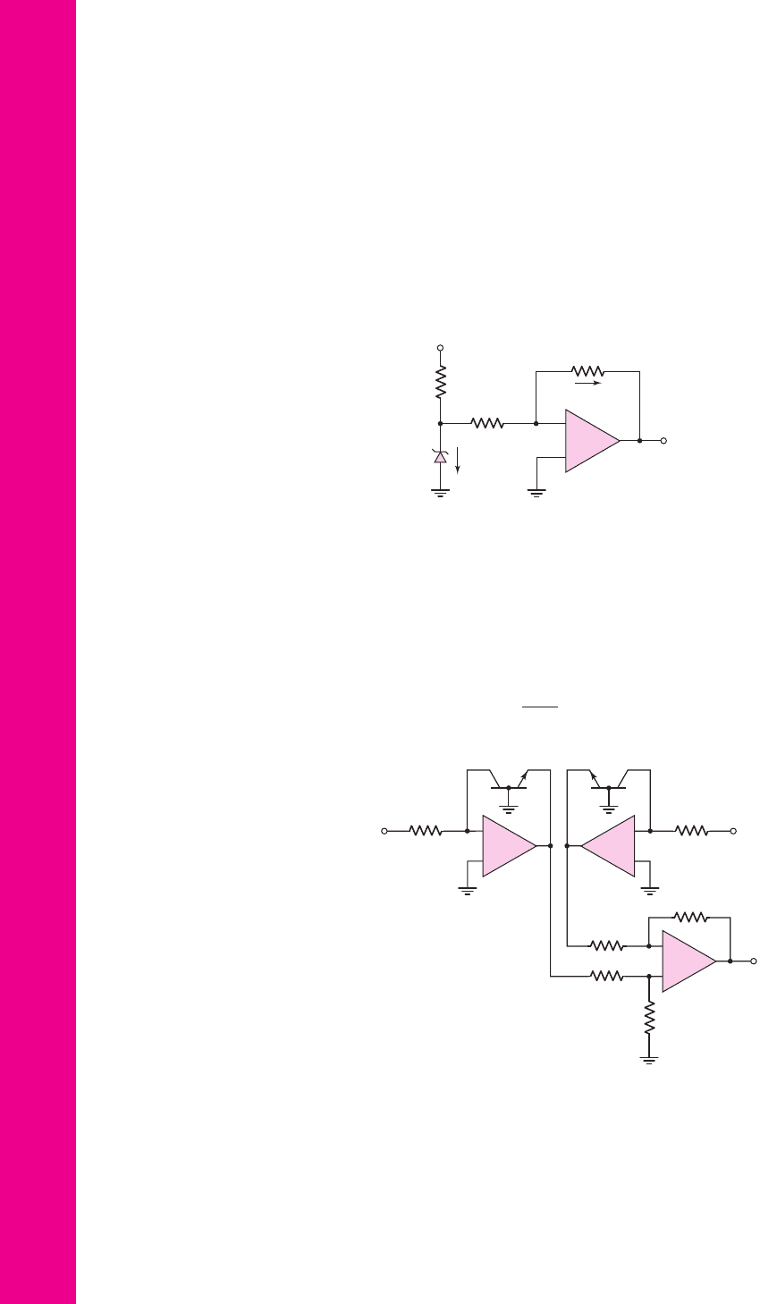
9.70 The instrumentation amplifier in Figure 9.26 has the same circuit parame-
ters and input voltages as given in Problem 9.67, except that
R
1
is replaced
by a fixed resistance
R
1 f
in series with a potentiometer, as shown in Fig-
ure 9.28. Determine the values of
R
1 f
and the potentiometer resistance if
the magnitude of the output has a minimum value of
|
v
O
|
= 0.5V
and a
maximum value of
|
v
O
|
= 8V
.
D9.71 Design the instrumentation amplifier in Figure 9.26 such that the variable
differential voltage gain covers the range of 5 to 200. Set the gain of the dif-
ference amplifier to 2.5. The maximum current in
R
1
is to be limited to
50 μ
A for an output voltage of
10
V. What value of potentiometer is
required?
9.72 All parameters associated with the instrumentation amplifier in Figure 9.26
are the same as given in Exercise Ex 9.8, except that resistor
R
3
, which is
connected to the inverting terminal of A3, is
R
3
= 30 k ± 5%
. Determine
the maximum common-mode gain.
9.73 The parameters in the integrator circuit shown in Figure 9.30 are
R
1
= 20
k
and
C
2
= 0.02 μ
F. The input signal is
v
I
= 0.25 cos ω t
(V).
(a) Determine the frequency at which the input and output signals have
nea80644_ch09_619-686.qxd 6/19/09 4:26 AM Page 682 pmath DATA-DISK:Desktop Folder:18.6.09:MHDQ134-09:
equal amplitudes. At this frequency, what is the phase of the output signal
with respect to the input? (b) At what frequency will the output signal am-
plitude be (i)
|
v
O
|
= 1.5
V and (ii)
|
v
O
|
= 0.15
V?
9.74 Consider the ideal op-amp integrator. Assume the capacitor is initially un-
charged. (a) The output voltage is
v
O
=−5
V at
t = 1.2
s after a
+0.25
V
pulse is applied to the input. What is the RC time constant? (b) Use the re-
sults of part (a). At
t = 1.2
s, the input changes to
−0.10
V. (i) At what time
does
v
O
= 0
? (ii) At what time does
v
O
=+5
V.
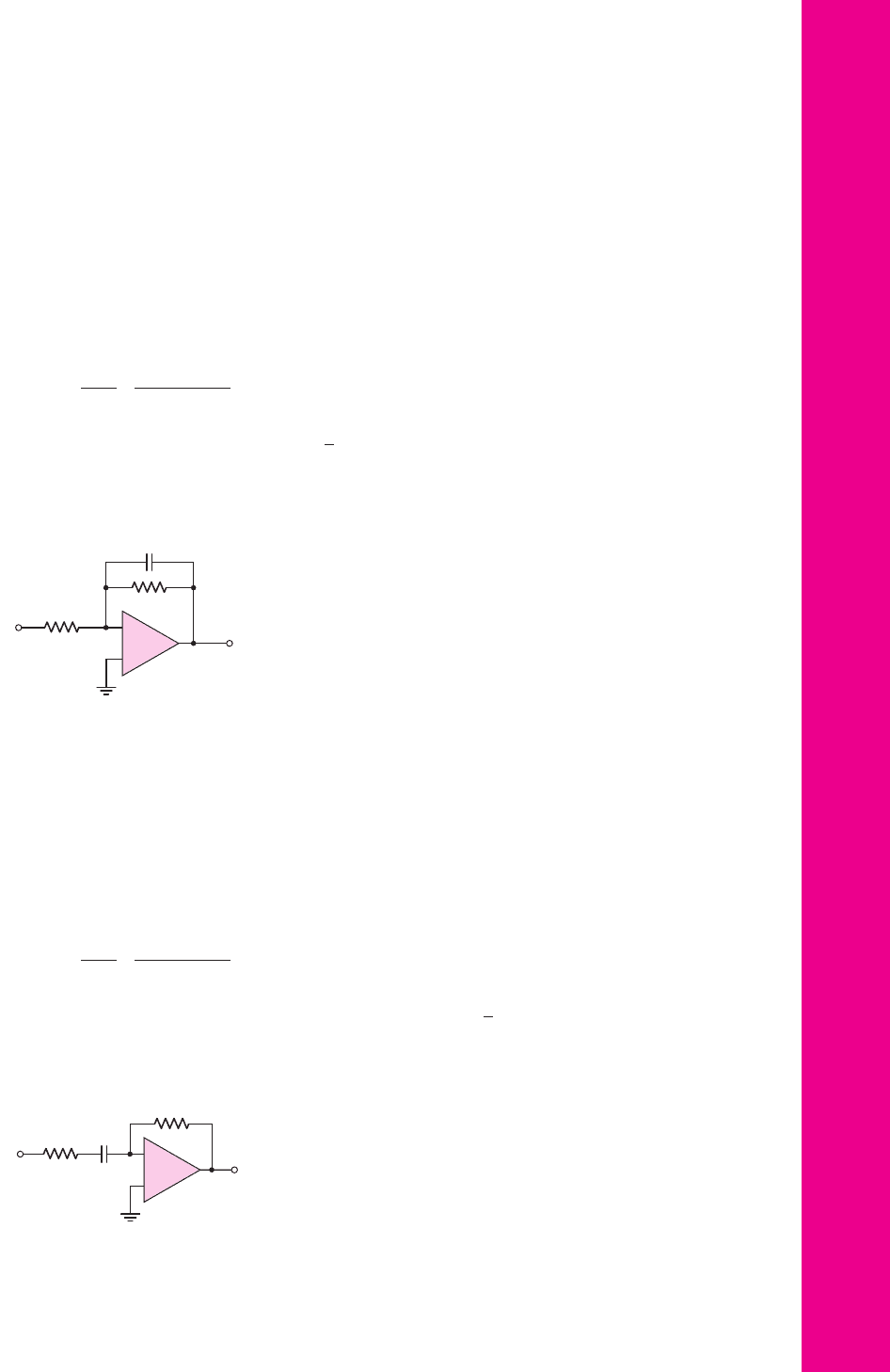
9.75 The circuit in Figure P9.75 is a first-order low-pass active filter. (a) Show
that the voltage transfer function is given by
A
v
=
−R
2
R
1
·
1
1 + jωR
2
C
2
(b) What is the voltage gain at dc (
ω = 0
)? (c) At what frequency is the
magnitude of the voltage gain a factor of
√
2
less that the dc value? (This is
the
−3
dB frequency.)
Chapter 9 Ideal Operational Amplifiers and Op-Amp Circuits 683
v
O
–
+
R
1
R
2
C
2
v
I
Figure P9.75
v
O
v
I
–
+
R
1
R
2
C
1
Figure P9.77
D9.76 (a) Using the results of Problem 9.75, design the low-pass active filter in
Figure P9.75 such that the input resistance is
20
k
, the low-frequency gain
is
−15
, and the
−3
dB frequency is 5 kHz. (b) Repeat part (a) such that the
input resistance is
15
k
, the low-frequency gain is
−25
, and the
−3
dB
frequency is 15 kHz.
9.77 The circuit shown in Figure P9.77 is a first-order high-pass active filter.
(a) Show that the voltage transfer function is given by
A
v
=
−R
2
R
1
·
jωR
1
C
1
1 + jωR
1
C
1
(b) What is the voltage gain as the frequency becomes large?
(c) At what frequency is the magnitude of the gain a factor of
√
2
less than
the high-frequency limiting value?
nea80644_ch09_619-686.qxd 6/19/09 4:26 AM Page 683 pmath DATA-DISK:Desktop Folder:18.6.09:MHDQ134-09:
684 Part 2 Analog Electronics
+10 V
R
S
= 5.6 kΩ
R
1
= 1 kΩ
R
2
= 1 kΩ
i
Z
i
2
v
O
V
Z
= 6.8 V
+
–
+
–
Figure P9.79
D9.78 (a) Using the results of Problem 9.77, design the high-pass active filter in
Figure P9.77 such that the high-frequency voltage gain is
−15
and the
−3
dB frequency is 20 kHz. The maximum resistance value is to be limited
to
350
k
. (b) Repeat part (a) such that the high-frequency gain is
−25
and
the
−3
dB frequency is 35 kHz. The minimum resistance value is to be lim-
ited to
20
k
.
9.79 Consider the voltage reference circuit shown in Figure P9.79. Determine
v
O
,
i
2
, and
i
Z
.
–
+
Q
1
–
+
Q
2
R
2
R
1
333 kΩ
333 kΩ
20 kΩ
20 kΩ
–
+
v
1
v
2
v
O
Figure P9.81
9.80 Consider the circuit in Figure 9.35. The diode parameter is
I
S
= 10
−14
A
and the resistance is
R
1
= 10 k
. Plot
v
O
versus
v
I
over the range
20 mV ≤ v
I
≤ 2V
. (Plot
v
I
on a log scale.)
*9.81 In the circuit in Figure P9.81, assume that
Q
1
and
Q
2
are identical transis-
tors. If
T = 300 K
, show that the output voltage is
v
O
= 1.0 log
10
v
2
R
1
v
1
R
2
9.82 Consider the circuit in Figure 9.36. The diode parameter is
I
S
= 10
−14
A
and the resistance is
R
1
= 10 k
. Plot
v
O
versus
v
I
for
0.30 ≤ v
I
≤
0.60 V
. (Plot
v
O
on a log scale.)
nea80644_ch09_619-686.qxd 6/19/09 4:26 AM Page 684 pmath DATA-DISK:Desktop Folder:18.6.09:MHDQ134-09:
Section 9.7 Op-Amp Circuit Design
*D9.83 Design an op-amp summer to produce the output voltage
v
O
= 2v
I1
−
10v
I2
+3v
I3
−v
I4
. Assume the largest resistor value is
500 k
, and the
input impedance seen by each source is the largest value possible.
*D9.84 Design an op-amp summer to produce an output voltage of
v
O
= 3v
I1
+
1.5v
I2
+2v
I3
−4v
I4
−6v
I5
. The largest resistor value is to be
250
k
.
*D9.85 Design a voltage reference source as shown in Figure 9.42 to have an out-
put voltage of 12.0 V. A Zener diode with a breakdown voltage of 5.6 V is
available. Assume the voltage regulation will be within specifications if the
Zener diode current is within the range of
1.2 ≤ I
Z
≤ 1.35
mA. The start-
up voltage
V
S
is to be 10 V.
*D9.86 Consider the voltage reference circuit in Figure P9.86. Using a Zener diode
with a breakdown voltage of 5.6 V, design the circuit to produce an output
voltage of 12.0 V. Assume the input voltage is 15 V and the Zener diode cur-
rent is
I
Z
= 2
mA.
Chapter 9 Ideal Operational Amplifiers and Op-Amp Circuits 685
V
+
R
1
R
2
R
3
R
T
v
O1
v
O2
Figure P9.87
+
–
+
–
R
1
R
4
R
2
R
L
R
3
V
Z
V
O
V
IN
I
L
I
Z
Figure P9.86
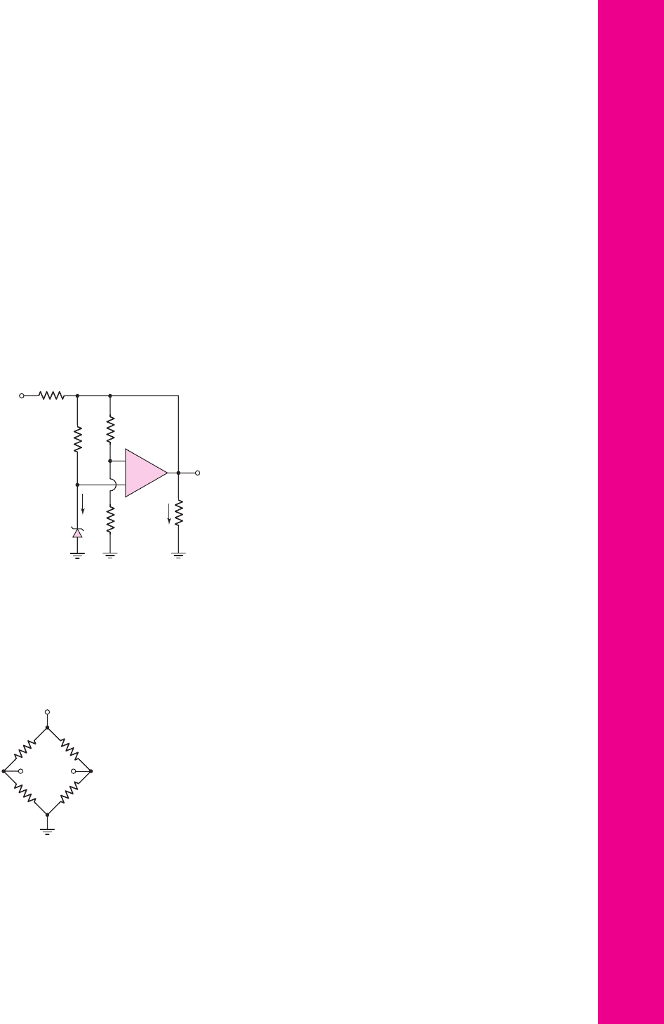
*D9.87 Consider the bridge circuit in Figure P9.87. The resistor
R
T
is a thermistor
with values of
20
k
at
T = 300
K and
21
k
at
T = 350
K. Assume that
the thermistor resistance is linear with temperature, and that the bridge is
biased at
V
+
= 10
V. Design an amplifier system with an output of 0 V at
T = 300
K and 5 V at
T = 350
K.
*D9.88 Consider the bridge circuit in Figure 9.46. The resistance
R
is 20 k
and the
bias is
V
+
= 9
V. (a) Determine
v
O1
as a function of
R
. (b) Design an am-
plifier system such that the output varies from
−5
V to
+5
V as
R
varies
from
+200
to
−200
.
nea80644_ch09_619-686.qxd 6/19/09 4:26 AM Page 685 pmath DATA-DISK:Desktop Folder:18.6.09:MHDQ134-09:

COMPUTER SIMULATION PROBLEMS
9.89 Using a computer simulation, verify the design in Example 9.4.
9.90 Using a computer simulation, verify the design in Example 9.8.
9.91 Using a computer simulation, verify the design in Problem 9.76(b). Plot
v
O
versus frequency over the range
2 ≤ f ≤ 50
kHz.
9.92 Using a computer simulation, verify the design in Problem 9.78(a). Plot
v
O
versus frequency over the range
2 ≤ f ≤ 100
kHz.
DESIGN PROBLEMS
See Design Problems 9.83 to 9.88.
[Note: Each design should be correlated with a computer analysis.]
686 Part 2 Analog Electronics
nea80644_ch09_619-686.qxd 6/19/09 4:26 AM Page 686 pmath DATA-DISK:Desktop Folder:18.6.09:MHDQ134-09:

Chapter
The biasing techniques in Chapters 3 through 6 for FET and BJT amplifiers for the
most part used voltage-divider resistor networks. While this technique can be used for
discrete circuits, it is not suitable for integrated circuits. Resistors require relatively
large areas on an IC compared to transistors; therefore, a resistor-intensive circuit
would necessitate a large chip area.Also, the resistor biasing technique uses coupling
and bypass capacitors extensively. On an IC, it is almost impossible to fabricate
capacitors in the microfarad range, as would be required for the coupling capacitors.
Biasing transistors and transistor circuits in ICs is considerably different from
that in discrete transistor designs. Essentially, biasing integrated circuit amplifiers in-
volves the use of constant-current sources. In this chapter, we will analyze and de-
sign both bipolar and FET circuits that form these constant-current sources. We will
begin to see for the first time in this chapter the use of matched or identical transistor
characteristics as a specific design parameter. Transistors can easily be fabricated in
ICs with matched or identical parameters. A principal goal of this chapter is to help
the reader understand how matched transistor characteristics are used in design and
to be able to design BJT and MOSFET current source circuits.
Transistors are also used as load devices in amplifier circuits. These transistors,
calledactive loads, replace the discrete drain andcollector resistors in FETandBJTcir-
cuits. Using an active load eliminates resistors from the IC and achieves a higher small-
signal voltage gain. The active load is essentially an “upside down” constant-current
source, so an initial discussion of active loads is entirely appropriate in this chapter.
PREVIEW
In this chapter, we will:
• Analyze and understand the characteristics of various bipolar circuits used to
provide a constant output current.
• Analyze and understand the characteristics of various MOSFET (and a few
JFET) circuits used to provide a constant output current.
• Analyze the dc characteristics of amplifier circuits using transistors as load
devices (active loads).
• Analyze the small-signal characteristics of amplifier circuits with active
loads.
• As an application, design an MOS current source circuit to provide a speci-
fied bias current and output resistance.
Integrated Circuit Biasing
and Active Loads
10
10
687
nea80644_ch10_687-752.qxd 6/19/09 4:27 AM Page 687 pmath DATA-DISK:Desktop Folder:18.6.09:MHDQ134-10: