Neamen D. Microelectronics: Circuit Analysis and Design
Подождите немного. Документ загружается.


708 Part 2 Analog Electronics
For the drain current to be independent of the drain-to-source voltage (for
λ = 0
), transistor M
2
should always be biased in the saturation region. The load
current is then
I
O
= K
n2
(V
GS
− V
TN2
)
2
(10.42)
Substituting Equation (10.41) into (10.42), we have
I
O
= K
n2
I
REF
K
n1
+V
TN1
− V
TN2
2
(10.43)
If M
1
and M
2
are identical transistors, then
V
TN1
= V
TN2
and
K
n1
= K
n2
, and Equa-
tion (10.43) becomes
I
O
= I
REF
(10.44)
Since there are no gate currents in MOSFETs, the induced load current is identi-
cal to the reference current, provided the two transistors are matched. The relationship
between the load current and the reference current changes if the width-to-length
ratios, or aspect ratios, of the two transistors change.
If the transistors are matched except for the aspect ratios, we find
I
O
=
(W/L)
2
(W/L)
1
· I
REF
(10.45)
The ratio between the load and reference currents is directly proportional to the
aspect ratios and gives designers versatility in their circuit designs.
Output Resistance
The stability of the load current as a function of the drain-to-source voltage is an im-
portant consideration in many applications. The drain current versus drain-to-source
voltage is similar to the bipolar characteristic shown in Figure 10.4. Taking into ac-
count the finite output resistance of the transistors, we can write the load and refer-
ence currents as follows:
I
O
= K
n2
(V
GS
− V
TN2
)
2
(1 + λ
2
V
DS2
)
(10.46(a))
and
I
REF
= K
n1
(V
GS
− V
TN1
)
2
(1 + λ
1
V
DS1
)
(10.46(b))
Since transistors in the current mirror are processed on the same integrated
circuit, all physical parameters, such as V
TN
,
μ
n
, C
ox
, and
λ
, are essentially identical
for both devices. Therefore, taking the ratio of I
O
to I
REF
, we have
I
O
I
REF
=
(W/L)
2
(W/L)
1
·
(1 + λV
DS2
)
(1 + λV
DS1
)
(10.47)
Equation (10.47) again shows that the ratio I
O
/I
REF
is a function of the aspect
ratios, which is controlled by the designer, and it is also a function of
λ
and V
DS2
.
As before, the stability of the load current can be described in terms of the out-
put resistance. Note from the circuit in Figure 10.16 that
V
DS1
= V
GS1
=
constant for
a given reference current. Normally,
λV
DS1
= λV
GS1
1
, and if (
W/L)
2
= (W/L)
1
,
then the change in bias current with respect to a change in V
DS2
is
1
R
o
≡
dI
O
dV
DS2
=
1
r
o
(10.48(a))
nea80644_ch10_687-752.qxd 6/19/09 4:27 AM Page 708 pmath DATA-DISK:Desktop Folder:18.6.09:MHDQ134-10:
Chapter 10 Integrated Circuit Biasing and Active Loads 709
where
r
o
=
1
λI
O
(10.48(b))
where r
o
is the output resistance of the transistor. As we found with bipolar current-
source circuits, MOSFET current sources require a large output resistance for excel-
lent stability.
Reference Current
The reference current in bipolar current-source circuits is generally established by
the bias voltages and a resistor. Since MOSFETs can be configured to act like a
resistor, the reference current in MOSFET current mirrors is usually established by
using additional transistors.
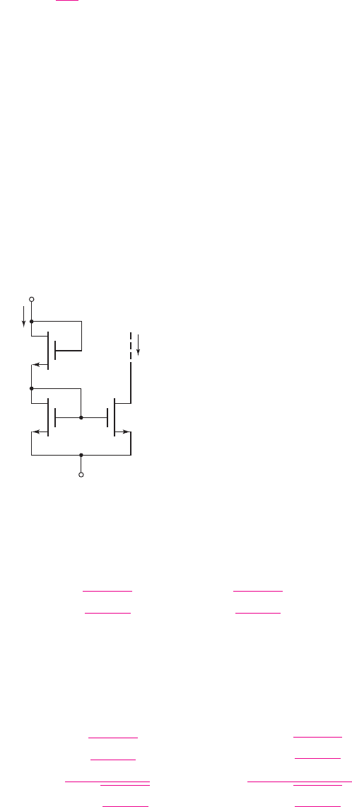
Consider the current mirror shown in Figure 10.17. Transistors M
1
and M
3
are in
series; assuming
λ = 0
, we can write,
K
n1
(V
GS1
− V
TN1
)
2
= K
n3
(V
GS3
− V
TN3
)
2
(10.49)
I
D2
= I
O
I
REF
V
–
V
+
++
––
V
GS1
+
–
V
GS3
V
GS2
M
1
M
3
M
2
Figure 10.17 MOSFET current source
If we again assume that
V
TN
, μ
n
, and C
ox
are identical in all transistors, then Equa-
tion (10.49) can be rewritten
V
GS1
=
(W/L)
3
(W/L)
1
· V
GS3
+
1 −
(W/L)
3
(W/L)
1
· V
TN
(10.50)
where
V
TN
is the threshold voltage of both transistors.
From the circuit, we see that
V
GS1
+ V
GS3
= V
+
− V
−
(10.51)
Therefore,
V
GS1
=
(W/L)
3
(W/L)
1
1 +
(W/L)
3
(W/L)
1
· (V
+
− V
−
) +
1 −
(W/L)
3
(W/L)
1
1 +
(W/L)
3
(W/L)
1
· V
TN
= V
GS2
(10.52)
nea80644_ch10_687-752.qxd 6/19/09 4:27 AM Page 709 pmath DATA-DISK:Desktop Folder:18.6.09:MHDQ134-10:

710 Part 2 Analog Electronics
Finally, the load current, for
λ = 0
, is given by
I
O
=
k
n
2
·
W
L
2
(V
GS2
− V
TN
)
2
(10.53)
Since the designer has control over the width-to-length ratios of the transistors,
there is considerable flexibility in the design of MOSFET current sources.
DESIGN EXAMPLE 10.8
Objective: Design a MOSFET current source circuit to meet a set of specifications.
Specifications: The circuit to be designed has the configuration shown in Fig-
ure 10.17. The bias voltages are
V
+
= 2.5
V and
V
−
= 0
. Transistors are available
with parameters
k
n
= 100 μ
A/V
2
,
V
TN
= 0.4
V, and
λ = 0
. Design the circuit such
that
I
REF
= 100 μ
A,
I
O
= 60 μ
A, and
V
DS2
(
sat
)
= 0.4
V.
Solution: We have
V
DS2
(
sat
)
= 0.4 = V
GS2
−0.4
, so that
V
GS2
= V
GS1
= 0.8
V.
Then for transistor
M
2
,
W
L
2
=
I
0
k
n
2
(V
GS2
− V
TN
)
2
=
60
100
2
(0.8 − 0.4)
2
= 7.5
For transistor
M
1
,
W
L
1
=
I
REF
k
n
2
(V
GS1
− V
TN
)
2
=
100
100
2
(0.8 − 0.4)
2
= 12.5
The value of
V
GS3
is found as
V
GS3
=
V
+
− V
−
− V
GS1
= 2.5 −0.8 = 1.7V
Then for transistor
M
3
we find
W
L
3
=
I
REF
k
n
2
(V
GS3
− V
TN
)
2
=
100
100
2
(1.7 − 0.4)
2
= 1.18
Trade-offs: As with other designs, slight variations in transistor parameters (
k
n
,
W/L
, and
V
TN
)
will change the current values slightly. See Test Your Understanding
exercise TYU 10.5.
Comment: In this design, the output transistor remains biased in the saturation
region for
V
DS
> V
DS
(sat) = V
GS
− V
TN
= 0.8 −0.4 = 0.4V
Design Pointer: As with most design problems, there is not a unique solution.
The general design criterion was that M
2
was biased in the saturation region over a
wide range of
V
DS2
values. Letting
V
GS2
= 0.8
V was somewhat arbitrary. If
V
GS2
were smaller, the width-to-length ratios of M
1
and M
2
would need to be larger. Larger
values of
V
GS2
would result in smaller width-to-length ratios.
The value of
V
GS3
is the difference between the bias voltage and V
GS1
. If V
GS3
becomes too large, the ratio (W/L)
3
will become unreasonably small (much less
than 1). Two or more transistors in series can be used in place of M
3
to divide the
voltage in order to provide reasonable W/L ratios (see end-of-chapter problems).
nea80644_ch10_687-752.qxd 6/19/09 4:27 AM Page 710 pmath DATA-DISK:Desktop Folder:18.6.09:MHDQ134-10:
Chapter 10 Integrated Circuit Biasing and Active Loads 711
EXERCISE PROBLEM
Ex 10.8: For the circuit shown in Figure 10.17, the bias voltages are
V
+
= 1.8
V and
V
−
=−1.8
V, and the transistor parameters are
V
TN
= 0.4
V,
k
n
= 100 μ
A/V
2
,
and
λ = 0
. Design the circuit such that
I
REF
= 0.5
mA and
I
O
= 0.1
mA, and that
M
2
remains biased in the saturation region for
V
DS2
≥ 0.4
V. (Ans.
(
W/L
)
1
= 62.5
,
(
W/L
)
2
= 12.5
,
(
W/L
)
3
= 1.74)
Problem-Solving Technique: MOSFET Current-Source Circuit
1. Analyze the reference side of the circuit to determine gate-to-source voltages.
Using these gate-to-source voltages, determine the bias current in terms of
the reference current.
2. To find the output resistance of the current source circuit, place a test voltage
at the output node and analyze the small-signal equivalent circuit. Keep in
mind that the reference current is a constant, which may make some of the
gate voltages constant or at ac ground.
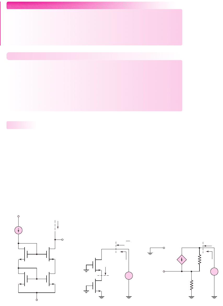
Multi-MOSFET Current-Source Circuits
Cascode Current Mirror
In MOSFET current-source circuits, the output resistance is a measure of the stability
with respect to changes in the output voltage. This output resistance can be increased
by modifying the circuit, as shown in Figure 10.18, which is a cascode current
mirror. The reference current is established by including another MOSFET in the
reference branch of the circuit as was done in the basic two-transistor current mirror.
Assuming all transistors are identical, then
I
O
= I
REF
.
To determine the output resistance at the drain of M
4
, we use the small-signal
equivalent circuit. Since I
REF
is a constant, the gate voltages to M
1
and M
3
, and
hence to M
2
and M
4
, are constant. This is equivalent to an ac short circuit. The ac
equivalent circuit for calculating the output resistance is shown in Figure 10.19(a).
10.2.2
I
REF
V
–
V
+
M
1
M
3
M
2
I
O
V
D4
M
4
Figure 10.18 MOSFET cascode
current mirror
(a)
r
o2
V
x
I
x
R
o
=
V
x
I
x
M
4
M
2
+
–
(b)
g
m
V
gs4
r
o4
r
o2
R
o
+
–
V
gs4
G
4
S
4
V
x
I
x
+
–
Figure 10.19 Equivalent circuits of the MOSFET cascode current mirror
for determining output resistance
nea80644_ch10_687-752.qxd 6/19/09 4:27 AM Page 711 pmath DATA-DISK:Desktop Folder:18.6.09:MHDQ134-10:

712 Part 2 Analog Electronics
The small-signal equivalent circuit is given in Figure 10.19(b). The small-signal
resistance looking into the drain of M
2
is r
O2
.
Writing a KCL equation, in phasor form, at the output node, we have
I
x
= g
m
V
gs4
+
V
x
−(−V
gs4
)
r
o4
(10.54)
Also,
V
gs4
=−I
x
r
o2
(10.55)
Substituting Equation (10.55) into (10.54), we obtain
I
x
+
r
o2
r
o4
I
x
+ g
m
r
o2
I
x
=
V
x
r
o4
(10.56)
The output resistance is then
R
o
=
V
x
I
x
= r
o4
+r
o2
(1 + g
m
r
o4
)
(10.57)
Normally,
g
m
r
o4
1
, which implies that the output resistance of this cascode
configuration is much larger than that of the basic two-transistor current source.
EXAMPLE 10.9
Objective: Compare the output resistance of the cascode MOSFET current source to
that of the two-transistor current source.
Consider the two-transistor current source in Figure 10.17 and the cascode
current source in Figure 10.18. Assume
I
REF
= I
O
= 100 μ
A in both circuits,
λ =
0.01 V
−1
for all transistors, and g
m
= 0.5 mA/V.
Solution: The output resistance of the two-transistor current source is, from Equa-
tion (10.48(b)),
r
o
=
1
λI
REF
=
1
(0.01)(0.10)
⇒ 1M
For the cascode circuit, we have
r
o2
= r
o4
= 1
M. Therefore, the output resistance
of the cascode circuit is, from Equation (10.57),
R
o
= r
o4
+r
o2
(1 + g
m
r
o4
) = 1 +(1)[1 +(0.5 × 10
−3
)(10
6
)]
or
R
o
= 502 M
Comment: The output resistance of the cascode current source is substantially
larger than that of the basic two-transistor circuit. Since
dI
O
∝ 1/R
o
, the load
current in the cascode circuit is more stable against variations in output voltage.
Design Pointer: Achieving the output resistance of 502 M assumes the transistors
are ideal. In fact, small leakage currents will begin to be a factor in actual output
resistance values, so a value of 502 M may not be achieved in reality.
nea80644_ch10_687-752.qxd 6/19/09 4:27 AM Page 712 pmath DATA-DISK:Desktop Folder:18.6.09:MHDQ134-10:
Chapter 10 Integrated Circuit Biasing and Active Loads 713
EXERCISE PROBLEM
Ex 10.9: In the MOSFET cascode current source shown in Figure 10.18, all
transistors are identical, with parameters:
V
TN
= 1
V,
K
n
= 80 μ
A/V
2
, and
λ =
0.02 V
−1
. Let
I
REF
= 20 μ
A. The circuit is biased at
V
+
= 5
V and
V
−
=−5
V.
Determine: (a) V
GS
of each transistor, (b) the lowest possible voltage value V
D4
, and
(c) the output resistance R
o
. (Ans. (a) V
GS
=
1.5 V (b)
V
D4
(min) =−3.0
V (c) R
o
=
505 M)
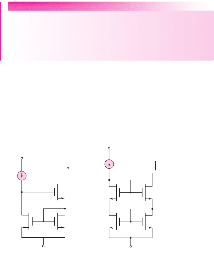
Wilson Current Mirror
Two additional multi-MOSFET current sources are shown in Figures 10.20(a) and
10.20(b). The circuit in Figure 10.20(a) is the Wilson current source. Note that the
V
DS
values of M
1
and M
2
are not equal. Since
λ
is not zero, the ratio I
O
/I
REF
is slightly
different from the aspect ratios. This problem is solved in the modified Wilson
current source, shown in Figure 10.20(b), which includes transistor M
4
. For a con-
stant reference current, the drain-to-source voltages of M
1
, M
2
, and M
4
are held
constant. The primary advantage of these circuits is the increase in output resistance,
which further stabilizes the load current.
(a) (b)
I
REF
V
–
V
+
M
1
M
2
I
O
M
3
I
REF
V
–
V
+
M
1
M
4
M
2
I
O
M
3
Figure 10.20 (a) MOSFET Wilson current source and (b) modified MOSFET Wilson current
source
Wide-Swing Current Mirror
If we consider the cascode current mirror in Figure 10.18, we can determine the min-
imum value of V
D4
, which will influence the maximum symmetrical swing of the
voltage in the load circuit being biased. The gate voltage of M
4
is
V
G4
= V
−
+ V
GS1
+ V
GS3
(10.58)
The minimum V
D4
is then
V
D4
(min) = V
G4
− V
GS4
+ V
DS4
(sat)
(10.59)
Assuming matched transistors,
V
GS1
= V
GS2
= V
GS4
≡ V
GS
. We then find
V
D4
(min) = V
−
+
(
V
GS
+ V
DS4
(sat)
)
(10.60)
nea80644_ch10_687-752.qxd 6/19/09 4:27 AM Page 713 pmath DATA-DISK:Desktop Folder:18.6.09:MHDQ134-10:
714 Part 2 Analog Electronics
In considering the simple two-transistor current mirror, the minimum output volt-
age is
V
O
(min) = V
−
+ V
DS
(sat)
(10.61)
If, for example,
V
GS
= 0.75
V and
V
TN
= 0.50
V, then from Equation (10.60),
V
D4
(min) = 1.0
V above
V
−
, and from Equation (10.61), V
O
(min) is only 0.25 V
above
V
−
. For bias voltages in the range of
±3.5
V, this additional required voltage
across the output of the cascode current mirror can have a significant effect on the
output of the load circuit.
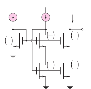
One current mirror circuit that does not limit the output voltage swing as
severely as the cascode circuit, but retains the high output resistance, is shown in Fig-
ure 10.21. Width-to-length ratios of the transistors are shown. Otherwise, the transis-
tors are assumed to be identical.
I
REF
V
Bias
M
5
M
4
M
1
V
D1
V
+
V
+
I
O
=
I
REF
M
3
M
2
I
REF
1
4
W
L
W
L
W
L
W
L
W
L
Figure 10.21 A wide-swing MOSFET cascode current mirror
The transistor pair M
3
and M
4
acts like a single diode-connected transistor in
creating the gate voltage for M
3
. By including M
4
, the drain-to-source voltage of M
3
is reduced and is matched to the drain-to-source voltage of M
2
. Since M
5
is one-
fourth the size of M
1
−M
4
and since all drain currents are equal, we have
(V
GS5
− V
TN
) = 2(V
GSi
− V
TN
)
(10.62)
where
V
GSi
corresponds to the gate-to-source voltage of M
1
−
M
4
.
The voltage at the gate of M
1
is
V
G1
= V
GS5
= (V
GS5
− V
TN
) + V
TN
(10.63)
The minimum output voltage at the drain of M
1
is
V
D1
(min) = V
G1
− V
GS1
+ V
DS1
(sat)
= [(V
GS5
− V
TN
) + V
TN
] − V
GS1
+(V
GS1
− V
TN
)
(10.64)
or
V
D1
(min) = V
GS5
− V
TN
= 2(V
GSi
− V
TN
) = 2V
DSi
(sat)
(10.65)
If we have
V
GSi
= 0.75
V and
V
TN
= 0.5
V, then V
D1
(min)
=
0.50 V, which is one-
half the value for the cascode circuit. At the same time, the high output resistance is
maintained.
nea80644_ch10_687-752.qxd 6/19/09 4:28 AM Page 714 pmath DATA-DISK:Desktop Folder:18.6.09:MHDQ134-10:
Chapter 10 Integrated Circuit Biasing and Active Loads 715
Discussion:
In the ideal circuit design in Figure 10.21, the transistors M
3
and M
4
are
biased exactly at the transition point between the saturation and non-saturation regions.
The analysis has neglected the body effect, so threshold voltages will not be exactly
equal. In an actual circuit design, therefore, the size of M
5
will be made slightly smaller
to ensure transistors are biased in the saturation region. This design change then means
that the minimum output voltage increases by perhaps 0.1 to 0.15 V.
Bias-Independent Current Source
In all of the current mirror circuits considered up to this point (both BJT and MOSFET),
the reference current is a function of the applied supply voltages. This implies that
the load current is also a function of the supply voltages. In most cases, the supply
voltage dependence is undesirable. Circuit designs exist in which the load currents
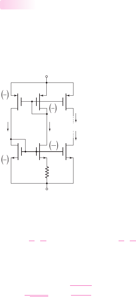
are essentially independent of the bias. One such MOSFET circuit is shown in Fig-
ure 10.22. The width-to-length ratios are given.
10.2.3
V
+
V
–
I
O2
I
D2
I
D1
I
O1
M
2
R
M
1
M
3
M
4
M
6
M
5
5
1
5
1
5
1
50
1
Figure 10.22 Bias-independent MOSFET current mirror
Since the PMOS devices are matched, the currents I
D1
and I
D2
must be equal.
Equating the currents in M
1
and M
2
, we find
I
D1
=
k
n
2
W
L
1
(V
GS1
− V
TN
)
2
= I
D2
=
k
n
2
W
L
2
(V
GS2
− V
TN
)
2
(10.66)
Also
V
GS2
= V
GS1
− I
D2
R
(10.67)
Substituting Equation (10.67) into Equation (10.66) and solving for R, we obtain
R =
1
√
K
n1
I
D1
1 −
(W/L)
1
(W/L)
2
(10.68)
This value of resistance R will establish the drain currents
I
D1
= I
D2
. These currents
establish the gate-to-source voltage across M
1
and source-to-gate voltage across M
3
.
nea80644_ch10_687-752.qxd 6/19/09 4:28 AM Page 715 pmath DATA-DISK:Desktop Folder:18.6.09:MHDQ134-10:
716 Part 2 Analog Electronics
These voltages, in turn, can be applied to M
5
and M
6
to establish load currents I
O1
and I
O2
.
The currents I
D1
and I
D2
are independent of the supply voltages
V
+
and
V
−
as
long as M
2
and M
3
are biased in the saturation region. As the difference,
V
+
− V
−
,
increases, the values of V
DS2
and V
SD3
increase but the currents remain essentially
constant.
Similar bipolar bias-independent current mirror designs exist, but will not be
covered here.
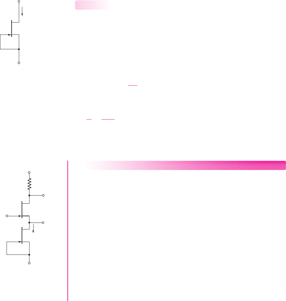
JFET Current Sources
Current sources are also fundamental elements in JFET integrated circuits. The simplest
method of forming a current source is to connect the gate and source terminals of a
depletion-mode JFET, as shown in Figure 10.23 for an n-channel device. The device
will remain biased in the saturation region as long as
v
DS
≥ v
DS
(sat) = v
GS
− V
P
=
|
V
P
|
(10.69)
In the saturation region, the current is
i
D
= I
DSS
1 −
v
GS
V
P
2
(1 + λv
DS
) = I
DSS
(1 + λv
DS
)
(10.70)
The output resistance looking into the drain is, from Equation (10.70),
1
r
o
=
di
D
dv
DS
= λI
DSS
(10.71)
This expression for the output resistance of a JFET current source is the same as
that of the MOSFET current source.
EXAMPLE 10.10
Objective: Determine the currents and voltages in a simple JFET circuit biased with
a constant-current source.
Consider the circuit shown in Figure 10.24. The transistor parameters are:
I
DSS1
= 2
mA,
I
DSS2
= 1
mA,
V
P1
= V
P2
=−1.5
V, and
λ
1
= λ
2
= 0.05 V
−1
.
Determine the minimum values of V
S
and V
I
such that Q
2
is biased in the saturation
region. What is the value of I
O
?
Solution: In order for Q
2
to remain biased in the saturation region, we must have
v
DS
≥
|
V
P
|
= 1.5V
, from Equation (10.69). The minimum value of V
S
is then
V
S
(min) − V
−
= v
DS
(min) = 1.5V
or
V
S
(min) = 1.5 + V
−
= 1.5 +(−5) =−3.5V
From Equation (10.70), the output current is
i
D
= I
O
= I
DSS2
(1 + λv
DS
) = (1)[1 +(0.05)(1.5)] = 1.08 mA
10.2.4
+
–
i
D
v
D
S
Figure 10.23 Depletion-
mode JFET connected
as a current source
Q
1
Q
2
I
O
V
S
V
I
V
O
V
+
= 5 V
V
–
= –5 V
R
D
Figure 10.24 The dc
equivalent circuit of simple
JFET amplifier biased
with JFET current source
nea80644_ch10_687-752.qxd 6/19/09 4:28 AM Page 716 pmath DATA-DISK:Desktop Folder:18.6.09:MHDQ134-10:

Chapter 10 Integrated Circuit Biasing and Active Loads 717
As a first approximation in calculating the minimum value of V
I
, we neglect the
effect of
λ
in transistor Q
1
. Then, assuming Q
1
is biased in the saturation region, we
have
i
D
= I
DSS1
1 −
v
GS1
V
P1
2
or
1.08 = 2
1 −
v
GS1
(−1.5)
2
which yields
v
GS1
=−0.40 V
We see that
v
GS1
=−0.40 V = V
I
− V
S
= V
I
−(−3.5)
or
V
I
=−3.90 V
Comment: Since Q
1
is an n-channel device, the voltage at the gate is negative with
respect to the source.
EXERCISE PROBLEM
*Ex 10.10: Consider the JFET circuit in Figure 10.24. The transistor parameters
are:
I
DSS2
= 0.5
mA,
I
DSS1
= 0.8
mA,
V
P1
= V
P2
=−2
V, and
λ
1
= λ
2
=
0.15 V
−1
. Determine the minimum values of V
S
and V
I
such that Q
2
is biased in
the saturation region. What is the value of I
O
? What is the output impedance look-
ing into the drain of Q
2
? (Ans.
V
S
(min) =−3
V,
I
O
= 0.65
mA,
V
I
(min) =
−3.2
V,
r
o
= 1.09
k
)
The output resistance of a JFET current source can be increased by using a cas-
code configuration. A simple JFET cascode current source with two n-channel
depletion-mode devices is shown in Figure 10.25. The current–voltage relationship,
assuming Q
1
and Q
2
are identical, is given by
i
D
= I
DSS
(1 + λv
DS1
) = I
DSS
1 −
v
GS2
V
P
2
(1 + λv
DS2
)
(10.72)
From the circuit, we see that
v
GS2
=−v
DS1
. We define
V
DS
= v
DS1
+v
DS2
(10.73(a))
so that
v
DS2
= V
DS
−v
DS1
(10.73(b))
From Equation (10.72), we obtain
(1 + λv
DS1
) =
1 +
v
DS1
V
P
2
[1 + λ(V
DS
−v
DS1
)]
(10.74)
For a given application, the value of
V
DS
will usually be known, and the value
of
v
DS1
can then be determined. The load current i
D
can then be calculated by using
Equation (10.72).
Q
1
Q
2
+
–
–
i
D
v
DS1
V
DS
++
–
v
DS2
Figure 10.25 JFET
cascode current source
nea80644_ch10_687-752.qxd 6/19/09 4:28 AM Page 717 pmath DATA-DISK:Desktop Folder:18.6.09:MHDQ134-10: