Neamen D. Microelectronics: Circuit Analysis and Design
Подождите немного. Документ загружается.


728 Part 2 Analog Electronics
The output voltage is
V
o
=−(g
m
V
π1
)(r
o
R
L
r
o2
)
(10.93)
Since
V
π1
= V
i
, where V
i
is the ac input voltage, the small-signal voltage gain is
A
v
=
V
o
V
i
=−g
m
(r
o
R
L
r
o2
) =
−g
m
1
r
o
+
1
R
L
+
1
r
o2
(10.94)
The small-signal voltage gain can also be written
A
v
=
−g
m
g
o
+ g
L
+ g
o2
(10.95)
where g
o
and g
o2
are the output conductances of Q
0
and Q
2
, and g
L
is the load con-
ductance. The transconductance is
g
m
= I
Co
/V
T
, the small-signal conductances are
g
o
= I
Co
/V
AN
and
g
o2
= I
Co
/V
AP
, and the load conductance is
g
L
= 1/R
L
. There-
fore, Equation (10.95) becomes
A
v
=
−
I
Co
V
T
I
Co
V
AN
+
1
R
L
+
I
Co
V
AP
(10.96)
If the passive load is an open circuit
(R
L
→∞)
, the small-signal voltage gain is
identical to that determined from the dc analysis as given by Equation (10.86). If the
load resistance R
L
is not an open circuit, then the magnitude of the small-signal volt-
age gain is reduced.
EXAMPLE 10.12
Objective: Calculate the small-signal voltage gain of an amplifier with an active
load and a load resistance R
L
.
For the circuit in Figure 10.37(a), the transistor parameters are
V
AN
= 120
V
and
V
AP
= 80
V. Let
V
T
= 0.026
V and
I
Co
= 0.2
mA. Determine the small-signal
voltage gain for load resistances of
R
L
=∞
, 200 k
, and 20 k
.
Solution: For
R
L
=∞
, Equation (10.96) reduces to
A
v
=
−
1
V
T
1
V
AN
+
1
V
AP
=
−
1
0.026
1
120
+
1
80
=−1846
which is the same as that determined for the open-circuit configuration in Exam-
ple 10.11.
For
R
L
= 200
k
, the small-signal voltage gain is
A
v
=
−
0.2
0.026
0.2
120
+
1
200
+
0.2
80
=
−7.692
0.001667 + 0.005 + 0.0025
=−839
nea80644_ch10_687-752.qxd 6/19/09 4:28 AM Page 728 pmath DATA-DISK:Desktop Folder:18.6.09:MHDQ134-10:
Chapter 10 Integrated Circuit Biasing and Active Loads 729
and for
R
L
= 20 k
, the voltage gain is
A
v
=
−
0.2
0.026
0.2
120
+
1
20
+
0.2
80
=
−7.692
0.001667 + 0.05 + 0.0025
=−142
Comment: The small-signal voltage gain is a strong function of the load resistance
R
L
. As the value of R
L
decreases, the loading effect becomes more severe.
Design Pointer: If an amplifier with an active load is to drive another amplifier
stage, the loading effect must be taken into account when the small-signal voltage
gain is determined. Also, the input resistance of the next stage must be large in order
to minimize the loading effect.
EXERCISE PROBLEM
Ex 10.12: For the circuit shown in Figure 10.37(a), the transistor parameters are
V
AN
= 100
V and
V
AP
= 60
V. Let
I
Co
= 0.25
mA. (a) Determine the open-circuit
small-signal voltage gain. (b) Find the value of
R
L
such that the voltage gain is
60 percent of the open-circuit value. (Ans. (a)
A
v
=−1442
, (b)
R
L
= 225
k
)
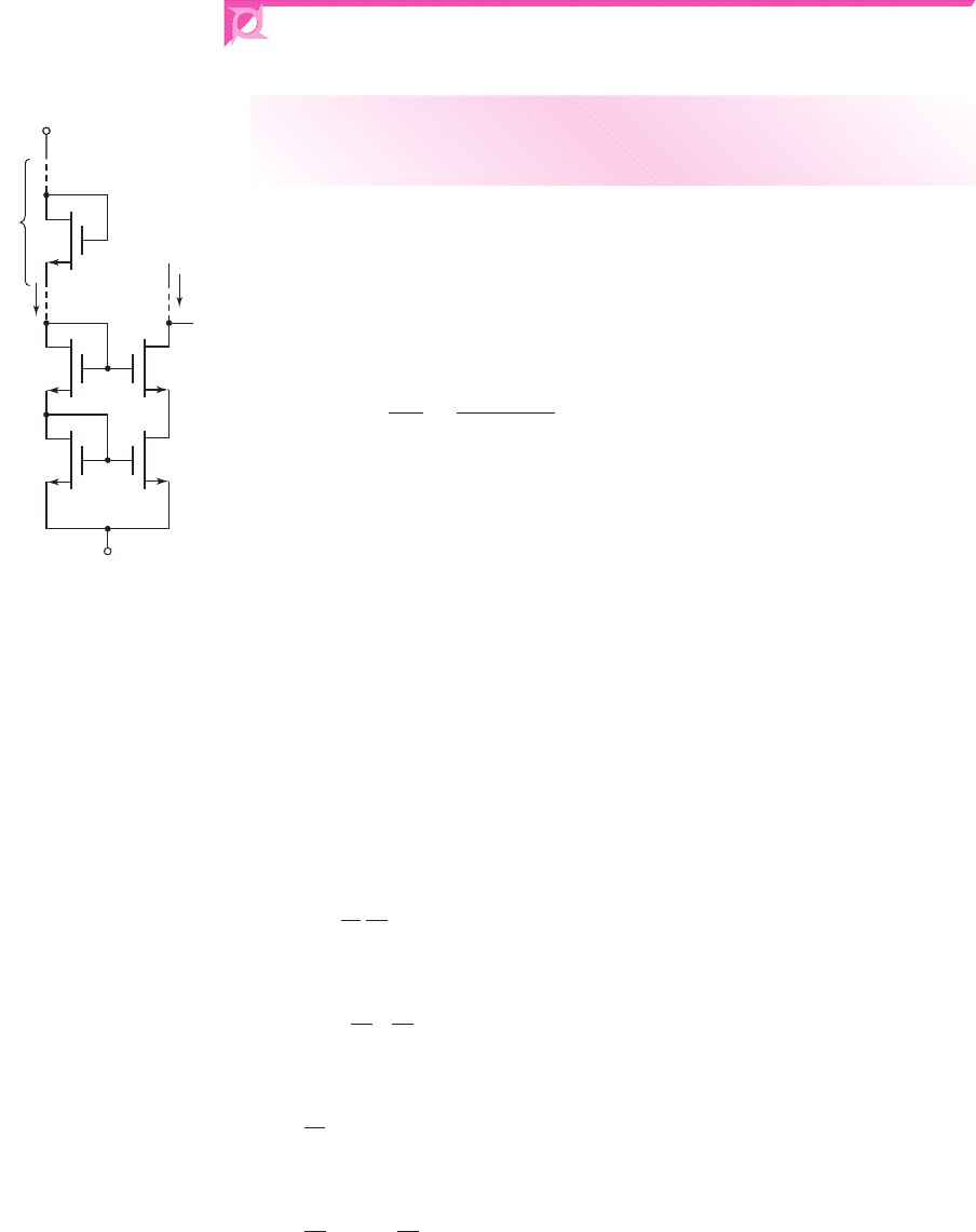
The small-signal voltage gain of an active-load circuit can be increased by in-
creasing the effective resistance of the active load. Figure 10.38 shows the same type
of BJT amplifier in which the active load is an “upside down” modified Widlar cur-
rent source. The small-signal voltage gain can be written in the same form as Equa-
tion (10.94), or
A
v
=
−g
m
1
r
o
+
1
R
L
+
1
R
o2
(10.97)
R
E2
R
o2
C
C
R
L
R
1
R
E1
Q
2
Q
1
Q
0
v
I
v
O
V
+
Figure 10.38 BJT amplifier with a modified Widlar current source as an active load
nea80644_ch10_687-752.qxd 6/19/09 4:28 AM Page 729 pmath DATA-DISK:Desktop Folder:18.6.09:MHDQ134-10:
730 Part 2 Analog Electronics
where R
o2
is now the effective resistance looking into the collector of Q
2
. We ana-
lyzed the output resistance of a Widlar current source in the Section 10.1. In this case,
however, we are including a resistor in the emitter of both transistors Q
1
and Q
2
. We
can show that
R
o2
= r
o2
1 + g
m2
R
E
(10.98a)
where
R
E
= R
E
[r
π2
+ R
1
(R
o1
+ R
E
)]
(10.98b)
and where
R
o1
= r
π1
1
g
m1
r
o1
(10.98c)
We may note that, if Q
1
and Q
2
are matched, then
g
m1
= g
m2
and
r
π1
= r
π2
since
the resistors in the emitters of Q
1
and Q
2
are the same value.
Problem-Solving Technique: Active Loads
1. Ensure that the active load devices are biased in the forward-active mode.
2. The small-signal analysis of the circuit with an active load then simply in-
volves considering the output resistance looking into the output of the active
load device as well as the equivalent circuit of the amplifying transistor.
Small-Signal Analysis: MOSFET Active Load Circuit
The small-signal voltage gain of a MOSFET amplifier with an active load can also be
determined from the small-signal equivalent circuit. Figure 10.39 is the small-signal
equivalent circuit of the entire MOSFET active load in Figure 10.33. The signal volt-
ages
V
sg1
and
V
sg2
are zero, since there is no ac excitation in this part of the circuit.
This means that
g
m
V
sg2
= 0
and
R
o
= r
o2
(10.99)
10.4.2
g
m
V
sg2
g
m
V
sg1
r
o1
r
o2
R
o
=
–
+
V
sg2
S
1
S
2
+
–
V
sg1
+
–
V
x
I
x
V
x
G
2
G
1
D
2
I
x
+
–
Figure 10.39 Small-signal equivalent circuit of the MOSFET active load circuit
A simple MOSFET amplifier with an active load, and a load resistor R
L
capaci-
tively coupled to the output, is shown in Figure 10.40(a). Figure 10.40(b) shows the
small-signal equivalent circuit, in which the load R
L
, the active load resistance r
o2
,
and the output resistance r
o
of transistor M
0
are included.
nea80644_ch10_687-752.qxd 6/19/09 4:28 AM Page 730 pmath DATA-DISK:Desktop Folder:18.6.09:MHDQ134-10:
Chapter 10 Integrated Circuit Biasing and Active Loads 731
(a) (b)
V
o
V
i
V
gs
g
m
V
gs
r
o2
r
o
+
+
–
–
R
L
V
+
v
I
v
O
I
REF
R
L
C
C
M
1
M
2
M
0
Figure 10.40 (a) Simple MOSFET amplifier with active load and load resistance and
(b) small-signal equivalent circuit
The output voltage is
V
o
=−g
m
V
gs
(r
o
R
L
r
o2
)
(10.100)
and since
V
gs
= V
i
, where V
i
is the ac voltage, the small-signal voltage gain is
A
v
=
V
o
V
i
=−g
m
(
r
o
R
L
r
o2
)
=
−g
m
g
o
+ g
L
+ g
o2
(10.101)
The parameters g
o
and g
o2
are the output conductances of M
0
and M
2
, and g
L
is the
load conductance. This expression for the small-signal voltage gain of a MOSFET
amplifier with active load is the same as that of the BJT amplifier.
A load resistance R
L
tends to degrade the gain and to cause a loading effect, as it
did in the bipolar circuit with an active load. However, in MOSFET amplifiers, the
output may be connected to the gate of another MOSFET amplifier in which the
effective R
L
is very large.
EXAMPLE 10.13
Objective: Calculate the small-signal voltage gain of an NMOS amplifier with an
active load.
For the amplifier shown in Figure 10.40(a) the transistor parameters are:
λ
n
= λ
p
= 0.01 V
−1
,
V
TN
= 1
V, and
K
n
= 1
mA/V
2
. Assume M
1
and M
2
are
matched and
I
REF
= 0.5
mA. Calculate the small-signal voltage gain for load resis-
tances of
R
L
=∞
and 100 k.
Solution: Since M
1
and M
2
are matched, then
I
O
= I
REF
, and the transconductance is
g
m
= 2
K
n
I
REF
= 2
(1)(0.5) = 1.41 mA/V
The small-signal transistor conductances are
g
o
= g
o2
= λI
REF
= (0.01)(0.5) = 0.005 mA/V
For
R
L
=∞
, Equation (10.101) reduces to
A
v
=
−g
m
g
o
+ g
o2
=
−1.41
0.005 + 0.005
=−141
nea80644_ch10_687-752.qxd 6/19/09 4:28 AM Page 731 pmath DATA-DISK:Desktop Folder:18.6.09:MHDQ134-10:
732 Part 2 Analog Electronics
For
R
L
= 100 k(g
L
= 0.01
mA/V), the voltage gain is
A
v
=
−g
m
g
o
+ g
L
+ g
o2
=
−1.41
0.005 + 0.01 +0.005
=−70.5
Comment: The magnitude of the small-signal voltage gain of MOSFET amplifiers
with active loads is substantially larger than for those with resistive loads, but it is
still smaller than equivalent bipolar circuits, because of the smaller transconductance
for the MOSFET.
EXERCISE PROBLEM
Ex 10.13: For the circuit in Figure 10.40(a), the transistor parameters are:
λ
n
=
λ
p
= 0.015 V
−1
,
K
n
= K
p
= 0.10
mA/V
2
,
V
TN
= 0.5
V, and
V
TP
=−0.5
V.
Let
V
+
= 5
V and
I
REF
= 0.20
mA. (a) Determine
V
IQ
. (b) Find the open-circuit
small-signal voltage gain. (c) Find the value of
R
L
that results in a voltage gain of
one-half the open-circuit value. (Ans. (a)
V
IQ
= 1.914
V, (b)
A
v
=−47.1
,
(c)
R
L
= 166
k
)
Small-Signal Analysis:
Advanced MOSFET Active Load
The active loads considered in the BJT (Figure 10.37) and MOSFET (Figure 10.40(a))
circuits correspond to the simple two-transistor current mirrors. We may use a more
advanced current mirror with a high output resistance as an active load to increase
the amplifier gain. Figure 10.41(a) shows a MOSFET cascode amplifying stage with
a cascode active load. The small-signal equivalent circuit is shown in Figure 10.41(b),
10.4.3
M
4
M
3
M
2
M
1
M
5
M
6
V
+
v
I
v
O
I
REF
V
Bias
R
o3
(a) (b)
G
2
D
2
S
1
D
1
G
1
R
o3
V
o
r
o2
r
o1
S
2
+
–
V
gs2
+
–
V
gs1
+
–
V
i
g
m1
V
gs1
g
m2
V
gs2
Figure 10.41 (a) MOSFET cascode amplifying stage with cascode active load; (b) small-
signal equivalent circuit
nea80644_ch10_687-752.qxd 6/19/09 4:28 AM Page 732 pmath DATA-DISK:Desktop Folder:18.6.09:MHDQ134-10:

Chapter 10 Integrated Circuit Biasing and Active Loads 733
where R
o3
is the effective resistance looking into the drain of M
3
. From our
discussion of the cascode current mirror, we found
R
o3
= r
o3
+r
o4
(1 + g
m
r
o3
)
(Equation (10.57)).
We can assume all transistors are matched so that the currents in all transistors
are equal. Summing currents at D
1
, we have
g
m
V
gs1
+
(−V
gs2
)
r
o1
= g
m
V
gs2
+
V
o
−(−V
gs2
)
r
o2
(10.102)
Summing currents at the output node, we find
V
o
R
o3
+
V
o
−(−V
gs2
)
r
o2
+ g
m
V
gs2
= 0
(10.103)
Eliminating
V
gs2
from the two equations, noting that
V
gs1
= V
i
, and assuming
g
m
1/r
o
, we find the small-signal voltage gain is
A
v
=
V
o
V
i
=
−g
2
m
g
m
R
o3
+
1
r
o1
r
o2
(10.104)
The resistance R
o3
is approximately
R
o3
∼
=
g
m
r
o3
r
o4
, so the gain can be written as
A
v
=
−g
2
m
1
r
o3
r
o4
+
1
r
o1
r
o2
(10.105)
For the same transistor parameters given in Example 10.13, the small-signal
voltage gain of this circuit would be 39,762! However, a word of warning is in order.
As we mentioned previously, output resistances in the hundreds of megohm range
are ideal and will, in reality, be limited by leakage currents. For this reason, a voltage
gain of 39,000 in a one-stage amplifier will probably not be achieved. However, the
voltage gain of this amplifier should be substantially larger than the amplifier using a
simple active load.
Test Your Understanding
TYU 10.12 In the circuit shown in Figure 10.37(a), the transistor parameters are
V
AN
= 120
V and
V
AP
= 80
V. Let
I
Co
= 0.5
mA and
R
L
= 50
k. (a) Determine
the small-signal parameters g
m
, r
o
, and r
o2
. (b) Find the small-signal voltage gain.
(Ans. (a)
g
m
= 19.2
mA/V,
r
o
= 240
k,
r
o2
= 160
k (b)
A
v
=−631
)
TYU 10.13 Repeat Example 10.12 for the case where a resistor
R
E
= 1
k is in-
cluded in the emitters of Q
1
and Q
2
as shown in Figure 10.38. (Ans. For
R
L
=∞
,
A
v
=−4404
; for
R
L
= 200
k
,
A
v
=−2800
; for
R
L
= 20
k
,
A
v
=−655
)
TYU 10.14 In the circuit in Figure 10.40(a), the transistor parameters are:
K
p
=
0.1 mA/V
2
,
K
n
= 0.2
mA/V
2
,
V
TN
= 1
V,
V
TP
=−1
V,
λ
n
= 0.01 V
−1
, and
λ
p
= 0.02 V
−1
. Let
V
+
= 10
V,
I
REF
= 0.25
mA, and
R
L
= 100
k. (a) Determine
the small-signal parameters
g
m
(for M
0
),
r
on
, and
r
op
. (b) Find the small-signal volt-
age gain. (Ans. (a)
g
m
= 0.448
mA/V,
r
on
= 400
k,
r
op
= 200
k (b)
A
v
=−25.6
)
nea80644_ch10_687-752.qxd 6/19/09 4:28 AM Page 733 pmath DATA-DISK:Desktop Folder:18.6.09:MHDQ134-10:
734 Part 2 Analog Electronics
10.5 DESIGN APPLICATION: AN NMOS
CURRENT SOURCE
Objective: • Design an NMOS current source circuit to provide a
specified bias current and output resistance.
Specifications: Design an NMOS current source to provide a bias current of
I
Q
= 100
μA and an output resistance greater than 20 M. The reference current is
to be
I
REF
= 150
μA. The circuit is to be biased at
±3.3
V and the voltage at the
drain of the current source transistor is to be no smaller than −2.2 V.
Design Approach: A simple two-transistor current source would yield an output
resistance of
R
o
= r
o
=
1
λI
Q
=
1
(0.01)(0.1)
⇒ 1M
Therefore, to obtain a larger output resistance, a cascode current source is required.
The basic circuit is shown in Figure 10.42. The transistor M
5
may actually need to be
two or more transistors in series.
Choices: NMOS transistors are available with the following parameters:
V
TN
=
0.5 V,
k
n
= 80 μA/V
2
, and
λ = 0.01 V
−1
. The minimum width-to-length ratio of
any transistor is to be unity.
Solution: The minimum voltage
V
D3
is to be
−2.2V
. This voltage is given by
V
D3
= V
GS1
+ V
DS3
(sat) + V
−
= V
GS1
+ V
GS3
− V
TN
+ V
−
Assuming that M
1
and M
3
are matched, we find
V
D3
=−2.2 = 2V
GS1
−0.5 +(−3.3)
or
V
GS1
= V
GS3
= 0.8V
Now
I
Q
=
k
n
2
W
L
(
V
GS1
− V
TN
)
2
or
100 =
80
2
W
L
1
(0.8 − 0.5)
2
which yields
W
L
1
= 27.8
If we set
W
L
1
=
W
L
3
= 28
then we find that
V
GS1
= V
GS3
= 0.799
V and
V
D3
(min) =−2.202
V.
M
5
M
4
I
REF
V
+
= 3.3 V
V
–
= –3.3 V
M
2
M
1
M
3
I
Q
V
D3
Figure 10.42 MOSFET
cascode current source circuit
for design application
nea80644_ch10_687-752.qxd 6/19/09 4:28 AM Page 734 pmath DATA-DISK:Desktop Folder:18.6.09:MHDQ134-10:
Chapter 10 Integrated Circuit Biasing and Active Loads 735
Assuming that M
2
and M
4
are matched, we have
I
REF
I
Q
=
(W/L)
2
(W/L)
1
or
150
100
=
(W/L)
2
28
which yields
W
L
2
=
W
L
4
= 42
Now the equivalent V
GS5
is given by
V
GS5
= V
+
−2V
GS2
− V
−
= 3.3 −2(0.799) −(−3.3)
or
V
GS5
= 5.0V
The width-to-length ratio is found from
I
REF
= 150 =
80
2
W
L
5
(5.0 − 0.5)
2
which yields
(W/L)
5
= 0.185
. A width-to-length ratio less than unity is unaccept-
able. Putting two equivalent M
5
transistors in series yields a gate-to-source voltage of
V
GS5
= 5.0/2
V. Then
I
REF
= 150 =
80
2
W
L
5
5.0
2
−0.5
2
which yields
(W/L)
5
= 0.938
. This value is still less than unity. Putting three equiv-
alent M
5
transistors in series yields a gate-to-source voltage of
V
GS5
= 5.0/3
V. Then
I
REF
= 150 =
80
2
W
L
5
5.0
3
−0.5
2
which yields
(W/L)
5
= 2.76
. This is an acceptable solution.
The output resistance is given by
R
o
= r
o3
+r
o1
(1 + g
m3
r
o3
)
We find
r
o1
= r
o3
=
1
λI
Q
=
1
(0.01)(0.1)
⇒ 1M
and
g
m3
= 2
k
n
2
W
L
3
I
Q
= 2
80
2
(28)(100) = 669 μA/V
We then find
R
o
= 1 +1
[
1 + (669)(1)
]
= 671 M
This value certainly meets the design criteria.
nea80644_ch10_687-752.qxd 6/19/09 4:28 AM Page 735 pmath DATA-DISK:Desktop Folder:18.6.09:MHDQ134-10:

736 Part 2 Analog Electronics
Comment: The very large output resistance of 671 M assumes that we have ideal
MOS transistors. In fact there are leakage currents that, in reality, will lower the out-
put resistance. However, the cascode current source does provide a very high output
resistance that is useful in differential amplifiers as we will see in Chapter 11.
10.6 SUMMARY
• This chapter addressed the biasing of bipolar and FET circuits with constant-
current sources. The current source biasing technique eliminates the need for
resistor-intensive biasing used up to this point.
• The basic bipolar current source is the simple two-transistor circuit with a resis-
tor to establish the reference current. The basic FET current source is also a sim-
ple two-transistor circuit but includes additional transistors in the reference
portion of the circuit. The relation between the bias current and reference current
was determined.
• One parameter of interest in the current source circuit is the output resistance,
which determines the stability of the bias current. More sophisticated current-
source circuits, such as the Widlar and Wilson circuits in the BJT configuration
and the Wilson and cascode circuits in the FET configuration, have larger output
resistance parameters and increased bias-current stability.
• Multitransistor output stages, in both bipolar and FET constant-current circuits,
are used to bias multiple amplifier stages with a single reference current. These
circuits, called current mirrors, reduce the number of elements required to bias
amplifier stages throughout an IC.
• Both bipolar and MOSFET active load circuits were analyzed. Active loads are
essentially “upside down” current-source circuits that replace the discrete col-
lector and drain resistors. The active loads produce a much larger small-signal
voltage gain compared to discrete resistor circuits.
• As an application, a MOSFET current source circuit was designed to provide a
specified bias current and output resistance.
CHECKPOINT
After studying this chapter, the reader should have the ability to:
✓ Analyze and design a simple two-transistor BJT current-source circuit to pro-
duce a given bias current.
✓ Analyze and design more sophisticated BJT current-source circuits, such as the
three-transistor circuit, cascode circuit, Wilson circuit, and Widlar circuit.
✓ Design a BJT current-source circuit to yield a specified output resistance.
✓ Analyze and design a basic two-transistor MOSFET current-source circuit with
additional MOSFET devices in the reference portion of the circuit to yield a
given bias current.
✓ Analyze and design more sophisticated MOSFET current-source circuits, such
as the cascode circuit, Wilson circuit, and wide-swing cascode circuit.
✓ Design a MOSFET current-source circuit to yield a specified output resistance.
✓ Describe the operation and characteristics of a BJT and MOSFET active load
circuit.
✓ Discuss the reason for the increased small-signal voltage gain when an active
load is used.
nea80644_ch10_687-752.qxd 6/19/09 3:55 PM Page 736 pmath DATA-DISK:Desktop Folder:19/6/2009:MHDQ134-10 Folder:MHDQ134-10
Chapter 10 Integrated Circuit Biasing and Active Loads 737
REVIEW QUESTIONS
1. Sketch the basic BJT two-transistor current source and explain the operation.
2. Explain the significance of the output resistance of the current-source circuit.
3. Discuss the effect of mismatched transistors on the characteristics of the BJT
two-transistor current source.
4. Sketch the BJT three-transistor current source and discuss the advantages of this
circuit.
5. What is the primary advantage of a BJT cascode current source?
6. Sketch a Widlar current source and explain the operation.
7. Can a piecewise linear model of the transistor be used in the analysis of the
Widlar current source? Why or why not?
8. Discuss the operation and significance of a multiple-output transistor current
mirror.
9. Sketch the basic MOSFET two-transistor current source and explain the operation.
10. Discuss the effect of mismatched transistors on the characteristics of the
MOSFET two-transistor current source.
11. Discuss how the reference portion of a MOSFET current source can be designed
with MOSFETs only.
12. Sketch a MOSFET cascode current source circuit and discuss the advantages of
this design.
13. Discuss the operation of an active load.
14. What is the primary advantage of using an active load?
15. Sketch the voltage transfer characteristics of a simple amplifier with an active
load. Where should the Q-point be placed?
16. What is the impedance seen looking into a simple active load?
17. What is the advantage of using a cascode active load?
PROBLEMS
Section 10.1 Bipolar Transistor Current Sources
10.1 Figure P10.1 shows another form of a bipolar current source. (a) Neglecting
base currents, derive the expression for I
C
in terms of the circuit, transistor,
and diode parameters. (b) If the transistor B–E and diode voltages are equal,
show that, for
R
1
= R
2
, the expression for I
C
reduces to
I
C
=
(−V
−
)
2R
3
(c) For
V
−
=−10
V and
V
BE
(on) = V
γ
= 0.7
V, design the circuit such
that
I
C
= I
1
= I
2
= 2
mA.
10.2 The matched transistors
Q
1
and
Q
2
in Figure 10.2(a) have parameters
I
S
= 10
−16
A. (a) For
β =∞
, determine
I
O
and
V
BE1
for (i)
I
REF
= 50 μ
A,
(ii)
I
REF
= 150 μ
A, and (iii)
I
REF
= 1.5
mA. (b) Repeat part (a) for
β = 50
.
10.3 Consider the circuit in Figure 10.2(a). Let
I
REF
= 200 μ
A. Assume transis-
tor parameters of
β = 80
,
I
S1
= 5 ×10
−15
A, and
I
S2
= 2 ×10
−15
A. Find
V
BE1
,
V
BE2
, and
I
O
.
10.4 Reconsider the circuit in Figure 10.2(a). Let
I
REF
= 150 μ
A. Assume tran-
sistor parameters of
β = 120
,
I
S1
= 10
−16
A, and
I
S2
= 3 ×10
−16
A. Find
V
BE1
,
V
BE2
, and
I
O
.
I
C
I
2
I
1
D
1
D
2
R
2
R
3
R
1
V
–
Q
Figure P10.1
nea80644_ch10_687-752.qxd 6/19/09 3:55 PM Page 737 pmath DATA-DISK:Desktop Folder:19/6/2009:MHDQ134-10 Folder:MHDQ134-10