Neamen D. Microelectronics: Circuit Analysis and Design
Подождите немного. Документ загружается.

718 Part 2 Analog Electronics
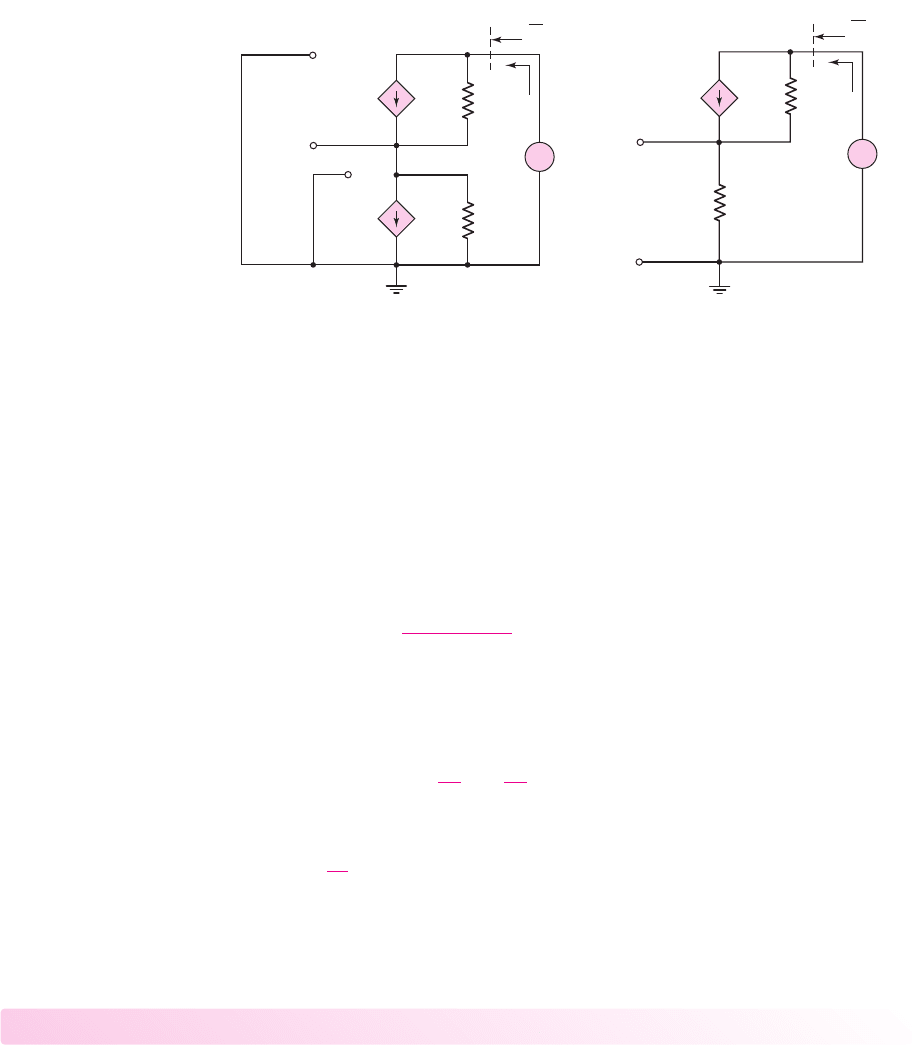
We can determine the output resistance by using the small-signal equivalent
circuit of the composite two-transistor configuration, as shown in Figure 10.26(a),
which includes the phasor variables. Since the gate and source of Q
1
are connected
together, the small-signal voltage V
gs1
is zero, which means that the dependent
current source g
m
V
gs1
is zero. This corresponds to an open circuit. Figure 10.26(b)
shows the final configuration.
The analysis is the same as for the MOSFET cascode circuit in Figure 10.19.
Writing a KCL equation at the output node, we have
I
x
= g
m
V
gs2
+
V
x
−(−V
gs2
)
r
o2
(10.75)
Noting that
V
gs2
=−I
x
r
o1
(10.76)
Equation (10.75) becomes
I
x
=−(g
m
r
o1
)I
x
+
V
x
r
o2
−
r
o1
r
o2
I
x
(10.77)
The output resistance is then
R
o
=
V
x
I
x
= r
o2
+r
o1
+ g
m
r
o1
r
o2
= r
o2
+r
o1
(1 + g
m
r
o2
)
(10.78)
From Equation (10.78), we see that the output resistance relationship for the
JFET cascode current source has the same form as that of the MOSFET cascode
current source.
Test Your Understanding
TYU 10.5 Consider Design Example 10.8. Assume transistor parameters of
k
n1
=
100 μ
A/V
2
,
k
n2
= 105 μ
A/V
2
,
k
n3
= 95 μ
A/V
2
,
V
TN1
= 0.38
V,
V
TN2
= 0.40
V,
V
TN3
= 0.42
V, and
λ
1
= λ
2
= λ
3
= 0
. (a) Using the designed values of
W/L
for
each transistor, determine the values of
I
REF
and
I
O
. (b) What is the percent change
in
I
REF
and
I
O
from Example 10.8? (Ans. (a)
I
REF
= 95.93 μ
A,
I
O
= 54.43 μ
A;
(b)
−4.06%
,
−9.28%)
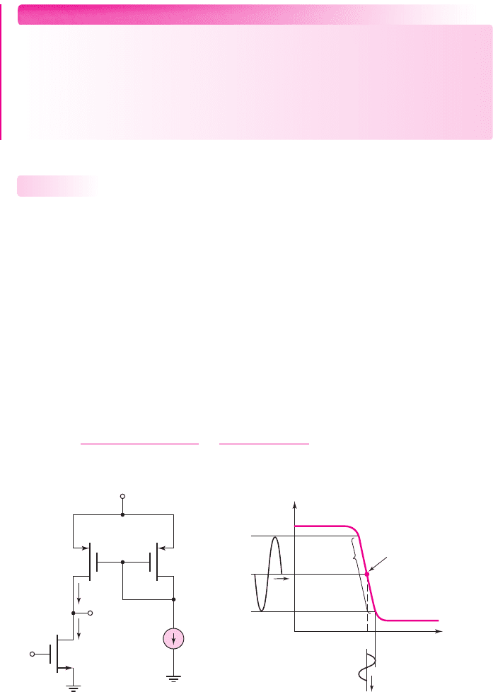
g
m
V
gs1
g
m
V
gs2
r
o2
r
o1
+
–
+
–
V
gs2
V
gs1
= 0
G
1
G
2
+
–
V
x
I
x
R
o
=
V
x
I
x
R
o
=
V
x
I
x
g
m
V
gs2
r
o2
r
o1
+
–
V
gs2
+
–
V
x
I
x
(a) (b)
+
–
+
–
Figure 10.26 (a) Equivalent circuit, using phasor notation, of the JFET cascode current
source for determining output resistance and (b) final configuration
nea80644_ch10_687-752.qxd 6/19/09 4:28 AM Page 718 pmath DATA-DISK:Desktop Folder:18.6.09:MHDQ134-10:
Chapter 10 Integrated Circuit Biasing and Active Loads 719
TYU 10.6 The bias voltages of the MOSFET current source in Figure 10.17 are
V
+
= 3
V and
V
−
=−3
V. The transistor parameters are
V
TN
= 0.5
V,
k
n
=
80 μ
A/V
2
, and
λ = 0.02
V
−1
. The transistor width-to-length ratios are
(
W/L
)
3
= 3
,
(
W/L
)
1
= 12
, and
(
W/L
)
2
= 6
. Determine: (a)
I
REF
, (b)
I
O
at
V
DS2
= 2
V, and (c)
I
O
at
V
DS2
= 4
V. (Ans. (a)
I
REF
= 1.33
mA, (b)
I
O
= 0.6936
mA, (c)
I
O
=0.7203
mA)
TYU 10.7 Consider the circuit shown in Figure 10.27. The bias voltages are changed
to
V
+
= 3
V and
V
−
=−3
V. The transistor parameters are
V
TN
= 0.7
V,
K
n1
= 0.35
mA/V
2
,
K
n2
= 0.30
mA/V
2
,
K
n3
= 0.10
mA/V
2
, and
λ = 0
. Determine
I
REF
and
I
O
. (Note: All transistors labeled
M
2
are identical.) (Ans.
I
REF
=
0.8986
mA,
I
O
= 2.31
mA)
I
O
I
REF
V
+
= 5 V
V
–
= –5 V
M
2
M
2
M
3
M
1
M
2
Figure 10.27 Figure for Exercise TYU 10.7
TYU 10.8
All transistors in the MOSFET modified Wilson current source in Figure
10.20(b) are identical. The parameters are:
V
TN
= 1
V,
K
n
= 0.2
mA/V
2
, and
λ = 0
.
If
I
REF
= 250 μ
A, determine I
O
and V
GS
for each transistor. (Ans.
I
O
= I
REF
=
250 μ
A,
V
GS
= 2.12
V)
10.3 CIRCUITS WITH ACTIVE LOADS
Objective: • Analyze the dc characteristics of amplifier circuits using
transistors as load devices (active loads).
In bipolar amplifiers, such as that shown in Figure 10.28, the small-signal voltage
gain is directly proportional to the collector resistor R
C
. To increase the gain, we need
to increase the value of R
C
, but there is a practical limitation. We can show that the
voltage gain (assuming C
C
acts as a short circuit to the signal frequency) of this
circuit is given by
A
v
=−g
m
R
C
where
g
m
=
I
CQ
V
T
V
CC
v
i
v
o
R
1
R
C
R
2
C
c
+
–
+
–
Figure 10.28 Bipolar
common-emitter circuit
nea80644_ch10_687-752.qxd 6/19/09 4:28 AM Page 719 pmath DATA-DISK:Desktop Folder:18.6.09:MHDQ134-10:
720 Part 2 Analog Electronics
Assuming the Q-point is in the center of the load line, then
I
CQ
=
V
CC
2R
C
or
R
C
=
V
CC
2I
CQ
Substituting into the voltage gain expression, we have
|
A
v
|
=
V
CC
2V
T
So for reasonable values of bias voltage, the maximum value of small-signal voltage
gain is essentially fixed.
To get around this limitation, we need a load device that will pass a given current
at a given bias voltage, but which will incrementally resist a change in current better
than the fixed R
C
. This load device can be a transistor, which will also occupy less
area in an integrated circuit, another advantage of using transistors in place of resis-
tors. In addition, active loads produce a much larger small-signal voltage gain than
discrete resistors, as discussed in Chapter 6.
In Chapter 4, we introduced NMOS enhancement load and depletion load
devices in MOSFET amplifiers. This was an introduction to active load devices. In
this section, we consider the dc analysis of a bipolar active load in a simple BJT
circuit and then the dc analysis of a MOSFET active load. Our discussion will
include the voltage gains of these active load circuits. The small-signal analysis of
active load circuits is covered in the next section.
The discussion of active loads here can be considered an introduction. The use
of active loads with differential amplifiers is considered in detail in the next chapter.
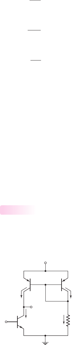
DC Analysis: BJT Active Load Circuit
Consider the circuit shown in Figure 10.29. The elements R
1
, Q
1
, and Q
2
form the
active load circuit, and Q
2
is referred to as the active load device for driver transis-
tor Q
0
. The combination of R
1
, Q
1
, and Q
2
forms the pnp version of the two-transistor
10.3.1
V
+
v
I
v
O
I
REF
R
1
Q
0
Q
1
Q
2
+
–
v
EC1
+
++
–
––
v
EC2
+
–
v
CE0
v
EB2
v
EB1
i
C1
i
C2
i
C0
Figure 10.29 Simple BJT amplifier with active load, showing currents and voltages
nea80644_ch10_687-752.qxd 6/19/09 4:28 AM Page 720 pmath DATA-DISK:Desktop Folder:18.6.09:MHDQ134-10:
Chapter 10 Integrated Circuit Biasing and Active Loads 721
current mirror. For the dc analysis of this circuit, we will use the dc symbols for the
currents and voltages. The objective of this analysis is to obtain the voltage transfer
function V
O
versus V
I
.
The B–E voltage of Q
0
is the dc input voltage V
I
; therefore, the collector current
in Q
0
is
I
C0
= I
S0
[e
V
I
/V
T
]
1 +
V
CE0
V
AN
(10.79)
where
I
S0
is the reverse-saturation current, V
T
is the thermal voltage, and
V
AN
is the
Early voltage of the npn transistor. Similarly, the collector current in Q
2
is
I
C2
= I
S2
[e
V
EB2
/V
T
]
1 +
V
EC2
V
AP
(10.80)
where
V
AP
is the Early voltage of the pnp transistors.
If we neglect base currents, then
I
REF
= I
C1
= I
S1
[e
V
EB1
/V
T
]
1 +
V
EC1
V
AP
(10.81)
Assuming Q
1
and Q
2
are identical, then
I
S1
= I
S2
and the Early voltages of
the pnp transistors are equal. Also note that
V
EC1
= V
EB1
= V
EB2
. We can also as-
sume that
V
CE
V
AN
and
V
EC
V
AP
. Combining equations, we find the output
voltage is given as
V
O
=
V
AN
V
AP
V
AN
+ V
AP
1 −
I
S0
e
V
I
/V
T
I
REF
+
V
AN
V
AN
+ V
AP
(V
+
− V
EB2
)
(10.82)
Equation (10.82) is valid as long as Q
0
and Q
2
remain biased in the forward-active
region, which means that the output voltage must remain in the range
V
CE0
(sat)<V
O
<(V
+
− V
EC2
(sat))
(10.83)
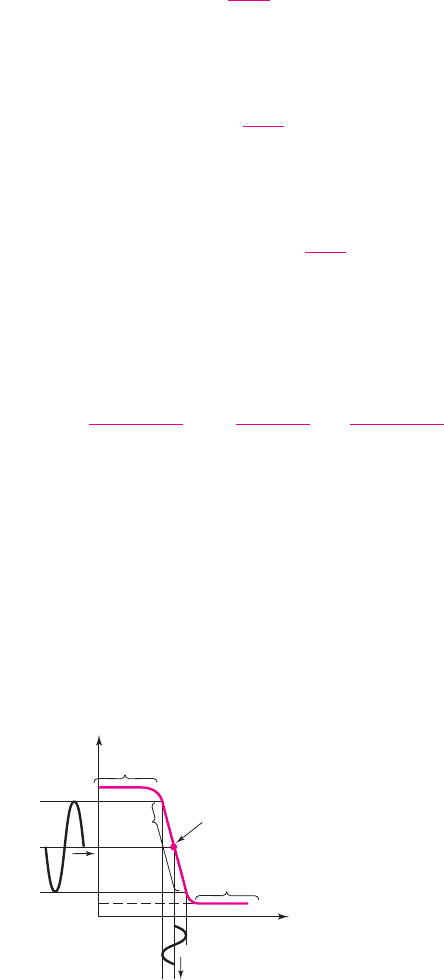
A sketch of V
O
versus V
I
is shown in Figure 10.30. If the circuit is to be used as
a small-signal amplifier, a Q-point must be established, as indicated in the figure, for
maximum symmetrical swing. Because of the exponential input voltage function, as
given in Equation (10.82), the input voltage range over which both Q
0
and Q
2
remain
in their active regions is very small. A sinusoidal variation in the input voltage
produces a sinusoidal variation in the output voltage as shown in the figure.
Q-point
Q
0
and
Q
2
active
Q
0
in saturation
Q
2
in saturation
v
O
V
CE0
(sat)
v
I
t
t
V
+
– V
EC2
(sat)
Figure 10.30 Voltage transfer characteristics
of bipolar circuit with active load
nea80644_ch10_687-752.qxd 6/19/09 4:28 AM Page 721 pmath DATA-DISK:Desktop Folder:18.6.09:MHDQ134-10:
722 Part 2 Analog Electronics
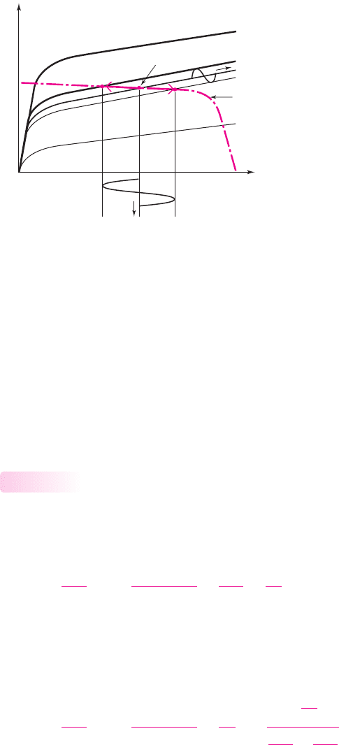
In addition to the voltage transfer function, we can also consider the load curve.
Figure 10.31 shows the transistor characteristics of the driver transistor Q
0
for sev-
eral values of B–E or V
I
voltages. Superimposed on these curves is the load curve,
which essentially is the I
C
versus
V
EC
characteristic of the active load Q
2
at a con-
stant
V
EB
voltage.
The Q-point shown corresponds to a quiescent input voltage
V
IQ
. From the
curve, we see that as the input changes between
V
IH
and
V
IL
, the Q-point moves up
and down the load curve producing a change in output voltage. Also, as V
I
increases
to
V
I2
, the driver transistor Q
0
is driven into saturation; as V
I
decreases to
V
I1
, the
load transistor Q
2
is driven into saturation.
Voltage Gain: BJT Active Load Circuit
The small-signal voltage gain of a circuit is the slope of the voltage transfer function
curve at the Q-point. For the bipolar circuit with an active load, the voltage gain can
be found by taking the derivative of Equation (10.82) with respect to V
I
, as follows:
A
v
=
dV
O
dV
I
=−
V
AN
V
AP
V
AN
+ V
AP
I
S0
I
REF
1
V
T
e
V
I
/V
T
(10.84)
As a good approximation, we can write that
I
REF
∼
=
I
S0
e
V
I
/V
T
(10.85)
Equation (10.84) then becomes
A
v
=
dV
O
dV
I
=−
V
AN
V
AP
V
AN
+ V
AP
1
V
T
=
−
1
V
T
1
V
AN
+
1
V
AP
(10.86)
The small-signal voltage gain is a function of the Early voltages and the thermal
voltage. The voltage gain, given by Equation (10.86), relates to the open-circuit
condition. When a load is connected to the output, the voltage gain is degraded, as we
will see in the next section.
10.3.2
I
C0
V
CE0
V
I1
V
IL
V
IQ
V
IH
V
I2
Load curve
Q-point
t
t
Figure 10.31 Driver transistor characteristics and load
curve for BJT circuit with active load
nea80644_ch10_687-752.qxd 6/19/09 4:28 AM Page 722 pmath DATA-DISK:Desktop Folder:18.6.09:MHDQ134-10:
Chapter 10 Integrated Circuit Biasing and Active Loads 723
EXAMPLE 10.11
Objective: Calculate the open-circuit voltage gain of a simple BJT amplifier with an
active load.
Consider the circuit shown in Figure 10.29. The transistor parameters are
V
AN
= 120
V and
V
AP
= 80
V. Let
V
T
= 0.026
V.
Solution: From Equation (10.86), the small-signal, open-circuit voltage gain is
A
v
=
−
1
V
T
1
V
AN
+
1
V
AP
=
−
1
0.026
1
120
+
1
80
=
−38.46
0.00833 + 0.0125
=−1846
Comment: For a circuit with an active load, the magnitude of the small-signal,
open-circuit voltage gain is substantially larger than the resulting gain when a
discrete resistor load is used.
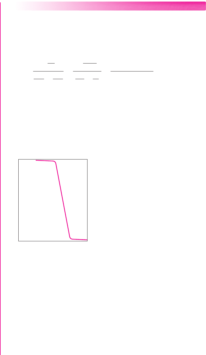
Computer Verification: The voltage transfer characteristics of the active load circuit
in Figure 10.29 were determined for a standard 2N3904 transistor as the npn device
and standard 2N3906 transistors as the pnp devices. The circuit was biased at 5 V and
the resistor was set at
R = 1k
. The transfer curve is shown in Figure 10.32.
720680
0
V
I
(mV)
V
O
(V)
5.0
Figure 10.32 Graphical output from a PSpice analysis, showing voltage transfer
characteristics of bipolar active load circuit
The input transition region, during which both Q
0
and Q
2
remain biased in the
forward-active mode, is indeed very narrow. The slope of the curve, which is the
voltage gain, is found to be
−572
. The reason for the smaller value compared to
the hand calculation is that the Early voltages of these standard transistors are smaller
than assumed in the previous calculation. The Early voltage of the npn device is 74 V
and that of the pnp devices is only 18.7 V.
Design Pointer: From the transfer characteristics in Figure 10.32, we can see that, for
this circuit, it would be very difficult to apply the required input voltage to bias both
Q
0
and Q
2
in the active region. This particular circuit, therefore, is not practical as an
amplifier. However, the circuit does demonstrate the basic properties of an active load.
In Chapters 11 and 13, we will see how an active load is applied to actual circuits.
nea80644_ch10_687-752.qxd 6/19/09 4:28 AM Page 723 pmath DATA-DISK:Desktop Folder:18.6.09:MHDQ134-10:
724 Part 2 Analog Electronics
EXERCISE PROBLEM
*Ex 10.11: A simple BJT amplifier with active load is shown in Figure 10.29. The
transistor parameters are:
I
S0
= I
S1
= I
S2
= 10
−12
A
and
V
AN
= V
AP
= 100 V
.
Let
V
+
= 5
V. (a) Determine the value of
V
EB2
such that
I
REF
= 0.5
mA. (b) Find
the value of R
1
. (c) What value of
V
I
will produce
V
CE0
= V
EC2
? (d) Determine
the open-circuit, small-signal voltage gain. (Ans. (a)
V
EB2
= 0.521
V (b)
R
1
=
8.96 k
(c)
V
I
= 0.521
V (d)
A
V
=−1923
)
DC Analysis: MOSFET Active Load Circuit
Consider the circuit in Figure 10.33. Transistors M
1
and M
2
form a PMOS active load
circuit, and M
2
is the active load device. We will consider the voltage transfer func-
tion of V
O
versus V
I
for this circuit.
The reference current may be written in the form
I
REF
= K
p1
(V
SG
+ V
TP1
)
2
(1 + λ
1
V
SD1
)
(10.87)
The drain current I
2
is
I
2
= K
p2
(
V
SG
+ V
TP2
)
2
(
1 + λ
2
V
SD2
)
(10.88)
If we assume that M
1
and M
2
are identical, then
λ
1
= λ
2
≡ λ
p
,
V
TP1
=
V
TP2
≡ V
TP
, and
K
p1
= K
p2
≡ K
p
. Combining equations, we find the output volt-
age as
V
O
=
[1 + λ
p
(V
+
− V
SG
)]
λ
n
+λ
p
−
K
n
(V
I
− V
TN
)
2
I
REF
(λ
n
+λ
p
)
(10.89)
10.3.3
V
+
V
I
V
O
I
REF
I
O
I
2
M
1
M
2
M
0
+
–
V
DS0
+
–
V
SD2
+
–
V
SD1
+
–
V
SG
Figure 10.33 Simple MOSFET
amplifier with active load, showing
currents and voltages
Q-point
M
0
and M
2
biased in
the saturation
region
V
O
V
IQ
V
I
t
t
Figure 10.34 Voltage transfer
characteristic of MOSFET circuit
with active load
Equation (10.89) describes that V
O
versus V
I
characteristic of the circuit, provided
that both M
0
and M
2
remain biased in their saturation regions. Figure 10.34 shows a
sketch of the voltage transfer characteristics. If the circuit is to be used as a small-signal
amplifier, then a Q-point must be established, as indicated on the figure, for maximum
symmetrical swing. As before, the input transition region in which both M
0
and M
2
are
nea80644_ch10_687-752.qxd 6/19/09 4:28 AM Page 724 pmath DATA-DISK:Desktop Folder:18.6.09:MHDQ134-10:
Chapter 10 Integrated Circuit Biasing and Active Loads 725
biased in the saturation region is quite narrow. A sinusoidal variation in the input voltage
produces a sinusoidal variation in the output voltage as shown in the figure.
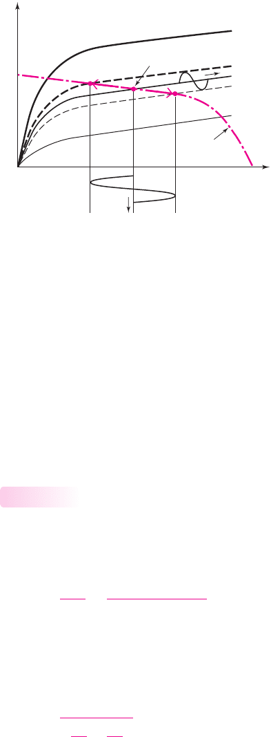
We can also consider the load curve for this device. Figure 10.35 shows the tran-
sistor characteristics of the driver transistor M
0
for several values of gate-to-source or
V
I
voltages. Superimposed on these curves is the load curve, which essentially is the
I
D
versus
V
SD
characteristic of the active load M
2
at a constant
V
SG
voltage.
The Q-point shown corresponds to a quiescent input voltage V
IQ
. From the
curve, we see that as the input changes between
V
IH
and
V
IL
, the Q-point moves up
and down the load curve producing a change in output voltage. Also, as V
I
increases
to
V
I2
, the driver transistor M
0
is driven into the nonsaturation region; as V
I
decreases
to
V
I1
, the load transistor M
2
is driven into the non-saturation region.
Voltage Gain: MOSFET Active Load Circuit
The small-signal voltage gain of a MOSFET circuit with an active load is also the
slope of the voltage transfer function curve at the Q-point. Taking the derivative of
Equation (10.89) with respect to V
I
, we obtain
A
v
=
dV
O
dV
I
=
−2K
n
(V
I
− V
TN
)
I
REF
(λ
n
+λ
p
)
(10.90)
The transconductance of the driver transistor is
g
m
= 2K
n
(V
I
− V
TN
)
. Since M
1
and M
2
are assumed to be identical, then
I
O
= I
REF
, and the small-signal transistor
resistances are
r
on
= 1/λ
n
I
REF
and
r
op
= 1/λ
p
I
REF
. From Equation (10.90), the
small-signal, open-circuit voltage gain can now be written
A
v
=
−g
m
1
r
on
+
1
r
op
=−g
m
(r
on
r
op
)
(10.91)
In general, the transconductance g
m
of a MOSFET is less than that of a BJT;
therefore, the voltage gain of a MOSFET amplifier with an active load is less than
that of a BJT amplifier with an active load. However, the active load still produces a
significant increase in the voltage gain.
10.3.4
I
D
V
DS0
V
I1
V
IL
V
IQ
V
IH
V
I2
Load curve
Q-point
t
t
Figure 10.35 Driver transistor characteristics and load curve for MOSFET circuit with
active load
nea80644_ch10_687-752.qxd 6/19/09 4:28 AM Page 725 pmath DATA-DISK:Desktop Folder:18.6.09:MHDQ134-10:

726 Part 2 Analog Electronics
Discussion
In considering the BJT circuit with active load (Figure 10.29) and MOSFET circuit
with active load (Figure 10.33), we could have directly considered the small-signal
analysis without the dc analysis. However, it is important to understand how nar-
row the input transition width is (Figure 10.32) such that the transistors are biased
correctly. For this reason, the use of active loads in discrete circuits is almost im-
possible. The biasing of the circuit with an active load depends to a large extent on
the use of matched transistors. Matched transistors can be achieved on an inte-
grated circuit. So in considering the small-signal analysis in the next section, we
must keep in mind the very narrow range in which the transistors are biased in the
active region.
Test Your Understanding
TYU 10.9 Repeat Exercise Problem 10.11 if the transistor parameters are
I
SO
=
I
S1
= I
S2
= 5 ×10
−14
A
and if
I
REF
= 0.1
mA. (Ans. (a)
V
EB2
= 0.557
V (b)
R
1
=
44.4k
(c)
V
I
= 0.557
V (d)
A
v
=−1923
)
TYU 10.10 Consider the simple MOSFET amplifier with active load in Figure 10.33.
The transistor parameters are
V
TN
= 0.7
V,
V
TP
=−0.7
V,
K
n
= K
p
= 0.12
mA/V
2
,
and
λ
n
= λ
p
= 0.02
V
−1
. Let
V
+
= 5
V and
I
REF
= 0.15
mA. (a) Determine
V
SG
.
(b) Find the value of
V
I
that produces
V
DSO
= V
SD2
. (c) Determine the open-
circuit small-signal voltage gain. (Ans. (a)
V
SG
= 1.818
V, (b)
V
I
= 1.798
V,
(c)
A
v
=−43.9)
TYU 10.11 Repeat Exercise TYU 10.10 if the transistor parameters are
K
n
=
K
p
= 50 μ
A/V
2
, and if
I
REF
= 80 μ
A. Other transistor parameters are as given in
TYU 10.10. (Ans. (a)
V
SG
= 1.965
V, (b)
V
I
= 1.940
V, (c)
A
v
=−38.74)
10.4 SMALL-SIGNAL ANALYSIS:
ACTIVE LOAD CIRCUITS
Objective: • Analyze the small-signal characteristics of amplifier
circuits with active loads.
The small-signal voltage gain of a circuit with an active load can be determined from
the small-signal equivalent circuit. This is probably the easiest and most direct
method of obtaining the gain of such circuits. Again, the dc analysis of these circuits,
as shown in the previous section, clearly demonstrates the narrow range of input
voltages over which the transistors will remain biased in the active region. The load
curves in Figure 10.31 for the BJT circuit and in Figure 10.35 for the MOSFET
circuit also help in visualizing the operation of these circuits. Even though a small-
signal analysis is extremely useful for determining the voltage gain, we must not lose
sight of the physical operation of these circuits, which is described through the dc
analysis. If the BJTs are not biased in the active region or the MOSFETs are not
biased in the saturation region, the small-signal analysis is not valid.
10.3.5
nea80644_ch10_687-752.qxd 6/19/09 4:28 AM Page 726 pmath DATA-DISK:Desktop Folder:18.6.09:MHDQ134-10:
Chapter 10 Integrated Circuit Biasing and Active Loads 727
Small-Signal Analysis: BJT Active Load Circuit
To find the small-signal voltage gain of the BJT circuit with an active load, we
must determine the resistance looking into the collector of the active load device.
Figure 10.36 is the small-signal equivalent circuit of the entire active load circuit in
Figure 10.29, which uses pnp transistors. The base, collector, and emitter terminals
of the two transistors are indicated on the figure.
10.4.1
+
–
r
p 1
g
m
V
p 2
g
m
V
p 1
r
o1
r
o2
R
o
=
+
–
V
p 2
E
1
B
1
C
1
B
2
C
2
E
2
+
–
V
p 1
r
p 2
V
x
I
x
V
x
R
1
I
x
Figure 10.36 Small-signal equivalent circuit of BJT active load circuit
(a) (b)
V
+
v
I
v
O
R
1
R
L
C
C
Q
2
Q
0
Q
1
r
p o
V
o
V
i
g
m
V
p1
r
o2
r
o
+
–
+
–
V
p1
R
L
Figure 10.37 (a) Simple BJT amplifier with active load and load resistance and (b) small-
signal equivalent circuit
In the Q
1
portion of the equivalent circuit, there are no independent ac sources to
excite any currents or voltages. Therefore,
V
π1
= V
π2
= 0
, which means that the de-
pendent source
g
m
V
π2
is zero and is equivalent to an open circuit. The resistance
looking into the collector of Q
2
is just
R
o
= r
o2
(10.92)
We will use this equivalent resistance to calculate the small-signal voltage gain of the
amplifier.
Figure 10.37(a) shows a simple amplifier with an active load and the output volt-
age capacitively coupled to passive load R
L
. The small-signal equivalent circuit,
shown in Figure 10.37(b), includes the load resistance R
L
, the resistance r
o2
of the
active load, and the output resistance r
o
of the amplifying transistor Q
0
.
nea80644_ch10_687-752.qxd 6/19/09 4:28 AM Page 727 pmath DATA-DISK:Desktop Folder:18.6.09:MHDQ134-10: