Neamen D. Microelectronics: Circuit Analysis and Design
Подождите немного. Документ загружается.

738 Part 2 Analog Electronics
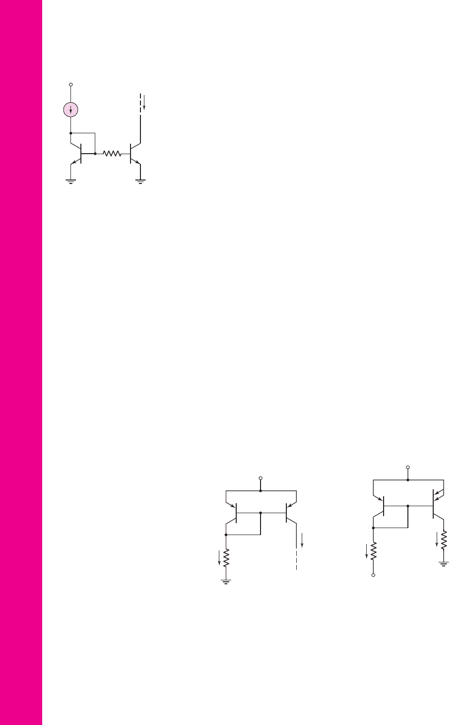
V
+
= 5 V
I
O
Q
2
Q
1
I
REF
R
1
+
–
V
EC2
Figure P10.11
V
+
= 5 V
V
–
= –5 V
I
O
Q
1
I
REF
R
1
R
C2
Q
2
Figure P10.13
I
O
I
REF
Q
2
Q
1
V
+
= 2.5 V
R
Figure P10.5
10.5 Consider the circuit shown in Figure P10.5. Assume
I
REF
= 200 μ
A and
R = 2
k
. The transistor parameters are
β = 40
,
I
S1
= I
S2
= 5 ×10
−15
A.
Find
V
BE1
,
V
BE2
, and
I
O
.
10.6 The transistor and circuit parameters for the circuit in Figure 10.2(b) are:
V
BE
(on) = 0.7
V,
β = 60
,
V
A
=∞
,
V
+
=+3
V,
V
−
=−3
V, and
I
REF
=
0.250
mA. Determine the value of R
1
and determine I
C1
, I
B1
, I
B2
, and
I
C2
.
10.7 The bias voltages in the circuit shown in Figure 10.2(b) are
V
+
=+5
V,
V
−
=−5
V and the resistor value is
R
1
= 18.3
k. Assume transistor pa-
rameters of
V
BE
(on) = 0.7 V,
β = 80
, and
V
A
=∞
. Determine I
REF
, I
C1
,
I
B1
, I
B2
, and I
C2
.
10.8 Consider the current source in Figure 10.2(b). The circuit is biased at
V
+
= 2.5
V and
V
−
=−2.5
V. The transistor parameters are
β
∼
=
∞
,
V
A
=∞
, and
I
S2
= 10
−15
A. The circuit is to be designed such that
I
O
= 0.25
mA and the power dissipated in the circuit is no greater than
1.8 mW. (a) Determine the maximum value of
I
REF
, (b) the required value
of
I
S1
, and (c) the required value of
R
1
.
10.9 For the basic two-transistor current source in Figure 10.2(b), the transistor
parameters are:
β = 120
,
V
BE
(
on
)
= 0.7
V, and
V
A
= 100
V. The bias volt-
ages are
V
+
= 5
V and
V
−
=−5
V. (a) Design the circuit such that
I
O
= 0.5
mA when
V
CE2
= 0.7
V. (b) What is the percent change in
I
O
as
V
CE2
varies between 0.7 V and 7 V?
10.10 The transistors in the basic current mirror in Figure 10.2(b) have a finite β
and an infinite Early voltage. The B–E area of
Q
2
is n times that of
Q
1
.
Derive the expression for
I
O
in terms of
I
REF
, β, and n.
D10.11 Figure P10.11 shows a basic two-transistor pnp current source. The trans-
istor parameters are V
EB
(on) = 0.7 V,
β = 40
, and
V
A
=∞
. Design the
circuit such that
I
O
= 0.20
mA and determine the value of I
REF
.
D10.12 In the circuit in Figure P10.11, the transistor parameters are
β = 80
and
V
EB
(
on
)
= 0.7
V. (a) Design the circuit such that
I
O
= 120 μ
A for
V
EC2
=
0.7
V. (b) If
V
A
= 80
V, determine the change in
I
O
for (i)
V
EC2
= 2
V and
(ii)
V
EC2
= 4
V.
D10.13 Consider the pnp current source in Figure P10.13, with transistor parame-
ters
β =∞
,
V
A
=∞
, and
V
EB
(on) = 0.7
V. (a) Design the circuit such
that I
REF
= 1 mA. (b) What is the value of I
O
? (c) What is the maximum
value of R
C2
such that
Q
2
remains biased in the forward-active mode?
nea80644_ch10_687-752.qxd 6/19/09 4:28 AM Page 738 pmath DATA-DISK:Desktop Folder:18.6.09:MHDQ134-10:
Chapter 10 Integrated Circuit Biasing and Active Loads 739
10.14 Consider the circuit shown in Figure P10.14. The transistor
Q
2
is equivalent
to two identical transistors in parallel, each of which is matched to
Q
1
. As-
sume the transistor parameters are V
BE
(on) = 0.7 V,
β = 60
, and
V
A
=∞
,
and assume the bias voltage is
V
+
= 2.5
V. Design the circuit such that
I
O
= 0.50
mA and determine the value of I
REF
.
D10.15 Design a basic two-transistor current source circuit configuration such
that
I
O
= 0.40
mA and I
REF
= 0.20 mA. The circuit is to be biased at
V
+
= 2.5
V and
V
−
=−2.5
V. Neglect base currents and assume that
V
BE
(
on
)
= 0.7
V and
V
A
=∞
.
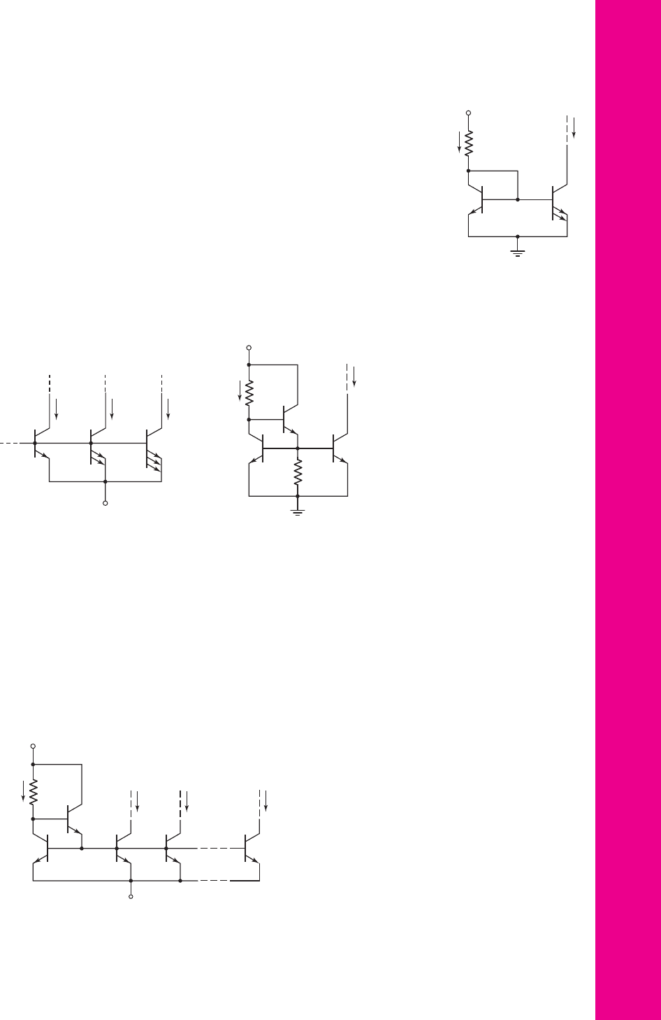
10.16 The values of β for the transistors in Figure P10.16 are very large. (a) If
Q
1
is diode-connected with
I
1
= 0.5
mA, determine the collector currents in
the other two transistors. (b) Repeat part (a) if
Q
2
is diode-connected with
I
2
= 0.5 mA. (c) Repeat part (a) if
Q
3
is diode-connected with I
3
= 0.5 mA.
I
O
I
REF
Q
1
R
1
V
+
Q
2
Figure P10.14
Q
1
Q
2
Q
3
V
–
I
1
I
2
I
3
Figure P10.16
I
O
I
REF
Q
1
Q
3
R
1
V
+
R
2
Q
2
Figure P10.17
10.17 Consider the circuit in Figure P10.17. The transistor parameters are:
β = 80
,
V
BE
(on) = 0.7 V, and
V
A
=∞
. (a) Derive the expression for I
O
in terms of
I
REF
, β, and R
2
. (b) For R
2
= 10 k and
V
+
= 10
V, design the circuit such
that
I
O
= 0.70
mA. What is the value of I
REF
?
10.18 All transistors in the N output current mirror in Figure P10.18 are matched,
with a finite β and
V
A
=∞
. (a) Derive the expression for each load current in
terms of I
REF
and β. (b) If the circuit parameters are
V
+
= 5
V and
V
−
=−5
V, and the transistor parameter is
β = 50
, determine R
1
such that each load
current is 0.5 mA for
N = 5
. Assume that
V
EB
(Q
R
) = V
BE
(Q
S
) = 0.7
V.
I
O1
I
REF
V
+
V
–
Q
R
Q
S
R
1
Q
1
Q
2
I
O2
I
ON
Q
N
Figure P10.18
nea80644_ch10_687-752.qxd 6/19/09 4:28 AM Page 739 pmath DATA-DISK:Desktop Folder:18.6.09:MHDQ134-10:
740 Part 2 Analog Electronics
D10.19 Design a pnp version of the basic three-transistor current source circuit,
using a resistor to establish
I
REF
. The bias current is to be
I
O
= 0.15
mA,
and the circuit is to be biased at
V
+
= 3
V and
V
−
=−3
V. The transistor
parameters are
β = 40
,
V
EB
(
on
)
= 0.7
V, and
V
A
=∞
.
D10.20 Design a pnp version of the Wilson current source, using a resistor to estab-
lish I
REF
. The circuit parameters are
V
+
= 9
V and
V
−
=−9V
, and the
transistor parameters are:
V
EB
(on) = 0.7 V,
β = 25
, and
V
A
=∞
. If the
load current is 0.8 mA, what is I
REF
?
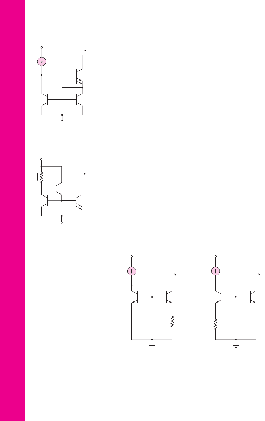
*10.21 Consider the Wilson current source in Figure P10.21. The transistors have a
finite β and an infinite Early voltage. Derive the expression for I
O
in terms
of I
REF
and
β
.
10.22 Consider the circuit in Figure P10.22. The transistor parameters for
Q
1
and
Q
2
are
V
BE1,2
(
on
)
= 0.7
Vand
β
1,2
= 90
. The parameters for
Q
3
are
V
BE3
(
on
)
= 0.6
V and
β
3
= 60
. Assume
V
A
=∞
for all transistors. Design
the circuit such that
I
O
= 0.5
mA. (a) What are the values of
I
REF
and
R
1
?
(b) What are the values of
I
B1
,
I
B2
,
I
E3
, and
I
B3
?
10.23 Consider the Wilson current-source circuit shown in Figure 10.8. Assume
the reference current is 0.25 mA and assume transistor parameters of
V
BE
(on) = 0.7 V,
β = 100
, and
V
A
= 100
V. (a) Determine the output re-
sistance looking into the collector of Q
3
. (b) What is the change in I
O
as the
output voltage changes by
+5
V?
10.24 Consider the Widlar current source shown in Figure 10.9. The circuit para-
meters are
V
+
=+5
V,
V
−
= 0
,
R
1
= 9.3
k, and
R
E
= 1.5
k. Assume
V
BE1
= 0.7
V. Neglecting base currents, determine I
REF
, I
O
, and
V
BE2
.
10.25 For the circuit shown in Figure P10.25, neglect base currents and assume
V
A
=∞
. Let
I
REF
= 200 μ
A and
R
E
= 500
. (a) Assume the transis-
tor parameters are
I
S1
= I
S2
= 5 ×10
−15
A. Find
V
BE1
,
V
BE2
, and
I
O
.
(b) Repeat part (a) if the transistor parameters are
I
S1
= 5 ×10
−15
A and
I
S2
= 7 ×10
−15
A.
I
O
I
REF
Q
1
V
–
Q
3
V
+
Q
2
Figure P10.21
I
O
I
REF
Q
1
Q
3
R
1
–5 V
+ 5 V
Q
2
Figure P10.22
V
+
I
O
Q
1
Q
2
R
E
I
REF
Figure P10.25
Figure P10.26
V
+
I
O
Q
1
Q
2
R
E
I
REF
10.26 Consider the circuit in Figure P10.26. Neglect base currents and assume
V
A
=∞
. Assume
I
REF
= 100 μ
A and
R
E
= 700
. (a) For transistor para-
meters of
I
S1
= I
S2
= 5 ×10
−15
A, find
V
BE1
,
V
BE2
, and
I
O
. (b) Repeat
nea80644_ch10_687-752.qxd 6/19/09 4:28 AM Page 740 pmath DATA-DISK:Desktop Folder:18.6.09:MHDQ134-10:

Chapter 10 Integrated Circuit Biasing and Active Loads 741
part (a) if the transistor parameters are
I
S1
= 5 ×10
−15
A and
I
S2
=
2 × 10
−15
A.
10.27 (a) For the Widlar current source shown in Figure 10.9, find
I
REF
,
I
O
, and
V
BE2
if
R
1
= 50
k
,
R
E
= 3
k
,
V
+
= 5
V, and
V
−
=−5
V. The transistor para-
meters are
β = 120
and
V
BE1
(
on
)
= 0.7
V. (b) Determine
R
o
for
V
A
= 80
V.
*10.28 Consider the Widlar current source in Problem 10.27. For
β = 80
and
V
A
= 80
V, determine the change in I
O
corresponding to a 5 V change in the
output voltage.
D10.29 (a) Design the Widlar current source such that I
REF
= 0.50 mA and I
O
=
50 μA. Assume that
V
+
=+5
V,
V
−
=−5
V,
V
BE1
= 0.7
V, and neglect
base currents. (b) If
β = 75
and
V
A
= 100
V, determine the output resis-
tance looking into the collector of Q
2
. (c) What is the percent change in I
O
if the voltage at the collector of Q
2
changes by
+5
V?
D10.30 Design a Widlar current source to provide a bias current of
I
O
= 50 μ
A.
The circuit is to be biased at
V
+
= 3
V and
V
−
=−3
V. Assume
V
BE1
(
on
)
= 0.7
V and
V
A
=∞
. The maximum resistor value is to be lim-
ited to 10 k
.
D10.31 Design the Widlar current source shown in Figure 10.9 such that I
REF
=
2 mA and I
O
= 50 μA. Let
V
+
= 15
V and
V
−
= 0
. The transistors are
matched, and
V
BE
= 0.7
V at 1 mA.
10.32 The circuit parameters of the Widlar current source in Figure 10.9 are
V
+
= 3
V,
V
−
=−3
V, and
R
1
= 20
k
. Assume
V
BE1
(
on
)
= 0.7
V and
V
A
=∞
. (a) Determine
I
REF
and (b)
R
E
such that
I
O
= 100 μ
A.
10.33 Consider the Widlar current source in Figure 10.9. The circuit parameters are:
V
+
= 10
V,
V
−
=−10 V
,
R
1
= 40
k, and
R
E
= 12
k. Neglect base cur-
rents and assume
V
BE1
= 0.7
V at 1 mA. Determine I
REF
, I
O
,
V
BE1
, and
V
BE2
.
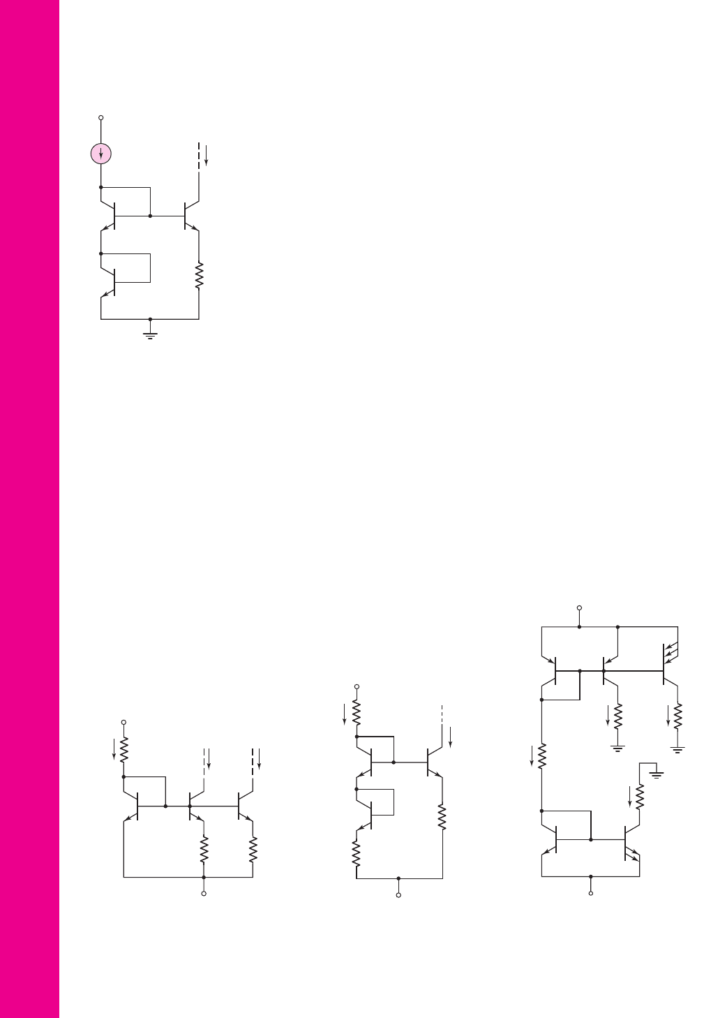
10.34 Consider the circuit in Figure P10.34. The transistors are matched. Assume
that base currents are negligible and that
V
A
=∞
. Using the current–voltage
relationships given by Equations (10.26(a)) and (10.26(b)), show that
I
O
R
E2
− I
REF
R
E1
= V
T
ln
I
REF
I
O
If
R
E1
= R
E2
= 0
and
V
A
=∞
, explain the advantage of this circuit over
the basic two-transistor current source in Figure 10.2(b).
V
+
V
–
R
1
R
E2
R
E1
Q
1
Q
2
I
REF
I
O
V
C2
Figure P10.34
nea80644_ch10_687-752.qxd 6/19/09 4:28 AM Page 741 pmath DATA-DISK:Desktop Folder:18.6.09:MHDQ134-10:
742 Part 2 Analog Electronics
10.35 The modified Widlar current-source circuit shown in Figure P10.34 is
biased at
V
+
= 3
V and
V
−
=−3
V. (a) For
I
S1
= I
S2
= 10
−15
A and
R
E1
= 500
, design the circuit such that
I
REF
= 0.5
mA and
I
O
= 0.2
mA.
Neglect base currents. What are the values of
V
BE1
and
V
BE2
? (b) Repeat
part (a) for
I
S1
= 10
−15
A and
I
S2
= 2 ×10
−15
A.
*10.36 Consider the circuit in Figure P10.36. Neglect base currents and assume
V
A
=∞
. (a) Derive the expression for I
O
in terms of I
REF
and R
E
. (b) De-
termine the value of R
E
such that I
O
=I
REF
=100 μA. Assume
V
BE
= 0.7
V
at a collector current of 1 mA.
10.37 Consider the Widlar current-source circuit with multiple output tran-
sistors shown in Figure P10.37. Assume
V
BE1
= 0.7
V. (a) For circuit
parameters
R
1
= 10
k
,
R
E2
= 1
k
, and
R
E2
= 2
k
, find
I
REF
,
I
O2
, and
I
O3
. (b) Determine new values of
R
E2
and
R
E3
such that
I
O2
= 20 μ
A
and
I
O3
= 80 μ
A.
10.38 Assume that all transistors in the circuit in Figure P10.38 are matched and
that
β =∞
(neglect base currents). (a) Derive an expression for I
O
in terms
of bias voltages and resistor values. (b) Show that if R
1
= R
2
and I
O
= I
REF
,
then
I
O
= (V
+
− V
−
)/2R
E
, which means that the currents are indepen-
dent of V
BE
. (c) For
V
+
=+5
V and
V
−
=−5V
, design the circuit such
that
I
O
= 0.5
mA.
10.39 In the circuit in Figure P10.39, the transistor parameters are:
β =∞
,
V
A
=∞
, and
V
BE
= V
EB
= 0.7
V. Let
R
C1
= 2
k,
R
C2
= 3
k,
R
C3
=
1 k, and R
1
= 12 k. (a) Determine I
O1
, I
O2
, and I
O3
. (b) Calculate
V
CE1
,
V
EC2
, and V
EC3
.
10.40 Consider the circuit in Figure P10.39, with transistor parameters
β =∞
,
V
A
=∞
, and
V
BE
(on) = V
EB
(on)
= 0.7 V. Let
R
1
= 24
k
. (a) Find
I
REF
,
I
O1
,
I
O2
, and
I
O3
. (b) Determine the maximum values of
R
C1
,
R
C2
, and
R
C3
such that
Q
1
,
Q
2
, and
Q
3
remain biased in the forward-active region.
Assume
V
CE
(min) = V
EC
(min) = 0.7
V.
V
+
I
O
Q
1
Q
2
Q
3
R
E
I
REF
Figure P10.36
I
REF
V
+
= 5 V
V
–
= –5 V
R
1
Q
2
I
O2
R
E2
I
O3
R
E3
Q
3
Q
1
Figure P10.37
I
O
R
E
I
REF
Q
1
R
2
R
1
V
+
V
–
Q
2
Q
3
Figure P10.38
R
C2
R
C3
Q
1
I
O1
I
O2
I
REF
I
O3
+10 V
–10 V
R
1
R
C1
Q
R2
Q
2
Q
3
Q
R1
Figure P10.39
nea80644_ch10_687-752.qxd 6/19/09 4:28 AM Page 742 pmath DATA-DISK:Desktop Folder:18.6.09:MHDQ134-10:
10.41 Consider the circuit shown in Figure P10.41. Assume
V
BE
= V
EB
= 0.7
V
for all transistors except Q
5
and let
β =∞
. Determine all collector cur-
rents, and find
V
CE3
,
V
CE5
, and
V
EC7
.
10.42 For the circuit shown in Figure P10.42, assume transistor parameters
V
BE
=
V
EB
= 0.7
V for all transistors except Q
3
and Q
6
, and let
β =∞
. Find the
collector current in each transistor.
Chapter 10 Integrated Circuit Biasing and Active Loads 743
*D10.43 Consider the circuit in Figure P10.43. The transistor parameters are:
β =∞
,
V
A
=∞
, and
V
BE
= 0.7
V. Design the circuit such that the B–E
voltages of Q
1
, Q
2
, and Q
3
are identical to that of Q
R
. What are the values
of I
O1
, I
O2
, and I
O3
?
Section 10.2 FET Current Sources
10.44 Consider the MOSFET current-source circuit in Figure P10.44 with
V
+
=
+2.5 V and R = 15 k. The transistor parameters are
V
TN
= 0.5
V,
k
n
=
80 μA/V
2
,
W/L = 6
, and
λ = 0
. Determine I
REF
, I
O
, and
V
DS2
(sat).
*D10.45 The MOSFET current-source circuit in Figure P10.44 is biased at
V
+
=
2.0 V. The transistor parameters are
V
TN
= 0.5
V,
k
n
= 80
μA/V
2
, and
λ = 0.015
V
−1
. (a) Design the circuit such that I
REF
= 50 μA and the
nominal bias current is I
O
= 100 μA. (b) Find the output resistance R
o
.
(c) Determine the percentage change in I
O
for a change in drain-to-source
voltage of
V
DS2
= 1
V.
I
O1
I
REF
V
+
= 10 V
Q
R
R
1
= 6.3 kΩ
Q
1
Q
2
I
O2
R
ER
= 3 kΩ
R
E1
R
E2
I
O3
R
E3
Q
3
Figure P10.43
R
2
=
1 kΩ
R
3
=
0.8 kΩ
R
E2
=
500 Ω
R
E1
=
300 Ω
Q
5
+10 V
–10 V
+5 V
R
1
=
10 kΩ
Q
2
Q
6
Q
3
Q
4
Q
1
Figure P10.42
Q
2
+5 V
+10 V
–10 V
Q
5
Q
4
Q
3
Q
7
Q
1
Q
6
R
2
=
0.8 kΩ
R
3
=
0.8 kΩ
R
1
=
10 kΩ
R
E
=
500 Ω
Figure P10.41
I
O
R
o
R
V
+
M
1
M
2
I
REF
Figure P10.44
nea80644_ch10_687-752.qxd 6/19/09 4:28 AM Page 743 pmath DATA-DISK:Desktop Folder:18.6.09:MHDQ134-10:
744 Part 2 Analog Electronics
10.46 Consider the basic two-transistor NMOS current source in Figure 10.16.
The circuit parameters are
V
+
=+5
V,
V
−
=−5
V, and
I
REF
= 250
μA.
The transistor parameters are
V
TN
= 1
V,
k
n
= 80
μA/V
2
,and
λ =
0.02
V
−1
. (a) For
(W/L)
1
= (W/L)
2
= 3
, find
I
O
for (i)
V
DS2
= 3
V,
(ii)
V
DS2
= 4.5
V, and (iii)
V
DS2
= 6
V. (b) Repeat part (a) for
(W/L)
1
= 3
and
(W/L)
2
= 4.5
.
10.47 In the two-transistor NMOS current source shown in Figure 10.16, the pa-
rameters are:
V
+
= 3
V,
V
−
=−3
V, and
I
REF
= 0.2
mA. The transistor
parameters are:
V
TN1
= 0.4
V,
K
n1
= 0.2
mA/V
2
, and
λ
1
= λ
2
= 0
. (a) If
V
TN2
= 0.4
V and
K
n2
=
(
0.2 ± 5%
)
mA/V
2
, determine the range in val-
ues of
I
O
. (b) If
K
n2
= 0.2
mA/V
2
and
V
TN2
=
(
0.4 ± 5%
)
V, determine
the range in values of
I
O
.
10.48 Consider the circuit shown in Figure P10.48. Let
I
REF
= 200 μ
A. The tran-
sistor parameters are
K
n1
= K
n2
= 0.2
mA/V
2
,
V
TN1
= V
TN2
= 0.5
V,
and
λ
1
= λ
2
= 0
. (a) If
R
S
= 10
k
, determine
I
O
and
V
GS2
. (b) If
I
O
= 0.5 I
REF
, determine
R
S
and
V
GS2
.
10.49 Consider the two-transistor diode-connected circuit in Figure P10.49. As-
sume that both transistors are biased in the saturation region, and that
g
m1
= g
m2
≡ g
m
and
r
o1
= r
o2
≡ r
o
. Neglect the body effect. Derive the
expression for the output resistance R
o
.
10.50 The circuit parameters for the circuit shown in Figure 10.17 are
V
+
= 1.8
V
and
V
−
=−1.8
V. The transistor parameters are
V
TN
= 0.5
V,
k
n
= 80 μ
A/V
2
, and
λ = 0
. Design the circuit such that
I
O
= 0.15
mA,
I
REF
= 0.5
mA, and
M
2
remains biased in the saturation region for
V
DS2
≥ 1
V.
10.51 The parameters for the circuit in Figure 10.17 are
V
+
=+5
V and
V
−
= 0
. The transistor parameters are
V
TN
= 0.7
V,
k
n
= 60
μA/V
2
, and
λ =
0.015 V
−1
. The transistor width-to-length ratios are
(W/L)
1
= 20
,
(W/L)
2
= 12
, and
(W/L)
3
= 3. Determine (a)
I
REF
, (b) I
O
at
V
DS2
=
1.5 V, and (c) I
O
at
V
DS2
= 3
V.
10.52 Figure P10.52 is a PMOS version of the current-source circuit shown in
Figure 10.17. The transistor M
2
sources a bias current to a load circuit. As-
sume the circuit is biased at
V
+
=+5
V and
V
−
=−5
V, and assume the
transistor parameters are
V
TP
=−0.5
V,
k
p
= 50
μA/V
2
,
(W/L)
1
=
(W/L)
2
= 15
,
(W/L)
3
= 3
, and
λ = 0
. Determine I
REF
, I
O
, and
V
SD2
(sat).
D10.53 The circuit shown in Figure P10.52 is biased at
V
+
=+2
V and
V
−
=
−2
V. Assume the transistor parameters are
V
TP
=−0.35
V,
k
p
=
50 μA/V
2
, and
λ = 0
. Design the circuit such that
I
REF
= 200
μA,
I
O
= 100
μA, and
V
SD2
(sat) = 1.2 V.
10.54 The transistor circuit shown in Figure P10.54 is biased at
V
+
=+5
V
and
V
−
=−5
V. The transistor parameters are
V
TP
=−1.2
V,
k
p
=
80 μ
A/V
2
,
λ = 0
,
(W/L)
1
= (W/L)
2
= 25
, and
(W/L)
3
= (W/L)
4
= 4
.
Determine I
REF
, I
O
, and V
SD2
(sat).
D10.55 Assume the circuit shown in Figure P10.54 is biased at
V
+
= 3
V and
V
−
=−3
V. The transistor parameters are
V
TP
=−0.5
V,
k
p
= 60 μ
A/V
2
,
and
λ = 0
. Design the circuit such that
I
REF
= 250 μ
A,
I
O
= 80 μ
A, and
V
SD2
(
sat
)
= 1.0
V. Assume
M
3
and
M
4
are matched.
10.56 The circuit in Figure P10.56 is a PMOS version of a two-transistor MOS
current mirror. Assume transistor parameters of
V
TP
=−0.4
V,
k
p
= 60 μ
A/V
2
, and
λ = 0
. The transistor width-to-length ratios are
V
+
V
–
M
1
M
3
M
2
I
REF
I
O
Figure P10.52
V
+
= 5 V
I
O
M
1
M
2
R
S
I
REF
Figure P10.48
V
Bias
M
2
M
1
R
o
Figure P10.49
nea80644_ch10_687-752.qxd 6/19/09 4:28 AM Page 744 pmath DATA-DISK:Desktop Folder:18.6.09:MHDQ134-10:
Chapter 10 Integrated Circuit Biasing and Active Loads 745
(
W/L
)
1
= 25
,
(
W/L
)
2
= 15
, and
(
W/L
)
3
= 5
. (a) Determine
I
O
,
I
REF
,
V
SG1
, and
V
SG3
. (b) What is the largest value of
R
such that
M
2
remains
biased in the saturation region?
D10.57 The transistors in Figure P10.56 have the same parameters as in Problem
10.56 except for the
W/L
ratios. Design the circuit such that I
O
= 80 μA,
I
REF
= 220 μ
A, and
V
SD2
(sat) = 0.35
V.
10.58 Consider the NMOS cascode current source in Figure 10.18. The circuit
parameters are
V
+
= 5
V,
V
−
=−5
V, and
I
REF
= 100 μ
A. All transis-
tors are matched with parameters
V
TN
= 0.5
V,
K
n
= 100 μ
A/V
2
, and
λ = 0.02
V
−1
. (a) Determine
I
O
for
V
D4
=−2
V. (b) Determine the per-
cent change in
I
O
as
V
D4
changes from
−2
to
+2
V.
*10.59 Consider the NMOS current source in Figure P10.59. Let
I
REF
= 0.2
mA,
K
n
= 0.2
mA/V
2
,
V
TN
= 1
V, and
λ = 0.02 V
−1
. (All transistors are
matched.) Determine the output resistance looking into the drain of M
6
.
10.60 The transistors in the circuit shown in Figure P10.60 have parameters
V
TN
= 0.4
V,
V
TP
=−0.4
V,
k
n
= 100 μ
A/V
2
,
k
p
= 60 μ
A/V
2
, and
λ
n
= λ
p
= 0
. The transistor width-to-length ratios are
(
W/L
)
1
=
(
W/L
)
2
= 20
,
(
W/L
)
3
= 5
, and
(
W/L
)
4
= 10
. Determine
I
O
,
I
REF
, and
V
DS2
(
sat
)
. What are the values of
V
GS1
, V
GS3
, and
V
SG4
?
D10.61 The transistors in the circuit shown in Figure P10.60 have the same para-
meters as in Problem 10.60 except for the
(
W/L
)
ratios. Design the
circuit such that
I
O
= 50 μ
A,
I
REF
= 500 μ
A,
V
DS2
(sat) = 0.5
V, and
V
GS3
= V
SG4
.
*10.62 A Wilson current mirror is shown in Figure 10.20(a). The parameters are:
V
+
= 5
V,
V
−
=−5
V, and
I
REF
= 80
μA. The transistor parameters
are:
V
TN
= 1
V,
K
n
= 80
μA/V
2
, and
λ = 0.02 V
−1
. Determine I
O
at:
(a)
V
D3
=
−1 V, and (b)
V
D3
=+3
V.
*10.63 Repeat Problem 10.62 for the modified Wilson current mirror in
Figure 10.20(b).
V
+
V
–
M
1
M
3
M
4
M
2
I
REF
I
O
Figure P10.54
V
+
= 3 V
M
1
M
3
M
2
R
I
REF
I
O
Figure P10.56
V
+
M
2
M
1
M
3
M
4
M
5
M
6
I
O
I
REF
Figure P10.59
V
+
= +3 V
V
–
= –3 V
M
4
M
3
M
1
M
2
I
REF
I
O
Figure P10.60
nea80644_ch10_687-752.qxd 6/19/09 4:28 AM Page 745 pmath DATA-DISK:Desktop Folder:18.6.09:MHDQ134-10:
746 Part 2 Analog Electronics
*10.64 Consider the circuit in Figure 10.21 in the text. Assume
I
REF
= 50
μA and
assume transistor parameters of
V
TN
= 0.8
V,
(
1
2
)μ
n
C
ox
= 48 μA/V
2
,
λ = 0
, and
γ = 0
. (a) Find W/L such that
V
DS3
(sat) = 0.2 V. (b) What is
V
GS5
? (c) What is the minimum voltage at the drain of M
1
such that all
transistors remain biased in the saturation region?
10.65 Consider the bias-independent current source in Figure 10.22. Assume
transistor parameters of
V
TN
=+0.5
V,
V
TP
=−0.5
V,
(
1
2
)μ
n
C
ox
=
50 μA/V
2
,
(
1
2
)μ
p
C
ox
= 20 μA/V
2
, and
λ
n
= λ
p
= 0
. The W/L ratios are
given for the
M
1
–M
4
transistors. (a) Determine R such that
I
D1
= I
D2
=
50 μA. (b) What is the minimum bias voltage difference (
V
+
− V
−
) that
must be applied? (c) Determine (W/L)
5
and (W/L)
6
such that
I
O1
=
25
μA and
I
O2
= 75
μA.
D10.66 Consider the multitransistor current source in Figure P10.66. The transis-
tor parameters are
V
TN
= 0.7
V,
k
n
= 80 μ
A/V
2
, and
λ = 0
. Assume
M
3
,
M
4
, and
M
5
are identical. Design the circuit such that
I
REF
= 0.1
mA,
I
O1
= 0.2
mA, and
I
O2
= 0.3
mA.
M
1
I
O1
I
REF
I
O2
M
2
M
3
M
4
M
5
V
+
= 5 V
Figure P10.66
I
O1
=
0.1 mA
I
REF
V
+
= 1.8 V
V
–
= –1.8 V
M
1
M
2
I
O2
=
0.2 mA
M
3
I
O3
=
0.4 mA
M
4
Load
1
Load
2
Load
3
Figure P10.67
D10.67 Consider the circuit shown in Figure P10.67. The transistor parameters are
V
TN
= 0.4
V,
k
n
= 100 μ
A/V
2
, and
λ = 0
. Design the (W/L) ratios of the
transistors such that the total power dissipated in the circuit is 5 mW and
V
DS2
(sat) = 0.4
V.
10.68 The parameters of the transistors in the circuit in Figure P10.68 are
V
TN
= 0.8
V,
V
TP
=−0.8
V,
k
n
= 100 μ
A/V
2
,
k
p
= 60 μ
A/V
2
, and
λ
n
= λ
p
= 0
. The transistor
(
W/L
)
ratios are given in the figure. For
R = 100
k
, determine
I
REF
,
I
1
,
I
2
,
I
3
, and
I
4
.
10.69 Repeat Problem 10.68 if the bias voltages are changed to
V
+
= 5
V and
V
−
=−5
V.
10.70 Consider the circuit shown in Figure P10.70. The NMOS transistor parame-
ters are
V
TN
= 0.4
V,
k
n
= 100
μA/V
2
,
λ
n
= 0
and the PMOS transistor
parameters are
V
TP
=−0.6
V,
k
p
= 40
μA/V
2
,
λ
p
= 0
.Thewidth-to-length
ratios are
(W/L)
1
= 15
,
(W/L)
2
= (W/L)
3
= 9
, and
(W/L)
4
= 20
.
Assume
I
REF
= 200
μA. Determine I
D2
, I
O
, and
V
SD4
(sat).
nea80644_ch10_687-752.qxd 6/19/09 4:28 AM Page 746 pmath DATA-DISK:Desktop Folder:18.6.09:MHDQ134-10:
Chapter 10 Integrated Circuit Biasing and Active Loads 747
10.71 For the circuit shown in Figure P10.70,
I
REF
= 100 μ
A. The transistor
parameters are
V
TN
= 0.4
V,
V
TP
=−0.4
V,
k
n
= 100 μ
A/V
2
,
k
p
=
60 μ
A/V
2
, and
λ
n
= λ
p
= 0
. The transistor width-to-length ratios are
(
W/L
)
1
= 4
,
(
W/L
)
2
= 2.5
,
(
W/L
)
3
= 6
, and
(
W/L
)
4
= 4
. Determine
I
D2
,
I
O
, and all gate-to-source voltages.
D10.72 The parameters of the NMOS transistors in the circuit in Figure P10.72 are
V
TN
= 0.4
V,
k
n
= 100
μA/V
2
,
λ
n
= 0
and the parameters of the PMOS
transistors in the circuit are
V
TP
=−0.6
V,
k
p
= 40
μA/V
2
,
λ
p
= 0
.
Design the circuit such that
I
REF
= 50
μA,
I
O1
= 120
μA,
I
D3
= 25
μA,
I
O2
=
150 μA,
V
SD2
(sat) = 0.35
V, and
V
DS5
(sat) = 0.35
V.
10.73 For the JFET in Figure P10.73, the parameters are:
I
DSS
= 2
mA,
V
P
=
−2 V, and
λ = 0.05 V
−1
. Determine I
O
for: (a)
V
D
=−5
V, (b)
V
D
= 0
V,
and (c)
V
D
=+5
V.
D10.74 A JFET circuit is biased with the current source in Figure P10.74. The
transistor parameters are:
I
DSS
= 4
mA,
V
P
=−4
V, and
λ = 0
. Design
the circuit such that
I
O
= 2
mA. What is the minimum value of V
D
such
that the transistor is biased in the saturation region?
I
1
I
2
I
3
I
4
I
REF
R
V
+
= +12 V
V
–
= –12 V
4
0.8
1
0.2
1.25
1
1
1
1
1
1
1
Figure P10.68
I
O
M
1
M
2
M
3
M
4
I
REF
V
+
Figure P10.70
I
REF
M
1
M
3
M
4
M
5
I
O2
I
O1
M
2
R
+1.75 V
–1.75 V
Figure P10.72
I
O
V
D
–10 V
Figure P10.73
I
O
V
D
R
Figure P10.74
nea80644_ch10_687-752.qxd 6/19/09 4:28 AM Page 747 pmath DATA-DISK:Desktop Folder:18.6.09:MHDQ134-10: