Neamen D. Microelectronics: Circuit Analysis and Design
Подождите немного. Документ загружается.

788 Part 2 Analog Electronics
The common-mode rejection ratio is then
CMRR =
A
d
A
cm
=
g
m
R
D
(R
D
/R
o
)
(11.86)
This result is essentially the same as the BJT diff-amp.
Effect of g
m
Mismatch—Two-Sided Output
We can consider the effect of transistor mismatch by considering the effect of a
mismatch in the transconductance g
m
. We assume g
m1
and g
m2
are the transconduc-
tance parameters of the two transistors in the diff-amp. We will assume that we can
write
g
m1
= g
m
+g
m
and
g
m2
= g
m
−g
m
.
Again, using the small-signal equiva-
lent circuit shown in Figure 11.23, we find the differential-mode voltage gain is
A
d
= g
m
R
D
(11.87(a))
and the common-mode gain is
A
cm
=
R
D
(2g
m
)
1 + 2R
o
g
m
(11.87(b))
The common-mode rejection ratio now becomes
CMRR =
A
d
A
cm
=
1 + 2R
o
g
m
2(g
m
/g
m
)
(11.88)
The CMRR of mismatched elements in the MOSFET diff-amp is identical with the
results of mismatched elements in the BJT diff-amp.
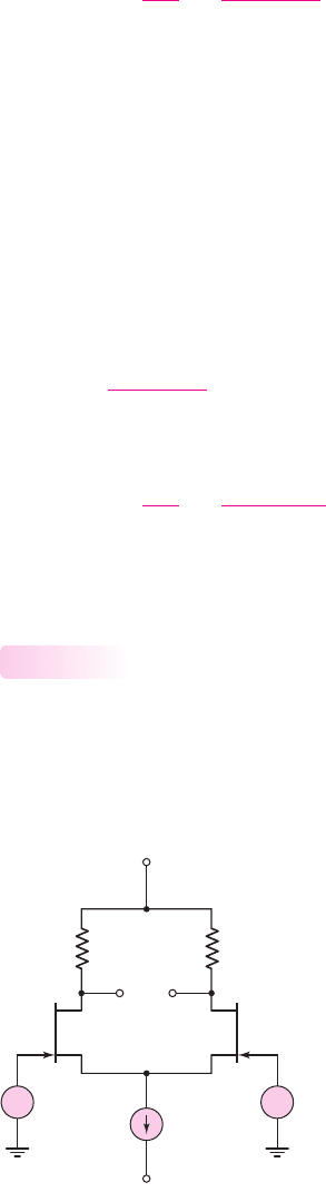
JFET Differential Amplifier
Figure 11.25 shows a basic JFET differential pair biased with a constant-current
source. If a pure differential-mode input signal is applied such that
v
G1
=+v
d
/2
and
v
G2
=−v
d
/2
, then drain currents I
D1
and I
D2
increase and decrease, respectively, in
exactly the same way as in the MOSFET diff-amp.
11.3.5
V
+
V
–
R
D
R
D
I
Q
v
O1
v
O2
Q
1
Q
2
v
G1
v
G2
+
–
+
–
Figure 11.25 Basic JFET
differential pair configuration
nea80644_ch11_753-850.qxd 6/19/09 4:37 AM Page 788 pmath DATA-DISK:Desktop Folder:18.6.09:MHDQ134-11:
Chapter 11 Differential and Multistage Amplifiers 789
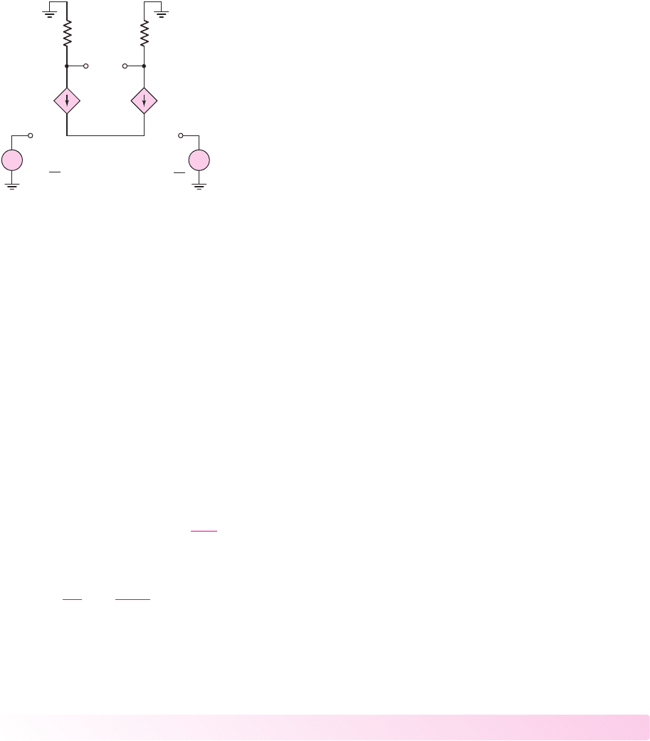
We can determine the differential-mode voltage gain by analyzing the small-signal
equivalent circuit. Figure 11.26 shows the equivalent circuit, with the output resistance
of the constant-current source and the small-signal resistances of Q
1
and Q
2
assumed to
be infinite. The small-signal equivalent circuit of the JFET diff-amp is identical to that
of the MOSFET diff-amp in Figure 11.23 for the case when the current-source output
resistance is infinite. A KCL equation at the common-source node, in phasor notation, is
g
m
V
gs1
+ g
m
V
gs2
= 0
(11.89(a))
or
V
gs1
=−V
gs2
(11.89(b))
The differential-mode input voltage is
V
d
≡ V
1
− V
2
= V
gs1
− V
gs2
=−2V
gs2
(11.90)
A one-sided output at V
o2
is given by
V
o2
=−g
m
V
gs2
R
D
=−g
m
−V
d
2
R
D
(11.91)
and the differential-mode voltage gain is
A
d
=
V
o2
V
d
=+
g
m
R
D
2
(11.92)
The expression for the differential-mode voltage gain for the JFET diff-amp
(Equation (11.92)) is exactly the same as that of the MOSFET diff-amp (Equa-
tion 11.82(a)). If the constant-current source output resistance is finite, then the JFET
diff-amp will also have a nonzero common-mode voltage gain.
Test Your Understanding
TYU 11.7 The circuit parameters of the diff-amp shown in Figure 11.19 are
V
+
= 3
V,
V
−
=−3
V,
I
Q
= 0.40
mA, and
R
D
= 7.5
k
. The transistor parameters
are
V
TN
= 0.5
V,
k
n
= 100 μ
A/V
2
, and
λ = 0
. (a) Design the transistor
W/L
ratio
such that the differential voltage gain is
A
d
= 12
. (b) What is the maximum positive
common-mode voltage that can be applied such that the transistors remain biased in
the saturation region. (Ans. (a)
W/L = 256
, (b)
v
cm
= 2
V)
R
D
R
D
V
o1
V
o2
g
m
V
gs1
g
m
V
gs2
V
gs1
+–
V
gs2
+–
V
d
2
V
1
=
V
d
2
V
2
= –
+
–
+
–
Figure 11.26 Small-signal equivalent
circuit, JFET differential amplifier
nea80644_ch11_753-850.qxd 6/19/09 4:37 AM Page 789 pmath DATA-DISK:Desktop Folder:18.6.09:MHDQ134-11:
790 Part 2 Analog Electronics
TYU 11.8 Consider the differential amplifier in Figure 11.20. The transistor parame-
ters are given in Example 11.8, except that
λ = 0.02 V
−1
for M
3
and M
4
. Determine
the differential voltage gain
A
d
= v
o2
/v
d
, the common-mode gain
A
cm
= v
o2
/v
cm
,
and the CMRR
dB
. (Ans.
A
d
= 2.74
,
A
cm
=−0.0925
, CMRR
dB
= 29.4
dB)
TYU 11.9 The diff-amp in Figure 11.19 is biased at
I
Q
= 100 μ
A. The transistor
parameters are
k
n
= 100 μ
A/V
2
and
W/L = 10
. (a) If the output resistance of the
current source is
R
o
= 1
M
, determine the common-mode rejection ratio
CMRR
dB
. (b) Determine the required value of
R
o
such that
CMRR
dB
= 80
dB.
(Ans. (a)
CMRR
dB
= 50
dB, (b)
R
o
= 31.6
M
)
*TYU 11.10 The differential amplifier in Figure 11.20 is to be redesigned.The current-
source biasing is to be replaced with the cascode current source in Figure 11.24. The
reference current is
I
REF
= 100 μA
and
λ
for transistors in the current source circuit
is 0.01 V
−1
. The parameters of the differential pair M
1
and M
2
are the same as
described in Example 11.8. The range of the common-mode input voltage is to
be
−4 ≤ v
cm
≤+4V
. Redesign the diff-amp to achieve the highest possible
differential-mode voltage gain. Determine the values of A
d
, A
cm
, and CMRR
dB
. (Ans.
A
d
= 9.90
,
A
cm
= 0.0003465
, CMRR
dB
= 89.1
dB)
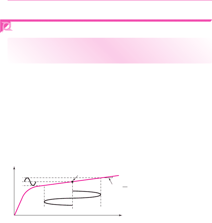
11.4 DIFFERENTIAL AMPLIFIER WITH ACTIVE LOAD
Objective: • Analyze the characteristics of BJT and FET differential
amplifiers with active loads.
In Chapter 10, we considered an active load in conjunction with a simple transis-
tor amplifier. Active loads can also be used in diff-amp circuits to increase the
differential-mode gain.
Active loads are essentially transistor current sources used in place of resistive
loads. The transistors in the active load circuit are biased at a Q-point in the forward-
active mode as shown in Figure 11.27. A change in collector current is induced by the
differential-pair, which, in turn, produces a change in the emitter–collector voltage as
shown in the figure. The relation between the change in current and change in volt-
age is proportional to the small-signal output resistance r
o
of the transistor. The value
of r
o
is, in general, much larger than that of a discrete resistive load, so the small-
signal voltage gain will be larger with the active load.
V
EC
Q-point
I
C
1
r
o
slope =
I
B
= constan
t
Figure 11.27 Current–voltage characteristic of active load device
nea80644_ch11_753-850.qxd 6/19/09 4:37 AM Page 790 pmath DATA-DISK:Desktop Folder:18.6.09:MHDQ134-11:
Chapter 11 Differential and Multistage Amplifiers 791
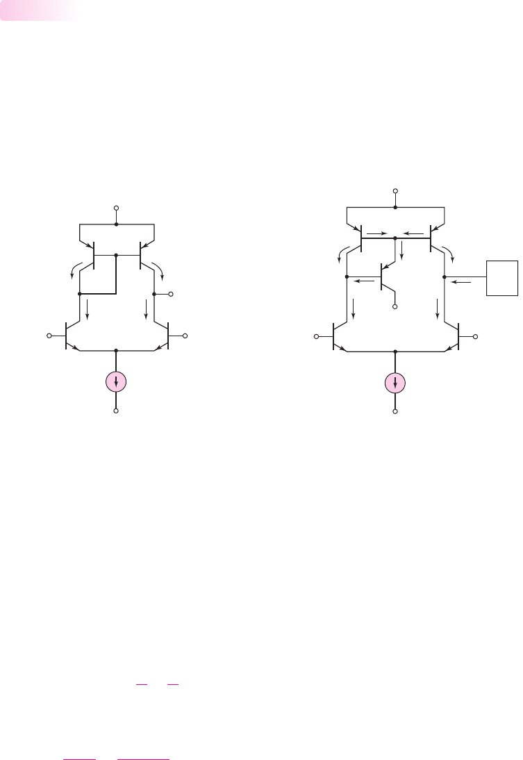
BJT Diff-Amp with Active Load
Figure 11.28 shows a differential amplifier with an active load. Transistors Q
1
and Q
2
are the differential pair biased with a constant current I
Q
, and transistors Q
3
and Q
4
form the load circuit. From the collectors of Q
2
and Q
4
, we obtain a one-sided output.
If we assume all transistors are matched, then a pure applied common-mode
voltage means that
v
B1
= v
B2
= v
CM
, and current I
Q
splits evenly between Q
1
and
Q
2
. Neglecting base currents,
I
4
= I
3
through the current-source circuit and
I
1
=
I
2
= I
3
= I
4
= I
Q
/2
with no load connected at the output.
11.4.1
V
+
V
–
Q
3
Q
4
I
3
I
4
I
1
I
2
v
B1
= v
CM
v
B2
= v
C
M
v
O
Q
1
Q
2
I
Q
Figure 11.28 BJT differential amplifier with
active load
I
2
I
1
V
+
V
–
V
–
I
B3
I
B4
Q
3
Q
4
I
3
I
4
I
E5
I
B5
Q
5
I
O
Gain
stage
v
B1
= v
CM
v
B2
= v
CM
Q
1
Q
2
I
Q
Figure 11.29 BJT differential amplifier with three-
transistor active load and second gain stage
In actual diff-amp circuits, base currents are not zero. In addition, a second
amplifier stage is connected at the diff-amp output. Figure 11.29 shows a diff-amp
with an active load circuit, corresponding to a three-transistor current source, as well
as a second amplifying stage. In general, the common–emitter current gain
β
is a
function of collector current, as was shown in Figure 6.21(c). However, for simplic-
ity, we assume all transistor current gains are equal, even though the current level in
Q
5
is much smaller than in the other transistors. Current I
O
is the dc bias current from
the gain stage. Assuming all transistors are matched and
v
B1
= v
B2
= v
CM
, current
I
Q
splits evenly and
I
1
= I
2
. To ensure that Q
2
and Q
4
are biased in the forward-
active mode, the dc currents must be balanced, or
I
3
= I
4
. We see that
I
E5
= I
B3
+ I
B4
=
I
3
β
+
I
4
β
(11.93)
Then
I
B5
=
I
E5
1 + β
=
I
3
+ I
4
β(1 +β)
(11.94)
If the base currents and I
O
are small, then
I
3
+ I
4
∼
=
I
Q
(11.95)
nea80644_ch11_753-850.qxd 6/19/09 4:37 AM Page 791 pmath DATA-DISK:Desktop Folder:18.6.09:MHDQ134-11:
792 Part 2 Analog Electronics
Therefore,
I
B5
∼
=
I
Q
β(1 +β)
(11.96)
For the circuit to be balanced, that is, for
I
1
= I
2
and
I
3
= I
4
, we must have
I
O
= I
B5
=
I
Q
β(1 +β)
(11.97)
Equation (11.97) implies that the second amplifying stage must be designed and
biased such that the direction of the dc bias current is as shown and is equal to the
result of Equation (11.97). To illustrate this condition, we will analyze a second
amplifying stage using a Darlington pair, later in this chapter.
Small-Signal Analysis of BJT Active Load
Figure 11.30 shows a diff-amp with a three-transistor active load circuit. The resis-
tance R
L
represents the small-signal input resistance of the gain stage. We will assume
that a pure differential-mode input voltage is applied as shown in the figure. From
previous results, we know that the common-emitter terminals of Q
1
and Q
2
are at sig-
nal ground. The signal voltage at the base of Q
1
produces a signal collector current
i
1
= (g
m
v
d
)/2
, where g
m
is the transistor transconductance for both Q
1
and Q
2
.
Assuming the base currents are negligible, a signal current
i
3
= i
1
is induced in Q
3
,
and the current mirror produces a signal current i
4
equal to i
3
. The signal voltage at the
base of Q
2
produces a signal collector current
i
2
= (g
m
v
d
)/2
, with the direction
shown. The two signal currents, i
2
and i
4
, add to produce a signal current in the load
resistance R
L
. The discussion is a first-order evaluation of the circuit operation.
11.4.2
+
–
V
+
V
–
V
–
Q
3
Q
5
Q
4
Q
1
Q
2
i
3
i
4
=
i
2
=i
1
=
g
m
v
d
2
g
m
v
d
2
g
m
v
d
2
v
o
i
o
R
L
i
b1
i
b2
v
d
2
v
d
2
I
Q
C
C
+
–
–
+
Signal
ground
Figure 11.30 BJT differential amplifier with three-transistor active load, showing
the signal currents
From the above discussion, we know the induced currents in Q
2
and Q
4
. To
more accurately determine the output voltage, we need to consider the equivalent
small-signal collector–emitter output circuit of the two transistors. Figure 11.31(a)
nea80644_ch11_753-850.qxd 6/19/09 4:37 AM Page 792 pmath DATA-DISK:Desktop Folder:18.6.09:MHDQ134-11:
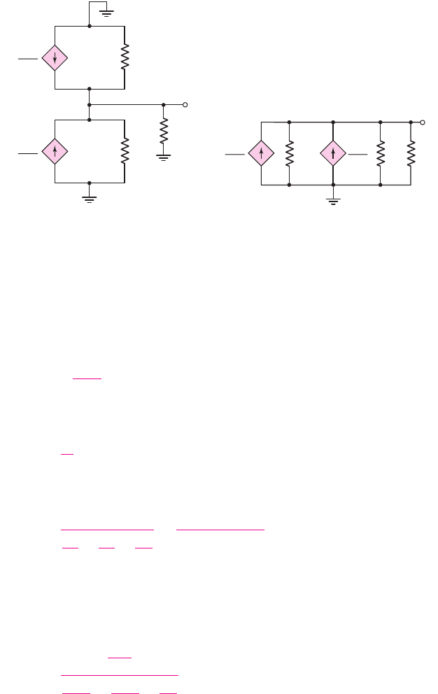
Chapter 11 Differential and Multistage Amplifiers 793
shows the small-signal equivalent circuit at the collector nodes of Q
2
and Q
4
. The
circuit can be rearranged to combine the signal grounds at a common point, as in
Figure 11.31(b). From this figure, we determine that
v
o
= 2
g
m
v
d
2
(r
o2
r
o4
R
L
)
(11.98)
and the small-signal differential-mode voltage gain is
A
d
=
v
o
v
d
= g
m
(r
o2
r
o4
R
L
)
(11.99)
Equation (11.99) can be rewritten in the form
A
d
=
g
m
1
r
o2
+
1
r
o4
+
1
R
L
=
g
m
g
o2
+ g
o4
+ G
L
(11.100)
We recall that
g
m
= I
Q
/2V
T
, r
o2
= V
A2
/I
2
, and
r
o4
= V
A4
/I
4
. The parameters g
o2
,
g
o4
, and G
L
are the corresponding conductances. Assuming
I
2
= I
4
= I
Q
/2
, we can
write Equation (11.100) in the form
A
d
=
I
Q
2V
T
I
Q
2V
A2
+
I
Q
2V
A4
+
1
R
L
(11.101)
This expression of the differential-mode voltage gain of the diff-amp with an active
load is very similar to that obtained in the last chapter for a simple amplifier with an
active load.
The output resistance looking back into the common collector node is
R
o
=
r
o2
r
o4
. To minimize loading effects, we need
R
L
> R
o
. However, since R
o
is gener-
ally large for active loads, we may not be able to satisfy this condition. We can de-
termine the severity of the loading effect by comparing R
L
and R
o
.
g
m
v
d
2
g
m
v
d
2
i
4
=
g
m
v
d
2
g
m
v
d
2
i
2
=
r
o4
v
o
R
L
r
o2
v
o
r
o4
r
o2
R
L
(a) (b)
Figure 11.31 (a) Small-signal equivalent circuit BJT differential amplifier with active load
and (b) rearrangement of small-signal equivalent circuit
nea80644_ch11_753-850.qxd 6/19/09 4:37 AM Page 793 pmath DATA-DISK:Desktop Folder:18.6.09:MHDQ134-11:

794 Part 2 Analog Electronics
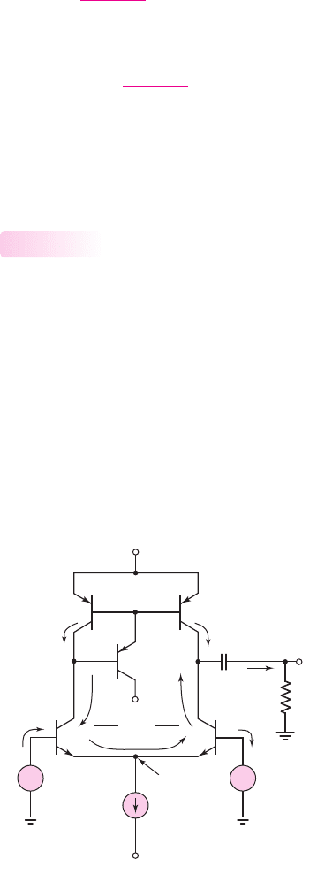
EXAMPLE 11.10
Objective: Determine the differential-mode gain of a diff-amp with an active load,
taking loading effects into account.
Consider the diff-amp in Figure 11.30, biased with
I
Q
= 0.20
mA. Assume an
Early voltage of
V
A
= 100
V for all transistors. Determine the open-circuit (
R
L
=∞
)
differential-mode voltage gain, as well as the differential-mode voltage gain when
R
L
= 100 k
.
Solution: From Equation (11.101), the open-circuit voltage gain becomes
A
d
=
1
V
T
1
V
A2
+
1
V
A4
=
1
0.026
1
100
+
1
100
= 1923
When
R
L
= 100 k
, the voltage gain is
A
d
=
0.20 × 10
−3
2(0.026)
0.20 × 10
−3
2(100)
+
0.20 × 10
−3
2(100)
+
1
100 × 10
3
which can be written
A
d
=
0.20
2(0.026)
0.20
2(100)
+
0.20
2(100)
+
1
100
=
3.85
0.001 + 0.001 +0.01
= 321
An inspection of this last equation shows that the external load factor, 1/R
L
, domi-
nates the denominator term and thus has a tremendous influence on the gain.
Comment: The open-circuit differential-mode voltage gain, for a diff-amp with an
active load, is large. However, a finite load resistance R
L
causes severe loading
effects, as shown in this example. A
100 k
load caused almost an order of magni-
tude decrease in the gain.
EXERCISE PROBLEM
Ex 11.10: The diff-amp circuit in Figure 11.30 is biased at
I
Q
= 0.4
mA. The
transistor parameters are
β = 120
,
V
A1
= V
A2
= 150
V, and
V
A3
= V
A4
= 90
V.
(a) Determine the open-circuit (
R
L
=∞)
differential-mode voltage gain. (b) Find
the differential-mode voltage gain when
R
L
= 250
k
. (c) Determine the
differential-mode input resistance. (d) Find the output resistance looking back
from the load
R
L
. (Ans. (a) 2163, (b) 1018, (c) 31.2 k
, (d) 281 k
)
MOSFET Differential Amplifier with Active Load
We can use an active load in conjunction with a MOSFET differential pair, as we did
for the bipolar differential amplifier. Figure 11.32 shows a MOSFET diff-amp with
an active load. Transistors M
1
and M
2
are n-channel devices and form the differential
11.4.3
nea80644_ch11_753-850.qxd 6/19/09 4:37 AM Page 794 pmath DATA-DISK:Desktop Folder:18.6.09:MHDQ134-11:
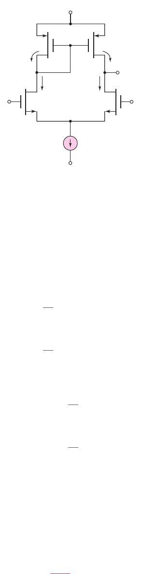
Chapter 11 Differential and Multistage Amplifiers 795
pair biased with I
Q
. The load circuit consists of transistors M
3
and M
4
, both p-channel
devices, connected in a current mirror configuration. A one-sided output is taken
from the common drains of M
2
and M
4
. When a common-mode voltage of
v
1
= v
2
= v
cm
is applied, the current I
Q
splits evenly between M
1
and M
2
, and
i
D1
= i
D2
= I
Q
/2
. There are no gate currents; therefore,
i
D3
= i
D1
and
i
D4
= i
D2
.
If a small differential-mode input voltage
v
d
= v
1
−v
2
is applied, then from
Equation (11.66) and (11.67), we can write
i
D1
=
I
Q
2
+i
d
(11.102(a))
and
i
D2
=
I
Q
2
−i
d
(11.102(b))
where i
d
is the signal current. For small values of v
d
, we have
i
d
= (g
m
v
d
)/2
. Since
M
1
and M
3
are in series, we see that
i
D3
= i
D1
=
I
Q
2
+i
d
(11.103)
Finally, the current mirror consisting of M
3
and M
4
produces
i
D4
= i
D3
=
I
Q
2
+i
d
(11.104)
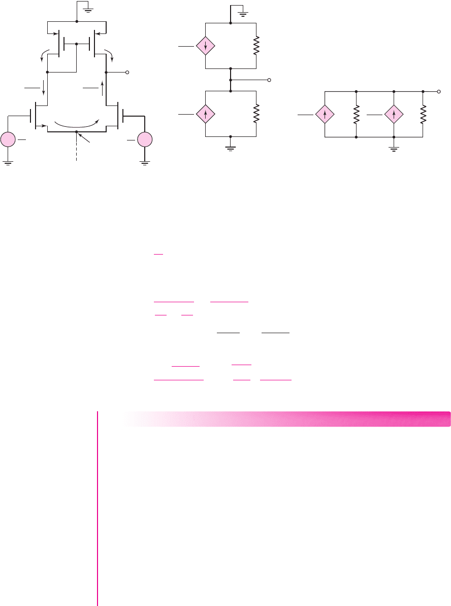
Figure 11.33 is the ac equivalent circuit of the diff-amp with active load, showing the
signal currents. The negative sign for i
D2
in Equation (11.102(b)) shows up as a
change in current direction in M
2
, as indicated in the figure.
Figure 11.34(a) shows the small-signal equivalent circuit at the drain node of M
2
and M
4
. If the output is connected to the gate of another MOSFET, which is equiva-
lent to an infinite impedance at low frequency, the output terminal is effectively an
open circuit. The circuit can be rearranged by combining the signal grounds at a
common point, as shown in Figure 11.34(b). Then,
v
o
= 2
g
m
v
d
2
(r
o2
r
o4
)
(11.105)
V
+
V
–
M
3
M
1
M
2
M
4
i
D3
i
D4
i
D1
i
D2
v
O
v
1
v
2
I
Q
Figure 11.32 MOSFET differential amplifier with active load
nea80644_ch11_753-850.qxd 6/19/09 4:37 AM Page 795 pmath DATA-DISK:Desktop Folder:18.6.09:MHDQ134-11:
796 Part 2 Analog Electronics
and the small-signal differential-mode voltage gain is
A
d
=
v
o
v
d
= g
m
(r
o2
r
o4
)
(11.106)
Equation (11.106) can be rewritten in the form
A
d
=
g
m
1
r
o2
+
1
r
o4
=
g
m
g
o2
+ g
o4
(11.107)
If we recall that
g
m
= 2
√
K
n
I
D
=
2K
n
I
Q
,
g
o2
= λ
2
I
DQ2
= (λ
2
I
Q
)/2
, and
g
o4
=
λ
4
I
DQ4
= (λ
4
I
Q
)/2
, then Equation (11.107) becomes
A
d
=
2
2K
n
I
Q
I
Q
(λ
2
+λ
4
)
= 2
2K
n
I
Q
·
1
λ
2
+λ
4
(11.108)
DESIGN EXAMPLE 11.11
Objective: Design a MOSFET diff-amp with the configuration in Figure 11.32 to
meet the specifications of the experimental system in Example 11.4.
Design Approach: We need not only to try to obtain the necessary differential-mode
gain and minimize the common-mode gain in our design, but we must also be
cognizant of the swing in the output voltage. In the circuit in Figure 11.32, if the cor-
responding PMOS and NMOS transistors are matched, then the quiescent value of
V
SD4
is equal to
V
SG4
= V
SG3
. As the signal output voltage increases, the source-to-
drain voltage of M
4
decreases. The minimum value of this voltage such that M
4
remains biased in the saturation region is
V
SD4
(min) = V
SD4
(sat) = V
SG
+ V
TP
.
This means that the maximum swing in the output voltage is equal to the magnitude
of the threshold voltage of M
4
. In this example, the maximum swing in the output
voltage is 0.8 V, so that the magnitude of the threshold voltages of the PMOS devices
must be greater than 0.8 V. Assume that NMOS devices are available with the fol-
lowing parameters:
V
TN
= 0.5
V,
k
n
= 80 μA/V
2
, and
λ
n
= 0.02 V
−1
. Assume that
(a)
(b)
r
o4
r
o2
v
o
g
m
v
d
2
g
m
v
d
2
v
o
g
m
v
d
2
g
m
v
d
2
r
o4
r
o2
Figure 11.34 (a) Small-signal equivalent circuit, MOSFET differential
amplifier with active load and (b) rearranged small-signal equivalent
circuit
v
d
2
M
1
M
2
M
3
M
4
i
d
i
d
v
o
i
d
=
g
m
v
d
2
i
d
=
g
m
v
d
2
+
–
v
d
2
+
–
Signal
ground
Figure 11.33 The ac equivalent circuit,
MOSFET differential amplifier with
active load
nea80644_ch11_753-850.qxd 6/19/09 4:37 AM Page 796 pmath DATA-DISK:Desktop Folder:18.6.09:MHDQ134-11:
Chapter 11 Differential and Multistage Amplifiers 797
PMOS devices are available with the following parameters:
V
TP
=−1.0
V,
k
p
=
40 μA/V
2
, and
λ
p
= 0.02 V
−1
. Choose supply voltages of
±5
V and choose a bias
current of approximately
I
Q
= 200 μA
.
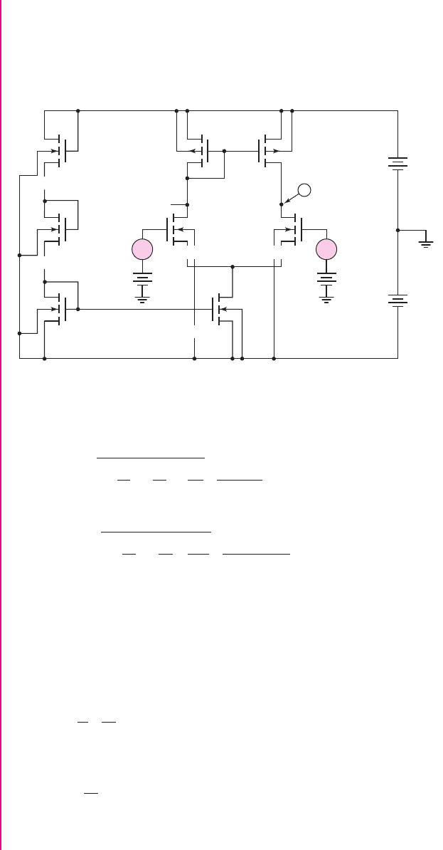
Figure 11.35 is the diff-amp and current-source network used for the design in
this example.
M
6
M
7
M
8
MbreakN-X5
MbreakP
Mbreakp
MbreakN-X4
MbreakN-X3
MbreakN-X2
MbreakN-X1 MbreakN-X
M
5
M
4
+
~
–
+
~
–
M
2
M
3
M
1
V
V
3
4 mV
2.5 V
0
V
6
0
0
V
5
V
1
V
2
V
4
+
–
2.5 V
–4 mV
+
–
5 V
+
–
5 V
+
–
Figure 11.35 CMOS differential amplifier and current source network for Example 11.11
Design, Differential Amplifier: Differential-Mode Gain:
From Equation (11.108),
the differential-mode gain is
A
d
= 2
2
k
n
2
W
L
n
1
I
Q
·
1
λ
n
+λ
p
or
100 = 2
2
80
2
W
L
1
200
·
1
0.02 + 0.02
which yields a width-to-length ratio of
(W/L)
n
= 10
for the NMOS differential pair.
Since the width-to-length ratios of the other transistors do not directly affect the gain
of the diff-amp, we may arbitrarily choose width-to-length ratios of 10 for all other
transistors except M
5
and M
6
. The W/L ratio of 10 means that the other devices are
reasonably small and do not lead to a large circuit area.
Design, Current-Source Network: For the transistor M
3
in the current source, we have
I
Q
=
k
2
·
W
L
· (V
GS3
− V
TN
)
2
or
200 =
80
2
(10)(V
GS3
−0.5)
2
which means that the required gate-to-source voltage of M
3
is
V
GS3
= 1.21
V. We
may choose M
4
and M
3
to be identical so that the current in the reference portion of
nea80644_ch11_753-850.qxd 6/19/09 5:35 AM Page 797 pmath DATA-DISK:Desktop Folder:18.6.09:MHDQ134-11: