Neamen D. Microelectronics: Circuit Analysis and Design
Подождите немного. Документ загружается.


798 Part 2 Analog Electronics
the circuit is also
200 μA
. Assuming that M
5
and M
6
are identical, then each transis-
tor must have a gate-to-source voltage of
V
GS5
= V
GS6
= (10 −1.21)/2
∼
=
4.4V
The width-to-length of these transistors is now found from
I
REF
= I
Q
=
k
n
2
·
W
L
5
(V
GS5
− V
TN
)
2
or
200 =
80
2
·
W
L
5
(4.4 − 0.5)
2
which yields
(W/L)
5
= (W/L)
6
= 0.33
Computer Simulation Verification: The circuit in Figure 11.35 was used in the com-
puter simulation verification. In the hand design, the finite output resistance (lambda
parameter) was neglected in the dc calculations. These parameters became important
in the actual design and in the actual currents developed in the circuit. For
(W/L)
5
= (W/L)
6
= 0.75
, the reference current is
I
REF
= 231 μA
and the bias
current is
I
Q
= 208 μA
.
The differential-mode voltage gain is approximately 102 so that the signal out-
put voltage is 0.82 V for a differential-mode input signal voltage of 8 mV. The
common-mode output signal is approximately 0.86 mV, which is well within the
specified 10 mV maximum value.
Design Pointer: The body effect has been neglected in this design. In actual inte-
grated circuits, the differential pair transistors may actually be fabricated within their
own p-type substrate region (for NMOS devices). This p-type substrate region is then
directly connected to the source terminals so that the body effect in the NMOS
differential pair devices can be neglected.
EXERCISE PROBLEM
Ex 11.11: Determine I
REF
, I
Q
, and A
d
of the diff-amp designed in Example 11.11
for the case when the bias voltages are changed to
V
+
=+3
Vand
V
−
=−3
V.
(Ans.
I
REF
= I
Q
= 56.37 μA
,
A
d
= 188
)
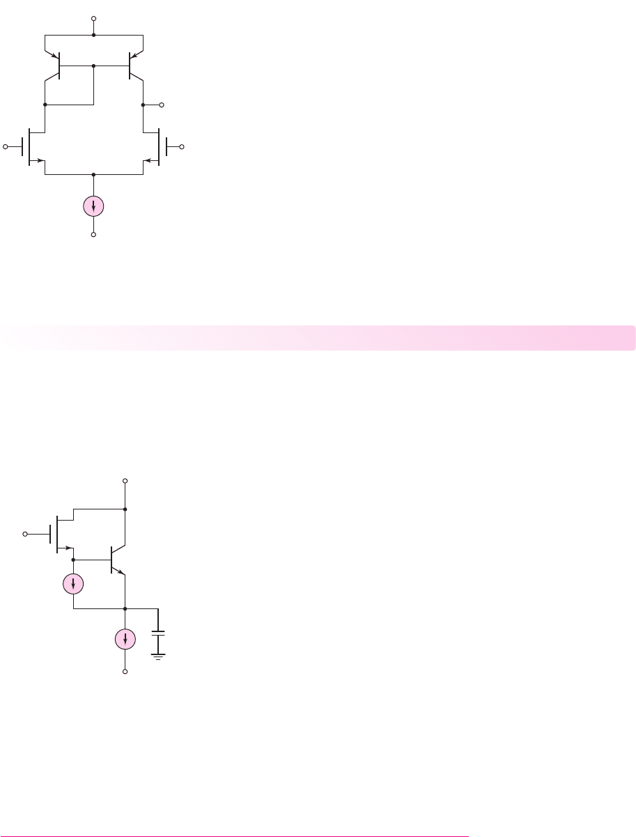
MOSFET Diff-Amp with Cascode Active Load
The differential-mode voltage gain is proportional to the output resistance looking into
the active load transistor. The voltage gain can be increased, therefore, if the output
resistance can be increased. An increase in output resistance can be achieved by using,
for example, a cascode active load. This configuration is shown in Figure 11.36.
The output resistance R
o
was considered in the last section in the discussion
of the cascode current source. As applied to Figure 11.36, the output resistance is
given by
R
o
= r
o4
+r
o6
(1 + g
m
r
o4
)
∼
=
g
m
r
o4
r
o6
(11.109)
11.4.4
nea80644_ch11_753-850.qxd 6/19/09 4:37 AM Page 798 pmath DATA-DISK:Desktop Folder:18.6.09:MHDQ134-11:

Chapter 11 Differential and Multistage Amplifiers 799
The small-signal differential-mode voltage gain is then
A
d
=
v
o
v
d
= g
m
(r
o2
R
o
)
(11.110)
EXAMPLE 11.12
Objective: Calculate the differential-mode voltage gain of a MOSFET diff-amp
with a cascode active load.
Consider the diff-amp shown in Figure 11.36. Assume the circuit and transistor
parameters are the same as in Example 11.11.
Solution: The transistor transconductance is
g
m
= 2
K
n
I
DQ
= 2
0.08
2
(10)(0.1) = 0.40 mA/V
The output resistance of the individual transistors is
r
o
=
1
λI
DQ
=
1
(0.02)(0.1)
= 500 k
The output resistance of the cascode active load is then
R
o
= r
o4
+r
o6
(1 + g
m
r
o4
) = 0.5 +0.5[1 +(0.40)(500)] = 101 M
The differential-mode voltage gain is then found to be
A
d
= g
m
(r
o2
R
o
) = (0.40)(500101000) = 200
Comment: Since
R
o
r
o2
, the voltage gain is now essentially equal to
A
d
= g
m
r
o2
which is twice as large as the gain calculated in Example 11.11.
V
+
V
–
M
5
M
3
M
4
M
2
r
o2
R
o
M
1
I
Q
v
1
v
2
v
o
M
6
Figure 11.36 MOSFET diff-amp with cascode active load
nea80644_ch11_753-850.qxd 6/19/09 4:37 AM Page 799 pmath DATA-DISK:Desktop Folder:18.6.09:MHDQ134-11:
800 Part 2 Analog Electronics
EXERCISE PROBLEM
Ex 11.12: The parameters of the circuit and transistors in Figure 11.36 are the
same as described in Example 11.12 except for M
1
and M
2
. Assume
k
n1
= k
n2
=
80 μA/V
2
. Determine
(W/L)
1
= (W/L)
2
such that
A
d
= 400
. (Ans.
(W/L)
1
=
(W/L)
2
= 40
)
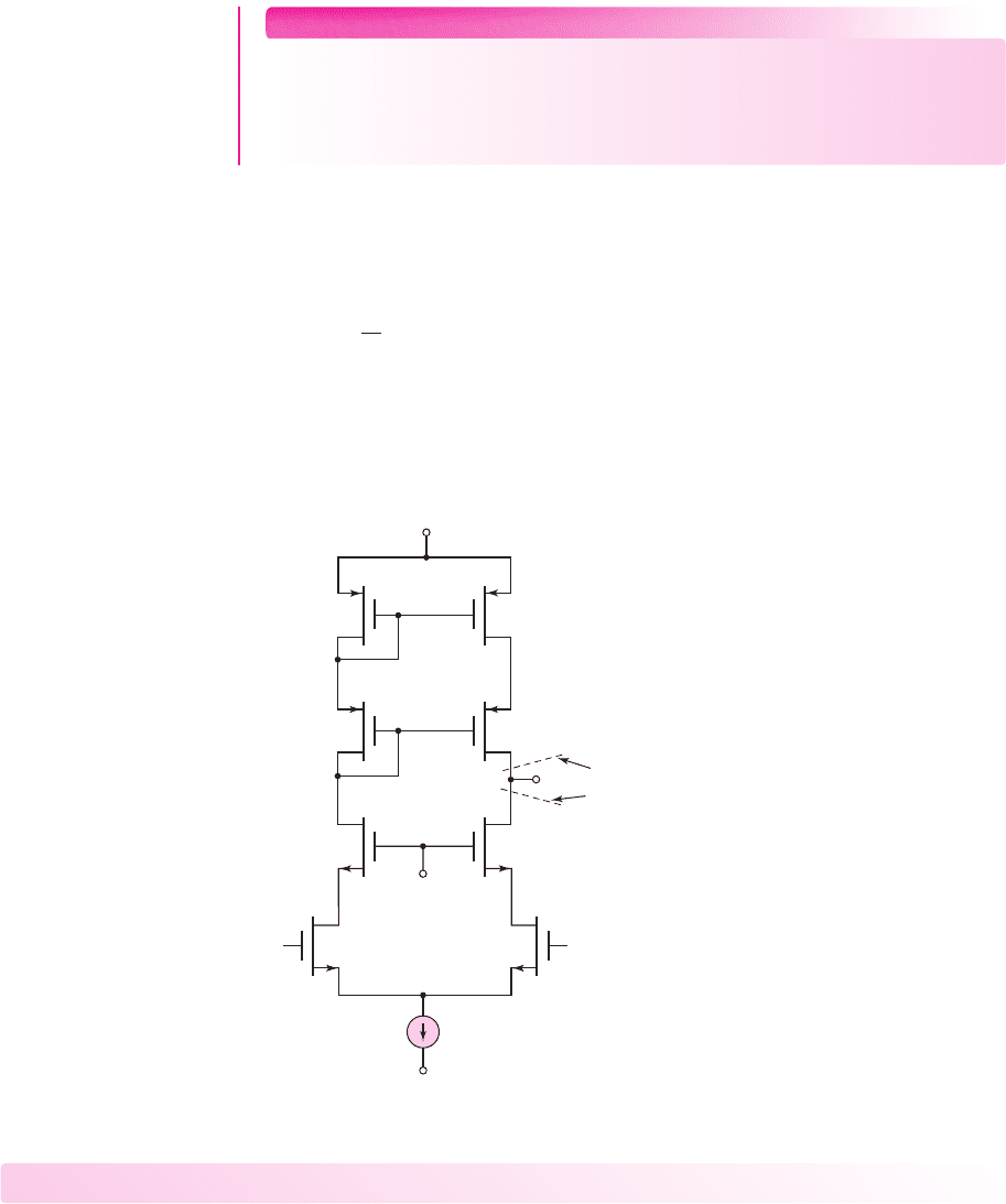
The differential-mode voltage gain can be further increased by incorporating a
cascode configuration in the differential pair as well as in the active load. One such
example is shown in Figure 11.37. Transistors M
3
and M
4
are the cascode transistors
for the differential pair M
1
and M
2
. The differential-mode voltage gain is now
A
d
=
v
o
v
d
= g
m
(R
o4
R
o6
)
where
R
o4
∼
=
g
m
r
o2
r
o4
and
R
o6
∼
=
g
m
r
o6
r
o8
.
The small-signal differential-mode volt-
age gain of this type of amplifier can be on the order of 10,000.
Other types of MOSFET differential amplifiers will be considered in Chapter 13
when operational amplifier circuits are discussed.
V
+
V
–
M
7
M
5
M
3
M
1
V
Bias
M
2
M
4
M
6
M
8
v
1
v
2
R
o6
R
o4
I
Q
v
o
Figure 11.37 A MOSFET cascode diff-amp with a cascode active load
Test Your Understanding
TYU 11.11 Consider the diff-amp in Figure 11.29, with parameters:
V
+
= 10
V,
V
−
=−10
V, and
I
Q
= 0.5
mA. The transistor parameters are:
β = 180
,
V
BE
(on) =
0.7 V, and
V
A
= 100
V. (a) Find I
O
such that the circuit is balanced. (b) For the
balanced condition, what are the values of
V
EC4
and V
CE2
, for
v
1
= v
2
= 0
? (Ans.
(a)
I
O
= 15.3
nA (b)
V
EC4
= 1.4
V,
V
CE2
= 9.3
V)
nea80644_ch11_753-850.qxd 6/19/09 4:37 AM Page 800 pmath DATA-DISK:Desktop Folder:18.6.09:MHDQ134-11:

Chapter 11 Differential and Multistage Amplifiers 801
TYU 11.12 The circuit parameters of the diff-amp in Figure 11.28 are
V
+
= 5
V,
V
−
=−5
V, and
I
Q
= 0.1
mA. The npn transistor parameters are
β
npn
= 180
,
V
AN
= 120
V, and
V
BE
(
on
)
= 0.7
V; and the pnp transistor parameters are
β
pnp
= 120
,
V
AP
= 80
V, and
V
EB
(
on
)
= 0.7
V. Determine the differential-mode
voltage gain. (Ans.
A
d
= 1846)
TYU 11.13 Redesign the circuit in Figure 11.30 using a Widlar current source and
bias voltages of
±5
V. The bias current I
Q
is to be no less than
100 μA
and the total
power dissipated in the circuit (including the current-source circuit) is to be no more
than 10 mW. The diff-amp transistor parameters are the same as in Exercise Ex11.10.
The circuit is to provide a minimum loading effect when a second stage with an input
resistance of
R = 90 k
is connected to the diff-amp. Determine the differential-
mode voltage gain for this circuit. (Ans.
R
1
= 10.3k
,
R
E
= 0.571 k
,
A
d
= 158
)
TYU 11.14 Consider the diff-amp in Figure 11.28, using the parameters described in
Exercise TYU11.12. (a) For a differential-mode input signal, determine the output
resistance R
o
at the output terminal. (b) Determine the load resistance R
L
that would
reduce the differential-mode voltage gain to one-half the open-circuit value. (Ans.
(a)
R
o
= 0.96 M
, (b)
R
L
= 0.96 M
)
TYU 11.15 The circuit parameters of the diff-amp in Figure 11.32 are
V
+
= 5
V,
V
−
=−5
V, and
I
Q
= 0.2
mA. The NMOS transistor parameters are
K
n
=
180 μ
A/V
2
,
V
TN
= 0.5
V, and
λ
n
= 0.015
V
−1
and the PMOS transistor parame-
ters are
K
p
= 120 μ
A/V
2
,
V
TP
=−0.5
V, and
λ
p
= 0.025
V
−1
. Determine the
differential-mode voltage gain
A
d
= v
o
/v
d
. (Ans.
A
d
= 67.1)
11.5 BICMOS CIRCUITS
Objective: • Describe the characteristics of and analyze various
BiCMOS circuits.
Thus far, we have considered two basic amplifier design technologies: the bipolar
technology, which uses npn and pnp bipolar junction transistors; and the MOS
technology, which uses NMOS and PMOS field-effect transistors. We showed that
bipolar transistors have a larger transconductance than MOSFETs biased at the same
current levels, and that, in general, bipolar amplifiers have larger voltage gains. We
also showed that MOSFET circuits have an essentially infinite input impedance at
low frequencies, which implies a zero input bias current.
These advantages of the two technologies can be exploited by combining bipo-
lar and MOS transistors in the same integrated circuit. The technology is called
BiCMOS. BiCMOS technology is especially useful in digital circuit design, but also
has applications in analog circuits. In this section, we will examine basic BiCMOS
analog circuit configurations.
Basic Amplifier Stages
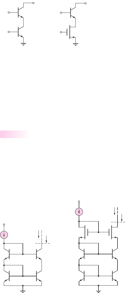
A bipolar multitransistor circuit previously studied is the Darlington pair configura-
tion. Figure 11.38(a) shows a modified Darlington pair configuration, in which the
bias current I
BIAS
, or some equivalent element, is used to control the quiescent
11.5.1
nea80644_ch11_753-850.qxd 6/19/09 4:37 AM Page 801 pmath DATA-DISK:Desktop Folder:18.6.09:MHDQ134-11:
802 Part 2 Analog Electronics
current in Q
1
. This Darlington pair circuit is used to boost the effective current gain
of bipolar transistors. There is no comparable configuration in FET circuits.
A potentially useful BiCMOS circuit is shown in Figure 11.38(b). Transistor Q
1
in the Darlington pair is replaced with a MOSFET. The advantages of this configura-
tion are an infinite input resistance, and a large transconductance due to the bipolar
transistor Q
2
.
To analyze the circuit, we consider the small-signal equivalent circuit shown in
Figure 11.39. We assume that
r
o
=∞
in both transistors.
The output signal current is
I
o
= g
m1
V
gs
+ g
m2
V
π
(11.111)
We see that
V
i
= V
gs
+ V
π
(11.112)
and
V
π
= g
m1
V
gs
r
π
(11.113)
Combining Equations (11.112) and (11.113) produces
V
gs
=
V
i
1 + g
m1
r
π
(11.114)
From Equation (11.111), the output current can now be written
I
o
= g
m1
V
gs
+ g
m2
(g
m1
r
π
)V
gs
= (g
m1
+ g
m2
g
m1
r
π
)V
gs
(11.115)
Substituting Equation (11.114) into (11.115), we obtain
I
o
=
g
m1
(1 + g
m2
r
π
)
(1 + g
m1
r
π
)
· V
i
= g
c
m
· V
i
(11.116)
where
g
c
m
is the composite transconductance. Since g
m2
of the bipolar transistor
is usually at least an order of magnitude greater than g
m1
of the MOSFET, the
composite transconductance is approximately an order of magnitude larger than that
of the MOSFET alone. We now have the advantages of a large transconductance and
an infinite input resistance.
A bipolar cascode circuit is shown in Figure 11.40(a); a corresponding BiCMOS
configuration is shown in Figure 11.40(b). The output resistance of the cascode
circuit is very high, as we saw in Chapter 10. Also, the cascode amplifier has a wider
(a) (b)
V
i
Q
1
Q
2
I
Bias
V
i
M
1
Q
2
I
Bias
Figure 11.38 (a) Bipolar Darlington pair configuration
and (b) BiCMOS Darlington pair configuration
V
p
r
p
g
m1
V
gs
g
m2
V
p
V
gs
+
–
+
–
V
i
I
o
+
–
Figure 11.39 Small-signal equivalent circuit,
BiCMOS Darlington pair configuration
nea80644_ch11_753-850.qxd 6/19/09 4:37 AM Page 802 pmath DATA-DISK:Desktop Folder:18.6.09:MHDQ134-11:
Chapter 11 Differential and Multistage Amplifiers 803
frequency bandwidth than the common-emitter circuit, since the input resistance
looking into the emitter of Q
2
is very low, thereby minimizing the Miller multiplica-
tion effect. This effect was observed in Chapter 7.
Again, the advantage of the BiCMOS circuit is the infinite input resistance of
M
1
. The equivalent resistance looking into the emitter of a bipolar transistor is much
less than the resistance looking into the source of a MOSFET; therefore, the fre-
quency response of a BiCMOS cascode circuit is superior to that of an all-MOSFET
cascode circuit.
Current Sources
In our previous discussions of constant-current sources, we mentioned that cascode
current sources increase the output resistance, as well as the stability of the bias
current. Figure 11.41 shows a bipolar cascode configuration in which the output
resistance is
R
o
∼
=
βr
o4
. The bias current in this circuit is much more stable against
variations in output voltage than the basic two-transistor current source.
A BiCMOS double cascode constant-current source is shown in Figure 11.42.
The small-signal equivalent circuit for determining output resistance is shown in
11.5.2
(a) (b)
v
o
Q
2
M
1
v
in
Bias
v
o
Q
2
Q
1
v
in
Bias
Figure 11.40 (a) Bipolar cascode configuration and (b) BiCMOS cascode configuration
R
o
I
O
I
REF
V
+
Q
4
Q
2
Q
3
Q
1
Figure 11.41 Bipolar cascode
constant-current source
R
o
I
O
I
REF
V
+
Q
4
Q
2
Q
3
M
6
M
5
Q
1
Figure 11.42 BiCMOS double
cascode constant-current source
nea80644_ch11_753-850.qxd 6/19/09 4:37 AM Page 803 pmath DATA-DISK:Desktop Folder:18.6.09:MHDQ134-11:
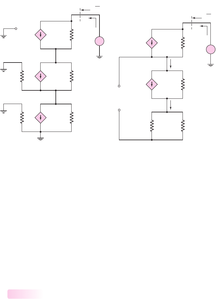
804 Part 2 Analog Electronics
Figure 11.43(a). The gate voltage to M
6
and the base voltages to Q
2
and Q
4
are
constants, equivalent to signal ground. Also, since
V
π2
= 0
, then
g
m6
V
π2
= 0
, and
the equivalent circuit can be rearranged as shown in Figure 11.43(b).
The output resistance of this circuit is extremely large. A detailed analysis shows
that the output resistance is given approximately by
R
o
∼
=
(g
m6
r
o6
)(βr
o4
)
(11.117)
The output resistance is increased by a factor (g
m
r
o6
) compared to the bipolar cascode
circuit in Figure 11.41. If a bipolar transistor were to be used in place of M
6
, then a re-
sistance
r
π6
would be connected across the terminals indicated by V
gs6
. This resistance
would effectively eliminate the multiplying constant (g
m6
r
o6
), and the output resis-
tance would be essentially the same as that of the circuit in Figure 11.41. The BiCMOS
circuit, then, increases the output resistance compared to an all-bipolar circuit.
BiCMOS Differential Amplifier
A basic BiCMOS differential amplifier, with a constant-current source bias and a
bipolar active load, is shown in Figure 11.44. Again, the primary advantages are
the infinite input resistance and the zero input bias current. One disadvantage of a
MOSFET input stage is a relatively high offset voltage compared to that of a bipolar
input circuit. Offset voltages occur when the differential-pair input transistors are
mismatched. In Chapter 14, we will examine the effect of offset voltages, as well as
nonzero bias currents, in op-amp circuits.
We will consider additional BiCMOS op-amp circuits in Chapter 13, when we
discuss the analysis and design of full op-amp circuits.
11.5.3
+
–
R
o
=
G
6
B
4
B
2
V
gs6
r
o6
r
o4
r
o2
V
p 4
V
p 2
r
p 2
r
p 4
g
m4
V
p 4
g
m2
V
p 2
g
m6
V
gs6
+
+
–
+
–
–
V
x
V
x
I
x
I
x
(a)
+
–
V
p 4
r
p 4
g
m4
V
p 4
g
m6
V
gs6
I
x
I
x
R
o
=
r
o6
r
o4
r
o2
V
gs6
+
–
V
1
+
–
–
+
V
x
V
x
I
x
I
x
(b)
Figure 11.43 (a) Equivalent circuit for determining output impedance of BiCMOS double
cascode current source and (b) rearranged equivalent circuit
nea80644_ch11_753-850.qxd 6/19/09 4:37 AM Page 804 pmath DATA-DISK:Desktop Folder:18.6.09:MHDQ134-11:
Chapter 11 Differential and Multistage Amplifiers 805
Test Your Understanding
TYU 11.16 Consider the BiCMOS Darlington pair in Figure 11.45. The NMOS
transistor parameters are
K
n
= 50 μ
A/V
2
,
V
TN
= 0.5
V, and
λ = 0
. The BJT para-
meters are
β = 150
,
V
BE
(
on
)
= 0.7
V, and
V
A
=∞
. Determine the small-signal pa-
rameters for each transistor, as well as the composite transconductance. (Ans.
g
m1
= 71.4 μ
A/V,
g
m2
= 2.865
mA/V,
r
π2
= 52.3
k
,
g
c
m
= 2.275
mA/V)
M
1
Q
2
I
Bias1
= 25 mA
I
Bias2
= 100 mA
C
Figure 11.45 Figure for Exercise TYU 11.16
V
+
V
–
I
Q
v
O
v
2
v
1
Q
1
Q
2
M
1
M
2
Figure 11.44 Basic BiCMOS differential amplifier
TYU 11.17
The reference current in each of the constant-current source circuits
shown in Figures 11.41 and 11.42 is
I
REF
= 0.5
mA. All bipolar transistor parameters
are
β = 150
and
V
A
= 80
V, and all MOSFET parameters are:
K
n
= 500 μA/V
2
,
V
TN
= 1
V, and
λ = 0.0125 V
−1
. Neglecting bipolar base currents, determine the
output resistance R
o
of each constant-current source. (Ans. For Figure 11.41,
R
o
∼
=
24 M
; for Figure 11.42,
R
o
= 3840 M
)
nea80644_ch11_753-850.qxd 6/19/09 4:37 AM Page 805 pmath DATA-DISK:Desktop Folder:18.6.09:MHDQ134-11:
806 Part 2 Analog Electronics
11.6 GAIN STAGE AND SIMPLE OUTPUT STAGE
Objective: • Analyze an example of a gain stage and output stage of
a multistage amplifier.
A diff-amp, including those previously discussed, is the input stage of virtually all
op-amps. The second op-amp stage, or gain stage, is often a Darlington pair config-
uration, and the third, or output, stage is normally an emitter follower.
Darlington Pair and Simple Emitter-Follower
Output
Figure 11.46 shows a BJT diff-amp with a three-transistor active load, a Darlington
pair connected to the diff-amp output, and a simple emitter-follower output stage.
11.6.1
The differential-pair transistors are biased with a Widlar current source at a bias
current I
Q
. We noted previously that, for the diff-amp dc currents to be balanced, we
must have
I
O
= I
B5
=
I
Q
β(1 +β)
(11.118)
From the figure, we see that
I
O
=
I
E6
(1 + β)
=
I
C7
β(1 +β)
(11.119)
I
Q
I
1
v
1
v
2
R
1
I
C7
I
B5
I
C1
I
C2
v
O2
v
O
v
O3
I
O
R
i
R
o
Q
9
Q
1
Q
2
Q
3
Q
5
Q
6
Q
8
Q
7
Q
4
Q
10
R
2
R
3
R
4
Q
11
V
+
V
–
V
–
V
–
Figure 11.46 BJT diff-amp with three-transistor active load, Darlington pair gain stage,
and simple emitter-follower output stage
nea80644_ch11_753-850.qxd 6/19/09 4:37 AM Page 806 pmath DATA-DISK:Desktop Folder:18.6.09:MHDQ134-11:
Chapter 11 Differential and Multistage Amplifiers 807
In order for
I
O
= I
B5
, we must require that
I
C7
= I
Q
. This means that the emitter
resistors of Q
10
and Q
11
should have the same value. Transistor Q
11
also acts as an
active load for the Darlington pair gain stage.
Transistor Q
8
and resistor R
4
form the simple emitter-follower output stage. The
emitter-follower amplifier minimizes loading effects because its output resistance is
small.
Ideally, when the diff-amp input is a pure common-mode signal, the output v
o
is
zero. The combination of Q
7
and Q
11
allows the dc level to shift. By slightly chang-
ing the bias current
I
C7
, we can vary voltages
V
EC7
and
V
CE11
such that
v
o
= 0
. The
small variation of
I
C7
required to achieve the necessary dc level shift will not signif-
icantly change the balance between I
O
and I
B5
. As we will see in later chapters, other
forms of level shifters could also be used.
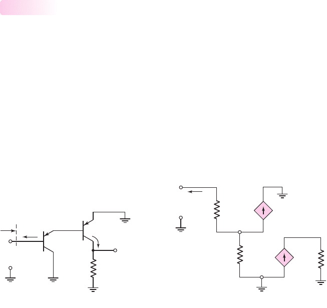
Input Impedance, Voltage Gain,
and Output Impedance
The input resistance of the Darlington pair determines the loading effect on the basic
diff-amp. In addition, the gain of the Darlington pair affects the overall gain of the
op-amp circuit, and the output resistance of the emitter follower determines any load-
ing effects on the output signal.
Figure 11.47(a) is the ac equivalent circuit of the Darlington pair, where R
L7
is
the effective resistance connected between the collector of Q
7
and signal ground.
Figure 11.47(b) shows the simple hybrid-π model of the Darlington pair. We see that
the equivalent circuits for Q
6
and Q
7
have been effectively turned upside down
compared to the transistors in Figure 11.47(a).
11.6.2
R
i
i
b6
i
c7
R
L7
v
o3
Q
6
Q
7
v
b6
–
+
I
b6
+
V
b6
R
L7
–
+
g
m7
V
p 7
g
m6
V
p 6
V
p 6
r
p 6
–
+
V
p 7
r
p 7
–
B
6
C
6
E
6
E
7
C
7
(a) (b)
Figure 11.47 (a) The ac equivalent circuit, Darlington pair, and (b) small-signal equivalent
circuit, Darlington pair
Writing a KVL equation around the B–E loop of Q
6
and Q
7
, we have
V
b6
= V
π6
+ V
π7
(11.120)
We can also write that
V
π6
= I
b6
r
π6
(11.121)
nea80644_ch11_753-850.qxd 6/19/09 4:37 AM Page 807 pmath DATA-DISK:Desktop Folder:18.6.09:MHDQ134-11: