Neamen D. Microelectronics: Circuit Analysis and Design
Подождите немного. Документ загружается.

818 Part 2 Analog Electronics
or
A
cm
=
−g
m
R
C
(1 + sR
o
C
o
)
1 +
R
B
r
π
(1 + sR
o
C
o
) +
2(1 + β)R
o
r
π
(11.139(b))
Equation (11.139(b)) shows that there is a zero in the common-mode gain. To
explain, capacitor C
o
is in parallel with R
o
, and it acts as a bypass capacitor. At very
low frequency, C
o
is effectively an open circuit and the common-mode signal “sees”
R
o
. As the frequency increases, the impedance of the capacitor decreases and R
o
is
effectively bypassed; hence, the zero in Equation (11.139(b)). The frequency ana-
lysis of an emitter bypass capacitor also showed the presence of a zero in the voltage
gain expression.
The common-mode gain frequency response is shown in Figure 11.52. The
frequency of the zero is
f
z
=
1
2π R
o
C
o
(11.140)
Since the output resistance R
o
of a constant-current source is normally large, a small
capacitance C
o
can result in a small f
z
. For frequencies greater than f
z
, the common-
mode gain increases at the rate of 6 dB/octave.
|A
CM
|
dB
f
Z
f
Figure 11.52 Frequency response of common-mode gain
Equation (11.139(b)) also shows that there is a pole associated with the
common-mode gain. Rearranging the terms in that equation, we see that the fre-
quency of the pole is
f
p
=
1
2π R
eq
C
o
(11.141)
where
R
eq
=
R
o
1 +
R
B
r
π
1 +
R
B
r
π
+
2(1 + β)R
o
r
π
(11.142)
The denominator of Equation (11.142) is very large, because of the term
(1 + β)R
o
.
This implies that R
eq
is small, which means that the frequency f
p
of the pole is very large.
The differential-mode gain is shown in Figure 11.53. The frequency response of
the common-mode rejection ratio is found by combining Figures 11.52 and 11.53,
and is shown in Figure 11.54.
nea80644_ch11_753-850.qxd 6/19/09 4:37 AM Page 818 pmath DATA-DISK:Desktop Folder:18.6.09:MHDQ134-11:
Chapter 11 Differential and Multistage Amplifiers 819
EXAMPLE 11.17
Objective: Determine the zero and pole frequencies in the common-mode gain.
Consider a diff-amp biased with a constant-current source. The output resistance
is
R
o
= 10 M
and the output capacitance is
C
o
= 1
pF. Assume the circuit and
transistor parameters are
R
B
= 0.5k
,
r
π
= 10 k
, and
β = 100
.
Solution: In the common-mode gain, the frequency of the zero is
f
z
=
1
2π R
o
C
o
=
1
2π(10 ×10
6
)(1 × 10
−12
)
⇒ 15.9 kHz
Also in the common-mode gain, the frequency of the pole is
f
P
= 1/(2π R
eq
C
o
)
where
R
eq
=
R
o
1 +
R
B
r
π
1 +
R
B
r
π
+
2(1 + β)R
o
r
π
=
(10 × 10
6
)
1 +
0.5
10
1 +
0.5
10
+
2(101)(10 × 10
6
)
10 × 10
3
or
R
eq
= 51.98
The frequency of the pole is therefore
f
P
=
1
2π(51.98)(1 ×10
−12
)
⇒ 3.06 GHz
Comment: The frequency of the zero in the common-mode gain is fairly low, while
the frequency of the pole is extremely large. The relatively low frequency of the zero
justifies neglecting the effect of
C
π
and
C
μ
. The CMRR frequency response is shown
in Figure 11.54, where f
z
is the zero frequency of the common-mode gain and f
H
is
the upper 3 dB frequency of the differential-mode gain.
EXERCISE PROBLEM
Ex 11.17: Repeat Example 11.17 for the case when the output capacitance of the
constant current source is
C
o
= 0.2
pF. (Ans.
f
z
= 79.6
kHz,
f
p
= 15.3
GHz)
|A
d
|
dB
f
H
Figure 11.53 Frequency response
of differential-mode gain
f
Z
f
H
f
– 6 dB/octave
–12 dB/octave
CMRR
dB
Figure 11.54 Frequency response
of common-mode rejection ratio
nea80644_ch11_753-850.qxd 6/19/09 4:37 AM Page 819 pmath DATA-DISK:Desktop Folder:18.6.09:MHDQ134-11:
820 Part 2 Analog Electronics
With Emitter-Degeneration Resistors
Figure 11.55 shows a bipolar diff-amp with two resistances R
E
connected in the
emitter portion of the circuit. One effect of including an emitter resistor is to reduce
the voltage gain, so the presence of these resistors is termed emitter degeneration.
In Chapter 7, we found that an emitter-follower circuit, which includes an emit-
ter resistance, is a wide-bandwidth amplifier. Therefore, one effect of resistors R
E
is an increase in the bandwidth of the differential amplifier. We rely on a computer
simulation to evaluate emitter degeneration effects.
11.8.3
V
+
V
–
R
C
R
C
R
E
R
E
v
O1
v
O2
Q
1
Q
2
v
1
v
2
V
e
I
Q
Figure 11.55 BJT differential amplifier
with emitter-degeneration resistors
10
3
10
4
10
5
10
6
10
7
1.0
10
100
R
E
= 0.125 kΩ
R
E
= 1 kΩ
R
E
= 0.50 kΩ
R
E
= 0.25 kΩ
f (Hz)
|A
d
|
Figure 11.56 PSpice results for frequency response
of diff-amp with emitter-degeneration
Figure 11.56 shows the frequency response of a one-sided differential-mode
gain, obtained from a PSpice analysis for four R
E
resistance values. The diff-amp
is biased at
I
Q
= 0.5
mA and the R
C
resistors are
R
C
= 30 k
. The transistor
capacitances are
C
π
= 34.6pF
and
C
μ
= 4.3
pF. As the emitter degeneration in-
creases, the differential-mode voltage gain decreases, but the bandwidth increases, as
previously indicated. The figure-of-merit for amplifiers, the gain-bandwidth product,
is approximately a constant for the results shown in Figure 11.56.
With Active Load
Figure 11.57 shows a bipolar diff-amp with an active load and a single input at v
1
.
The base and collector junctions of Q
3
are connected together, and a one-sided out-
put is taken at
v
O2
.
With the connection of Q
3
, the equivalent load resistance in the collector of Q
1
is on the order of
r
π
/(1 + β)
. This small resistance minimizes the Miller multiplica-
tion factor in Q
1
. Also, with the base of Q
2
at ground potential, one side of
C
μ2
is
grounded, and the Miller multiplication in Q
2
is zero. Therefore, we expect the band-
width of the diff-amp with an active load to be relatively wide. At high frequencies,
however, the effective impedance in the collector of Q
1
also includes the input
11.8.4
nea80644_ch11_753-850.qxd 6/19/09 4:37 AM Page 820 pmath DATA-DISK:Desktop Folder:18.6.09:MHDQ134-11:
Chapter 11 Differential and Multistage Amplifiers 821
V
+
V
–
Q
3
Q
1
Q
2
Q
4
v
O2
I
Q
v
1
v
2
= 0
Figure 11.57 BJT diff-amp with
active load and single-sided input
10
3
10
4
10
5
10
6
10
7
100
10
1000
2000
|A
d
|
f (Hz)
Figure 11.58 PSpice results for frequency response
of diff-amp with active load and single-sided input
capacitances of Q
3
and Q
4
. These additional capacitances also affect the frequency
response of the diff-amp, potentially narrowing the bandwidth.
Again, we rely on a computer analysis to determine the frequency characteristics
of the diff-amp with an active load. Figure 11.58 shows the results of the computer
simulation. The diff-amp is biased at
I
Q
= 0.5
mA, and the Early voltage of each
transistor is assumed to be 80 V. The transistor capacitances are
C
π
= 34.6pF
for
each transistor,
C
μ
= 3.8
pF in Q
1
and Q
2
, and
C
μ
= 7
pF and 5.5 pF in Q
3
and Q
4
,
respectively.
The low-frequency voltage gain is 1560 and the upper 3 dB frequency is 64 kHz.
The large gain is as expected for an active load amplifier, but the 3 dB frequency is
lower than expected. However, the gain–bandwidth product for the active load diff-
amp is approximately four times that of the diff-amp shown in Figure 11.55. The
increased gain–bandwidth product implies a reduced Miller multiplication factor in
the active load diff-amp, as predicted.
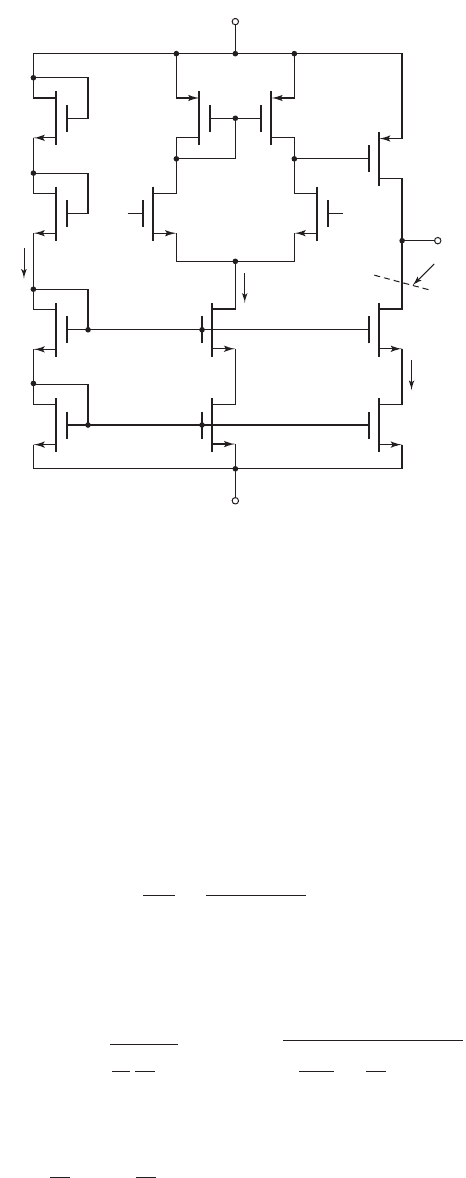
11.9 DESIGN APPLICATION: A CMOS DIFF-AMP
Objective: • Design a CMOS diff-amp with an output gain stage to
meet a set of specifications.
Specifications: Design a CMOS diff-amp with an output stage. The magnitude of
voltage gain of each stage is to be at least 600. Bias currents are to be
I
Q
= I
REF
=
100 μA
, and biasing of the circuit is to be
V
+
= 2.5
V and
V
−
=−2.5V
.
Design Approach: The circuit to be designed has the configuration shown in Fig-
ure 11.59. The diff-amp has NMOS amplifying transistors and a PMOS active load.
The diff-amp is biased with a cascode current source to provide a large output resis-
tance. The gain stage is a PMOS transistor in a common source configuration that
also has an active load.
nea80644_ch11_753-850.qxd 6/19/09 4:37 AM Page 821 pmath DATA-DISK:Desktop Folder:18.6.09:MHDQ134-11:
822 Part 2 Analog Electronics
– 2.5 V
+2.5 V
M
1
M
11
M
3
M
5
M
7
M
6
M
8
M
10
M
9
M
12
M
4
M
13
M
2
R
o12
I
D13
I
Q
= 100 mA
I
REF
v
O
v
o1
v
2
v
1
Figure 11.59 A CMOS diff-amp with an output stage for the design application
We will assume that several sets of transistors are matched. In particular, we will
assume that M
1
to M
4
, M
11
, and M
12
are matched; M
7
and M
8
are matched; M
5
and M
6
are matched; and M
9
and M
10
are matched.
Choices: Assume NMOS and PMOS transistors are available with parameters
V
TN
= 0.5V
,
V
TP
=−0.5V
,
k
n
= 80 μA/V
2
,
k
p
= 40 μA/V
2
, and
λ
n
= λ
p
=
0.01 V
−1
.
Solution (Differential Pair): The differential gain of the diff-amp is given by
A
d
= g
m
(r
o8
r
o10
)
We find
r
o8
= r
o10
=
1
λI
D
=
1
(0.01)(0.05)
= 2000 k
Then, for
A
d
= 600
, we have
600 = g
m
(20002000)
which yields
g
m
= 0.6
mA/V. Then
g
m
= 2
k
n
2
W
L
I
D
= 0.6 = 2
0.08
2
W
L
7
(0.05)
which yields
W
L
7
=
W
L
8
= 45
nea80644_ch11_753-850.qxd 6/19/09 4:37 AM Page 822 pmath DATA-DISK:Desktop Folder:18.6.09:MHDQ134-11:

Chapter 11 Differential and Multistage Amplifiers 823
We will also, somewhat arbitrarily, make the width-to-length ratios of all other tran-
sistors, except M
5
, M
6
, and M
13
, the same value of 45.
Solution (Current Source): We need to consider the two transistors M
5
and M
6
. The
gate-to-source voltages of M
1
and M
3
are found from
I
REF
= 100 =
80
2
(45)(V
GS1
−0.5)
2
which yields
V
GS1
= V
GS3
= 0.736
V. Since M
5
and M
6
are matched, we find
V
GS5
= V
GS6
=
2.5 − (−2.5) − 2(0.736)
2
= 1.76 V
The width-to-length ratios of M
5
and M
6
are found from
I
REF
= 100 =
80
2
W
L
5,6
(1.76 − 0.5)
2
which yields
W
L
5
=
W
L
6
= 1.57
Solution (Second Stage): The source-to-gate voltage applied to the common-
source transistor M
13
is equal to the source-to-drain voltage on M
10
which is the same
as the source-to-gate voltage of M
9
since the diff-amp is balanced. We find
I
D9
= 50 =
40
2
(45)(V
SG9
−0.5)
2
or
V
SG9
= V
SG13
= 0.736 V
The drain current in M
13
is
I
D13
= I
Q
= 100 μ
A because of the matched transistors
in the current source circuit. We now find
I
D13
I
D9
=
(W/L)
13
(W/L)
9
⇒
100
50
=
(W/L)
13
45
which yields
(W/L)
13
= 90
. The gain of the second stage is given by
A
2
=−g
m13
(r
o13
R
o12
)
We find
g
m13
= 2
k
p
2
W
L
13
I
D13
= 2
0.04
2
(90)(0.1) = 0.849 mA/V
and
r
o13
=
1
λI
D13
=
1
(0.01)(0.1)
= 1000 k
The output resistance R
o12
is given by
R
o12
= r
o12
+r
o11
(1 + g
m12
r
o12
)
nea80644_ch11_753-850.qxd 6/19/09 4:37 AM Page 823 pmath DATA-DISK:Desktop Folder:18.6.09:MHDQ134-11:

824 Part 2 Analog Electronics
We find
r
o11
= r
o12
=
1
λI
D12
=
1
(0.01)(0.1)
= 1000 k
and
g
m12
= 2
k
n
2
W
L
12
I
D12
= 2
0.08
2
(45)(0.1) = 0.849 mA/V
Then
R
o12
= 1000 +1000[1 +(0.849)(1000)] = 851,000 k
The second stage voltage gain is then
A
2
=−0.849(1000851,000) =−849
Solution (Overall Voltage Gain): Since there is no loading of the second stage on
the diff-amp circuit, the overall voltage gain is
A
v
= A
d
A
2
= (600)(−849) =−5.094 × 10
5
Comment: We may note that the amplifier we have just designed is an all MOSFET
circuit. The circuit contains no resistors. An all-transistor circuit is one of the advan-
tages of MOS transistors.
We may also note that a large voltage gain can be obtained from a circuit using
active loads.
11.10 SUMMARY
• The ideal transistor differential amplifier amplifies only the difference between
two input signals.
• The differential-mode input voltage is defined as the difference between the two
input signals and the common-mode input voltage is defined as the average of
the two input signals.
• When a differential input voltage is applied, one transistor of the differential pair
turns on more than the second transistor of the differential pair so that the cur-
rents become unbalanced, producing a signal output voltage.
• A common-mode output signal is generated when the output resistance of the
current source is finite rather than ideally infinite.
• The common-mode rejection ratio, CMRR, is defined in terms of decibels as
CMRR
dB
= 20 log
10
|
A
d
/A
cm
|
, where
A
d
and
A
cm
are the differential-mode volt-
age gain and common-mode voltage gain, respectively.
• Differential amplifiers are usually designed with active loads to increase the
differential-mode voltage gain.
• BiCMOS circuits may be designed to incorporate the best parameters and char-
acteristics of BJTs and MOSFETs in the same circuit.
• A BJT Darlington pair is typically used as a second stage in a BJT diff-amp. The
input impedance is large, which tends to minimize loading effects on the diff-amp,
and the effective current gain of the pair is the product of the individual gains.
• As an application, a CMOS diff-amp with an output gain stage was designed to
meet a set of specifications.
nea80644_ch11_753-850.qxd 6/19/09 4:34 PM Page 824 pmath DATA-DISK:Desktop Folder:19/6/2009:MHDQ134-11 Folder:MHDQ134-11

Chapter 11 Differential and Multistage Amplifiers 825
CHECKPOINT
After studying this chapter, the reader should have the ability to:
✓ Describe the mechanism by which a differential-mode signal and common-
mode signal are produced in a BJT diff-amp.
✓ Describe the dc transfer characteristics of a BJT diff-amp.
✓ Define common-mode rejection ratio.
✓ Describe the mechanism by which a differential-mode signal and common-
mode signal are produced in a MOSFET diff-amp.
✓ Describe the dc transfer characteristics of a MOSFET diff-amp.
✓ Design a MOSFET diff-amp with an active load to yield a specified differential-
mode voltage gain.
✓ Analyze a simplified BJT operational amplifier circuit.
✓ Design a simplified MOSFET operational amplifier circuit.
REVIEW QUESTIONS
1. Define differential-mode and common-mode input voltages.
2. Sketch the dc transfer characteristics of a BJT differential amplifier.
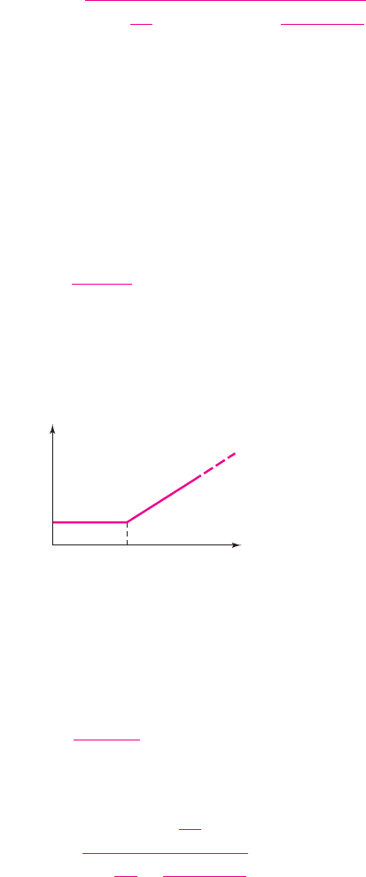
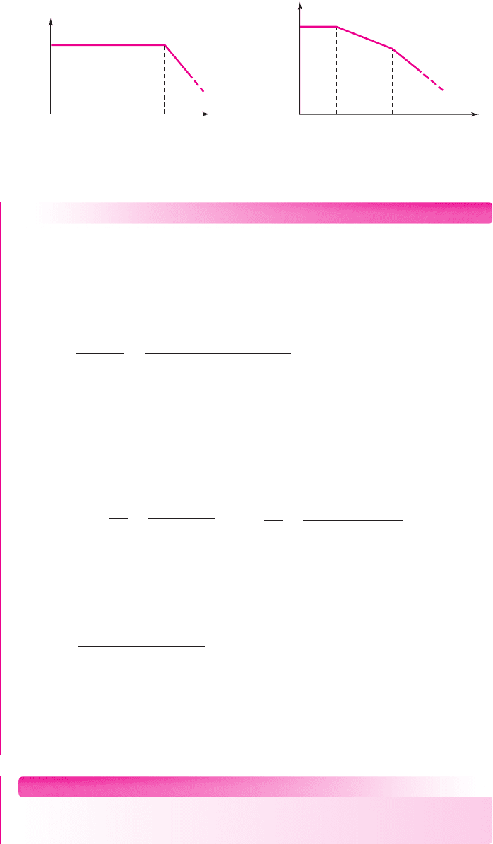
3. From the dc transfer characteristics, qualitatively define the linear region of
operation for a differential amplifier.
4. What is meant by matched transistors and why are matched transistors important
in the design of diff-amps?
5. Explain how a differential-mode output signal is generated.
6. Explain how a common-mode output signal is generated.
7. Define the common-mode rejection ratio, CMRR. What is the ideal value?
8. What design criteria will yield a large value of CMRR in an emitter-coupled pair?
9. Sketch the differential-mode and common-mode half-circuit models for an
emitter-coupled diff-amp.
10. Define differential-mode and common-mode input resistances.
11. Sketch the dc transfer characteristics of a MOSFET differential amplifier.
12. Sketch and describe the advantages of a MOSFET cascode current source used
with a MOSFET differential amplifier.
13. Sketch a simple MOSFET differential amplifier with an active load.
14. Explain the advantages of an active load.
15. Describe the loading effects of connecting a second stage to the output of a BJT
diff-amp.
16. Explain the frequency response of the differential-mode voltage gain.
17. Sketch a BJT Darlington pair circuit and explain the advantages.
18. Describe the three stages of a simple BJT operational amplifier.
PROBLEMS
Section 11.2 Basic BJT Differential Pair
11.1 (a) A differential-amplifier has a differential-mode gain of
A
d
= 250
and a
common-mode rejection ratio of
CMRR
dB
=∞
. A differential-mode input
signal of
v
d
= 1.5 sin ω t
mV is applied along with a common-mode input
signal of
v
cm
= 3 sin ωt
V. Assuming the common-mode gain is positive,
determine the output voltage. (b) Repeat part (a) if the common-mode
nea80644_ch11_753-850.qxd 6/19/09 4:34 PM Page 825 pmath DATA-DISK:Desktop Folder:19/6/2009:MHDQ134-11 Folder:MHDQ134-11
826 Part 2 Analog Electronics
I
C1
I
E
I
C2
+3 V
–3 V
R
C
R
E
v
O1
Q
1
v
1
v
2
Q
2
v
O2
R
C
+
–
+
–
Figure P11.3
rejection ratio is
CMRR
dB
= 80
dB. (c) Repeat part (a) if the common-
mode rejection ratio is
CMRR
dB
= 50
dB.
11.2 Consider the circuit shown in Figure P11.2. Assume
g
m
= 1.0
mA/V. As-
sume the input signal voltages are
v
1
= 0.7 +0.1 sin ω t
V and
v
2
=
0.7 − 0.1 sin ωt
V. (a) Determine the signal voltages (i)
v
o1
, (ii)
v
o2
, and
(iii)
v
o1
−v
o2
. (b) Using the results of part (a), determine the small-signal
voltage gains (i)
A
d1
= v
o1
/
(
v
1
−v
2
)
,
(ii)
A
d2
= v
o2
/
(
v
1
−v
2
)
, and
(iii)
A
d3
=
(
v
o1
−v
o2
)
/
(
v
1
−v
2
)
.
I
C2
I
C4
V
CE4
+
–
–5 V
+5 V
V
CE2
+
–
I
1
Q
1
Q
3
Q
4
Q
5
Q
2
R
1
=
8.5 kΩ
R
C
=
2 kΩ
R
C
=
2 kΩ
Figure P11.4
11.3 Consider the differential amplifier shown in Figure P11.3 with transistor
parameters
β = 150
,
V
BE
(
on
)
= 0.7
V, and
V
A
=∞
. (a) Design the circuit
such that the
Q
-point values are
I
C1
= I
C2
= 100 μ
A and
v
O1
=
v
O2
= 1.2
V for
v
1
= v
2
= 0
. (b) Draw the dc load line and plot the
Q
-point
for transistor
Q
2
. (c) What are the maximum and minimum values of the
common-mode input voltage?
v
1
v
2
v
O1
v
O2
R =
5 kΩ
R =
5 kΩ
V
+
= 5 V
g
m
v
2
g
m
v
1
+
–
+
–
Figure P11.2
11.4 The differential amplifier in Figure P11.4 is biased with a three-transistor cur-
rent source. The transistor parameters are:
β = 100
,
V
BE
(on) = 0.7
V, and
nea80644_ch11_753-850.qxd 6/19/09 4:37 AM Page 826 pmath DATA-DISK:Desktop Folder:18.6.09:MHDQ134-11:
Chapter 11 Differential and Multistage Amplifiers 827
V
+
= 15 V
V
–
= –15 V
R
C
R
C
Q
1
Q
2
Q
3
Q
4
v
1
v
2
I
C2
I
C1
v
O2
I
1
I
3
R
1
10 kΩ
10 kΩ
+
–
+
–
Figure P11.5
11.6 The diff-amp in Figure 11.3 of the text has parameters
V
+
=+5
V,
V
−
=−5V
,
R
C
= 8k
, and
I
Q
= 0.5
mA. The transistor parameters are
β = 120
,
V
BE
(on) = 0.7
V, and
V
A
=∞
. (a) Using Figure 11.3(a), deter-
mine the maximum common-mode input voltage
v
cm
that can be applied
such that the transistors Q
1
and Q
2
remain biased in the active region.
(b) Using Figure 11.3(b), determine the change in
v
C2
from its dc value if
v
d
= 18
mV. (c) Repeat part (b) if
v
d
= 10
mV.
D11.7 The diff-amp configuration shown in Figure P11.7 is biased at
±3
V. The
maximum power dissipation in the entire circuit is to be no more than
1.2 mW when
v
1
= v
2
= 0
. The available transistors have parameters:
β = 120
,
V
BE
(on) = 0.7
V, and
V
A
=∞
. Design the circuit to produce
the maximum possible differential-mode voltage gain, but such that the
common-mode input voltage can be within the range
−1 ≤ v
CM
≤ 1V
and
the transistors are still biased in the forward-active region. What is the value
of A
d
? What are the current and resistor values?
11.8 Consider the circuit in Figure P11.8, with transistor parameters:
β = 100
,
V
BE
(on) = 0.7
V, and
V
A
=∞
. (a) For
v
1
= v
2
= 0
, find I
C1
, I
C2
, I
E
, V
CE1
,
and V
CE2
. (b) Determine the maximum and minimum values of the
common-mode input voltage. (c) Calculate A
d
for a one-sided output at the
collector of Q
2
.
V
A
=∞
. (a) Determine I
1
, I
C2
, I
C4
,
V
CE2
, and
V
CE4
. (b) Determine a new
value of R
1
such that
V
CE4
= 2.5
V. What are the values of I
C4
, I
C2
, I
1
, and R
1
?
*D11.5 For the transistors in the circuit in Figure P11.5, the parameters are
β = 100
and
V
BE
(on) = 0.7
V. The Early voltage is
V
A
=∞
for Q
1
and Q
2
, and is
V
A
= 50
V for Q
3
and Q
4
. (a) Design resistor values such that
I
3
= 400 μA
and
V
CE1
= V
CE2
= 10
V. (b) Find A
d
, A
cm
, and CMRR
dB
for a one-sided
output at v
O2
. (c) Determine the differential- and common-mode input
resistances.
nea80644_ch11_753-850.qxd 6/19/09 4:37 AM Page 827 pmath DATA-DISK:Desktop Folder:18.6.09:MHDQ134-11: