Neamen D. Microelectronics: Circuit Analysis and Design
Подождите немного. Документ загружается.

828 Part 2 Analog Electronics
*11.9 The transistor parameters for the circuit in Figure P11.9 are:
β = 100
,
V
BE
(on) = 0.7
V, and
V
A
=∞
. (a) Determine R
E
such that
I
E
= 150 μA
.
(b) Find A
d
, A
cm
, and CMRR
dB
for a one-sided output at v
O2
. (c) Determine
the differential- and common-mode input resistances.
11.10 The bias voltages for the diff-amp shown in Figure P11.10 are
V
+
= 3
V
and
V
−
=−3
V. The transistor current gains are
β = 80
, the nominal value
of
V
BE
(
on
)
is 0.6 V, and
V
A
=∞
. (a) Design the circuit such that the qui-
escent collector currents are 50
μ
A and
v
C1
= v
C2
=−1.5
V for
v
1
= v
2
= 0
. (b) Determine
v
C1
and
v
C2
when (i)
v
1
= v
2
= 1
V and
(ii)
v
1
= 0.994
V,
v
2
= 1.006
V.
v
C1
v
C2
v
1
v
2
Q
1
Q
2
R
C
R
C
V
–
V
+
R
E
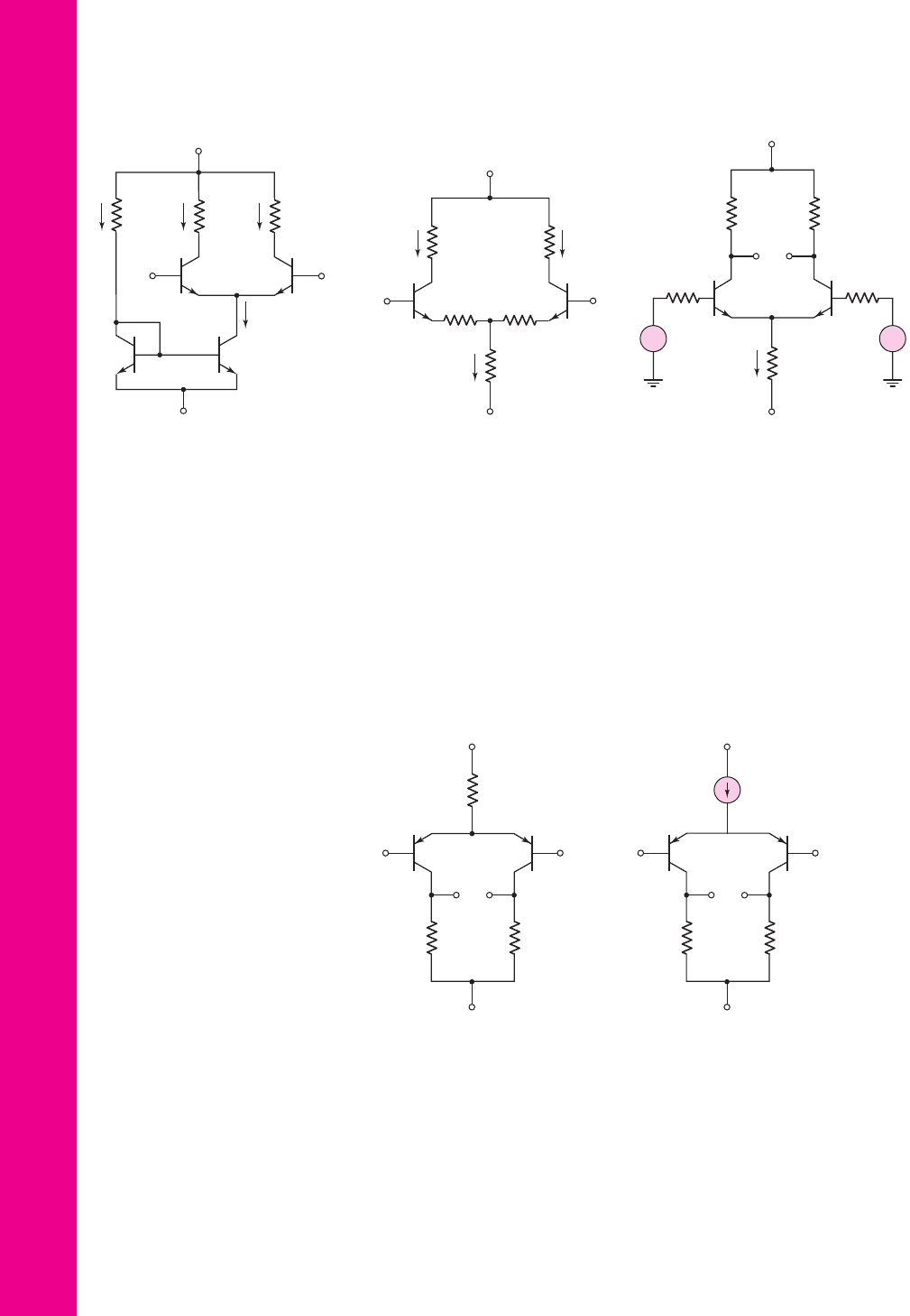
Figure P11.10
v
C1
v
C2
v
1
v
2
Q
1
Q
2
R
C
R
C
V
–
V
+
I
Q
Figure P11.11
I
C1
Q
1
Q
2
R
C
=
100 kΩ
R
C
=
100 kΩ
R
E
= 85 kΩ
I
C2
I
E
+5 V
–5 V
2 kΩ 2 kΩ
v
1
v
2
Figure P11.8
I
E
+10 V
–10 V
R
C
= 50 kΩ
R
E
R
B
= 0.5 kΩ R
B
= 0.5 kΩ
v
O1
v
O2
v
1
v
2
Q
1
Q
2
R
C
= 50 kΩ
+
–
+
–
Figure P11.9
11.11 Consider the circuit shown in Figure P11.11. The circuit and transistor
parameters are
V
+
=+3
V,
V
−
=−3
V,
R
C
= 360 k
,
I
Q
= 12 μA
,
β = 60
,
V
EB
(on) = 0.6
V, and
V
A
=∞
. The output resistance of the
current source is
R
o
= 4M
. (a) Determine the Q-points of the transistors
for
v
1
= v
2
= 0
. (b) Determine the differential- and common-mode voltage
gains for (i)
v
O
= v
C1
−v
C2
and (ii)
v
O
= v
C2
.
I
C4
I
1
I
C1
I
C2
V
+
V
–
R
C
R
C
R
1
Q
1
Q
2
Q
3
Q
4
v
1
v
2
Figure P11.7
nea80644_ch11_753-850.qxd 6/19/09 4:37 AM Page 828 pmath DATA-DISK:Desktop Folder:18.6.09:MHDQ134-11:
Chapter 11 Differential and Multistage Amplifiers 829
V
–
V
+
R
E
v
C1
v
C2
v
1
v
2
Q
1
Q
2
R
C
+
ΔR
2
R
C
–
ΔR
2
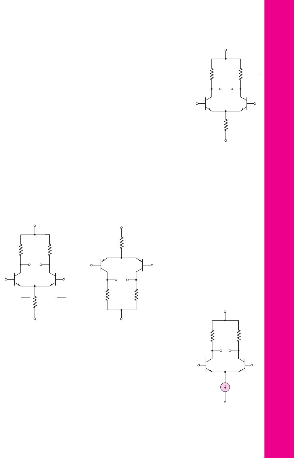
Figure P11.13
v
C1
v
E
v
C2
v
1
v
2
Q
1
Q
2
V
–
= –5 V
V
+
= 5 V
R
E
= 1.0 kΩ
R
C
=
1 kΩ
R
C
=
1 kΩ
Figure P11.15
V
–
V
+
R
E
v
C1
v
C2
v
1
v
2
Q
1
Q
2
R
C
R
C
g
m1
=
g
m
+
Δg
m
2
Δg
m
2
g
m2
=
g
m
–
Figure P11.14
11.12 The circuit and transistor parameters for the circuit shown in Figure P11.11
are
V
+
= 5
V,
V
−
=−5
V,
I
Q
= 0.2
mA,
β = 80
,
V
EB
(
on
)
= 0.6
V, and
V
A
=∞
. (a) Design the circuit such that the minimum common-mode
voltage is
v
cm
=−2.5
V. (b) Using the results of part (a), what is the
magnitude of the differential-mode gain,
A
d
=
|
(
v
C1
−v
C2
)
/
(
v
1
−v
2
)
|
?
(c) Determine
v
C1
and
v
C2
for
v
1
= 0.507
V and
v
2
= 0.493
V. (d) What
is the minimum output resistance of the current source such that
CMRR
dB
= 60
dB for a one-sided output.
11.13 Consider the differential amplifier shown in Figure P11.13 with mismatched
collector resistors. The circuit and transistor parameters are
V
+
= 5
V,
V
−
=−5
V,
β = 120
,
V
BE
(
on
)
= 0.7
V, and
V
A
=∞
. (a) For
R = 0
,
design the circuit such that
I
CQ1
= I
CQ2
= 120 μ
A and
v
C1
= v
C2
= 3
V
for
v
1
= v
2
= 0
. (b) Using the results of part (a), determine
|
A
d
|
for a two-
sided output. (c) For
R = 500
, determine
A
d
,
A
cm
, and
CMRR
dB
for
v
o
=
(
v
C1
−v
C2
)
.
11.14 Consider the differential amplifier shown in Figure P11.14 with mis-
matched transistors. The mismatched transistors result in mismatched
transconductances as shown. The circuit and transistor parameters are
V
+
=+10
V,
V
−
=−10
V,
R
C
= 50 k
,
R
E
= 75 k
,
β = 120
,
V
BE
(on) = 0.7
V, and
V
A
=∞
. Determine A
d
, A
cm
, and CMRR|
dB
for
g
m
/g
m
= 0.01
and for
v
O
= v
C1
−v
C2
. Assume
v
1
= v
2
= 0
in the
quiescent condition.
11.15 Consider the circuit in Figure P11.15. The transistor parameters are
β = 120
,
V
EB
(on) = 0.7
V, and
V
A
=∞
. Determine v
E
, v
C1
, and v
C2
for
(a)
v
1
= v
2
= 0
; (b)
v
1
= 0.5
V,
v
2
= 0
; and (c)
v
1
= 0
,
v
2
= 0.015
V.
11.16 (a) Design the circuit shown in Figure P11.16 such that
v
O
=
v
C1
−v
C2
= 1
V when
v
1
=−5
mV and
v
2
=+5
mV. The transistor pa-
rameters are
β = 180
,
V
BE
(on) = 0.7
V, and
V
A
=∞
. (b) Using the
results of part (a), determine the maximum common-mode input voltage.
11.17 Consider the differential amplifier in Figure P11.17 with parameters
V
+
= 5
V,
V
−
=−5
V, and
I
O
= 0.8
mA. Neglect base currents and
assume
V
A
=∞
for all transistors. The emitter currents can be written as
V
–
= –10 V
V
+
= 10 V
I
Q
= 2 mA
v
C1
v
C2
v
1
v
2
Q
1
Q
2
R
C
R
C
Figure P11.16
nea80644_ch11_753-850.qxd 6/19/09 4:37 AM Page 829 pmath DATA-DISK:Desktop Folder:18.6.09:MHDQ134-11:

830 Part 2 Analog Electronics
I
E1
= I
S1
e
V
BE1
/V
T
and
I
E2
= I
S2
e
V
BE2
/V
T
. (a) If
v
1
= v
2
= 0
and
I
S1
=
I
S2
= 3 ×10
−15
A, determine
(
v
O1
−v
O2
)
for (i)
R
C1
= R
C2
= 7.5k
and (ii)
R
C1
= 7.4k
,
R
C2
= 7.6k
. (b) Repeat part (a) for
I
S1
=
2.9 × 10
−15
A and
I
S2
= 3.1 ×10
−15
A.
11.18 For the diff-amp in Figure 11.2, determine the value of
v
d
= v
1
−v
2
that
produces (a)
i
C1
= 0.20I
Q
and (b)
i
C2
= 0.90I
Q
.
11.19 Consider the expanded dc transfer curves shown in Figure 11.6. Deter-
mine the maximum differential input voltage such that the actual curve is
within (a) 0.5 percent of the ideal linear extrapolation and (b) 1.5 percent
of the ideal extrapolation.
*D11.20 The diff-amp for the experimental system described in Example 11.4
needs to be redesigned. The range of the output voltage has increased to
−2 ≤ V
O
≤ 2V
while the differential-mode voltage gain is still
A
d
= 100
.
The common-mode input voltage has increased to
v
CM
= 3.5
V. The value
of CMRR needs to be increased to 80 dB.
*11.21 The transistor parameters for the circuit in Figure P11.9 are:
β = 120
,
V
BE
(on) = 0.7
V, and
V
A
=∞
. (a) Determine R
E
such that
I
E
= 0.25
mA.
(b) Assume the R
B
resistance connected to the base of Q
2
is zero while
the R
B
resistance connected to the base of Q
1
remains at
0.5k
.
(i) Determine the differential-mode voltage gain for a one-sided output at
v
O2
. (ii) Determine the common-mode voltage gain for a one-sided output
at v
O2
.
11.22 The circuit parameters of the diff-amp shown in Figure 11.2 are
V
+
= 3
V,
V
−
=−3
V, and
I
Q
= 0.25
mA. Base currents are negligible
and
V
A
=∞
for each transistor. (a) Design the circuit such that a differ-
ential-mode output voltage of
v
o
= v
C1
−v
C2
= 1.2
V is produced when
a differential-mode input voltage of
v
d
= v
1
−v
2
= 16
mV is applied. (b)
What is the maximum possible common-mode input voltage that can be
applied such that the input transistors remain biased in the forward-active
mode? (c) For a one-sided output, what is the value of
CMRR
dB
if the out-
put resistance of the current source is
R
o
= 4
M
?
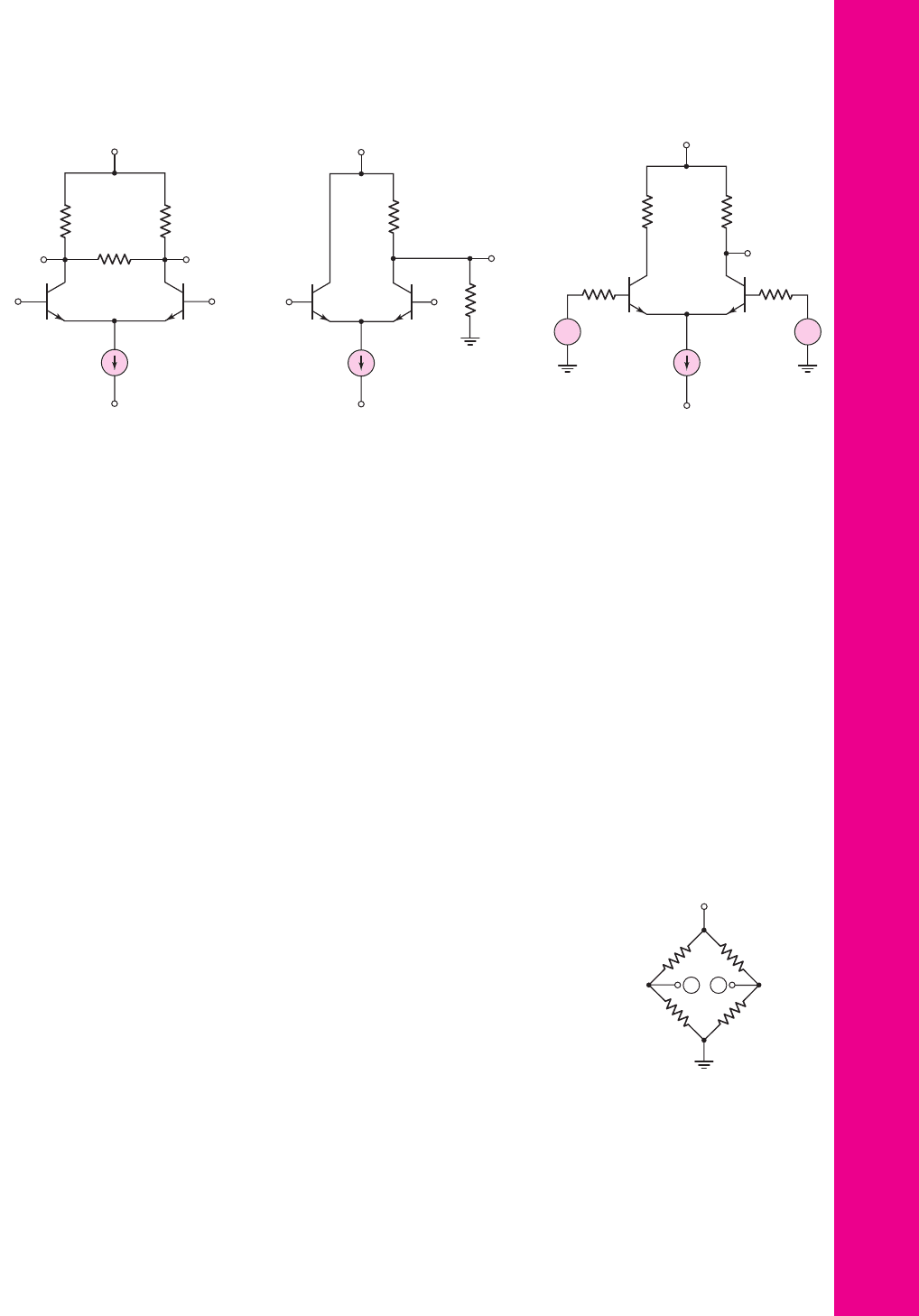
*11.23 Consider the circuit in Figure P11.23. Assume the Early voltage of Q
1
and Q
2
is
V
A
=∞
, and assume the current source I
Q
is ideal. Derive the
I
O
V
+
V
–
R
C1
v
O1
v
1
v
2
Q
1
Q
3
Q
4
Q
2
v
O2
R
C2
R
1
Figure P11.17
nea80644_ch11_753-850.qxd 6/19/09 4:37 AM Page 830 pmath DATA-DISK:Desktop Folder:18.6.09:MHDQ134-11:
Chapter 11 Differential and Multistage Amplifiers 831
R
C
R
C
R
L
Q
1
Q
2
v
1
v
2
v
O2
I
Q
v
O1
V
+
V
–
Figure P11.23
V
+
= +10 V
V
–
= –10 V
R
C
R
C
I
Q
= 0.2 mA
v
O
R
B
= 1 kΩR
B
= 1 kΩ
Q
1
v
1
v
2
Q
2
+
–
+
–
Figure P11.26
R
L
R
C
v
O
I
Q
Q
1
Q
2
v
1
v
2
V
+
V
–
Figure P11.24
expressions for the one-sided differential-mode gain
A
v1
= v
o1
/v
d
and
A
v2
= v
o2
/v
d
, and for the two-sided differential-mode gain
A
d
=
(v
o2
−v
o1
)/v
d
.
11.24 The Early voltage of transistors Q
1
and Q
2
in the circuit in Figure P11.24
is
V
A
=∞
. Assuming an ideal current source I
Q
, derive the expression for
the differential-mode gain
A
d
= v
o
/v
d
.
*11.25 Consider the small-signal equivalent circuit of the differential-pair config-
uration shown in Figure 11.9. Derive the expressions for the differential-
and common-mode voltage gains if the output is a two-sided output de-
fined as
V
o
= V
c2
− V
c1
.
*D11.26 Consider a BJT diff-amp with the configuration in Figure P11.26. The
signal sources have nonzero source resistances as shown. The transistor
parameters are:
β = 150
,
V
BE
(on) = 0.7
V, and
V
A
=∞
. The range of
the common-mode input voltage is to be
−3 ≤ v
CM
≤ 3
V and the CMRR
is to be 75 dB. (a) Design the diff-amp to produce the maximum possible
differential-mode voltage gain. (b) Design the current source to produce
the desired bias current and CMRR.
11.27 The bridge circuit in Figure P11.27 is a temperature transducer in which the
resistor
R
A
is a thermistor (a resistor whose resistance varies with tempera-
ture). The value of
δ
varies over the range of
−0.01 ≤ δ ≤ 0.01
as tem-
perature varies over a particular range. Assume the value of
R = 40
k
.
The bridge circuit is to be connected to the diff-amp in Figure 11.2. The
diff-amp circuit parameters are
V
+
= 5
V,
V
−
=−5
V,
I
Q
= 0.2
mA, and
R
C
= 15
k
. The transistor parameters are
β = 120
,
V
BE
(
on
)
= 0.7
V,
and
V
A
=∞
. Terminal A of the bridge circuit is connected to the base of
Q
1
and terminal B is connected to the base of
Q
2
. Determine the range of
output voltage
v
O2
as
δ
changes. [Hint: Make a Thevenin equivalent cir-
cuit at terminals A and B of the bridge circuit.]
11.28 A diff-amp is biased with a constant-current source
I
Q
= 0.25
mA that has
an output resistance of
R
o
= 8
M
. The bipolar transistor parameters are
β = 120
and
V
A
=∞
. Determine (a) the differential-mode input resis-
tance and (b) the common-mode input resistance.
A
RR
R
R
A
=
R(1 + d )
V
+
= 5 V
B
Figure P11.27
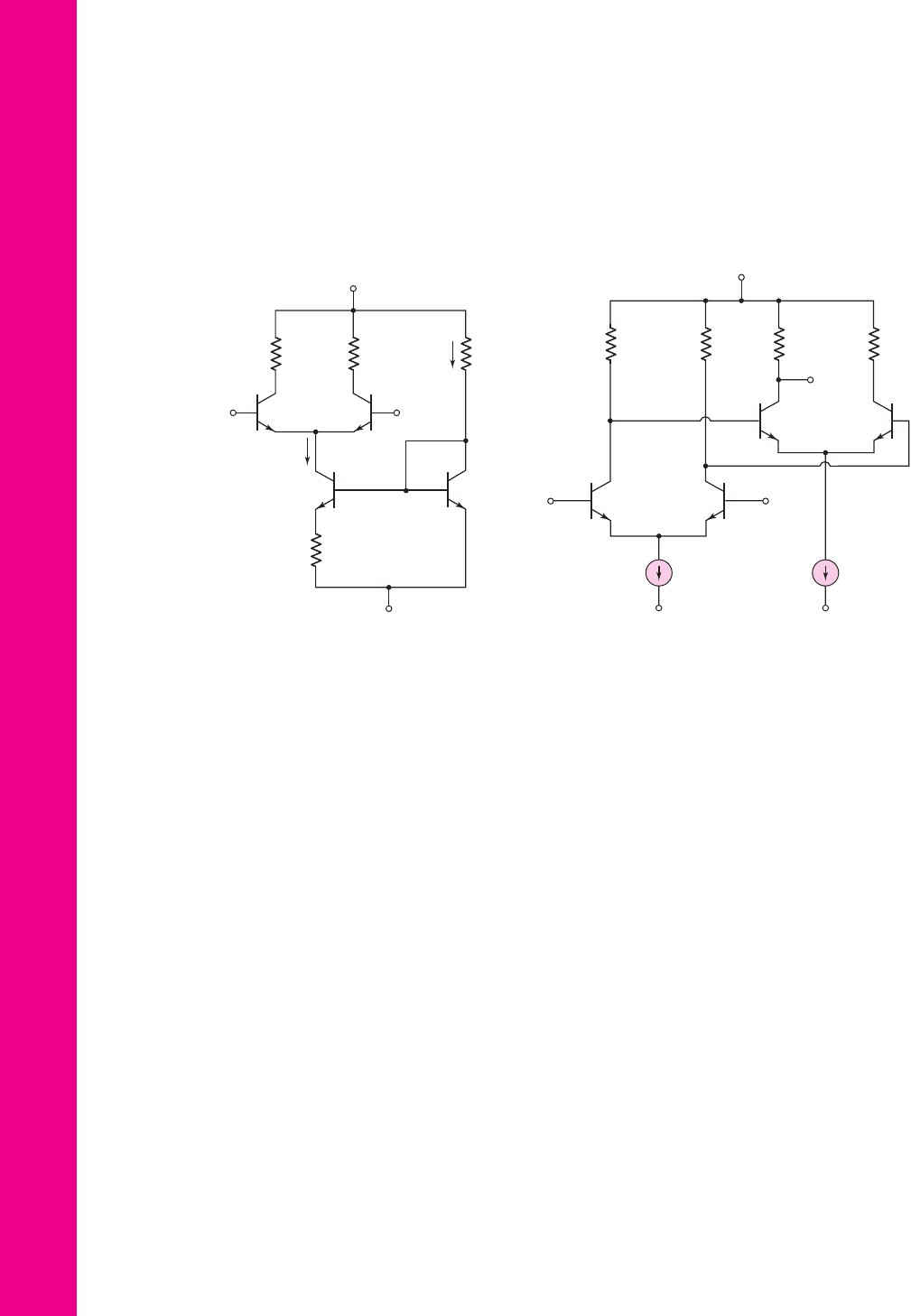
nea80644_ch11_753-850.qxd 6/19/09 4:37 AM Page 831 pmath DATA-DISK:Desktop Folder:18.6.09:MHDQ134-11:
832 Part 2 Analog Electronics
11.29 The transistor parameters for the circuit shown in Figure P11.29 are
β = 180
,
V
BE
(on) = 0.7
V (except for Q
4
),
V
A
=∞
for Q
1
and Q
2
, and
V
A
= 100
V for Q
3
and Q
4
. (a) Determine R
1
and R
2
such that
I
1
= 0.5
mA
and
I
Q
= 140 μA
. (b) Determine the common-mode input resistance.
(c) For
R
C
= 40 k
, determine the common-mode voltage gain.
R
C
R
C
I
1
I
Q
R
1
R
2
Q
1
Q
4
Q
3
v
1
v
2
Q
2
+10 V
–10 V
Figure P11.29
v
o3
v
1
v
2
v
o2
v
o1
I
Q1
I
Q2
v
out1
R
1
R
1
R
2
R
2
Q
3
Q
1
Q
2
Q
4
+10 V
–10 V –10 V
+–
Figure P11.30
D11.30 Figure P11.30 shows a two-stage cascade diff-amp with resistive loads. Power
supply voltages of
±10
V are available. Assume transistor parameters of:
β = 100
,
V
BE
(on) = 0.7
V, and
V
A
=∞
. Design the circuit such that the
two-sided differential-mode voltage gain is
A
d1
= (v
o2
−v
o1
)/
(v
1
−v
2
) = 20
for the first stage, and that the one-sided differential-mode
voltage gain is
A
d2
= v
o3
/(v
o2
−v
o1
) = 30
for the second stage. The cir-
cuit is to be designed such that the maximum differential-mode voltage
swing is obtained in each stage.
Section 11.3 Basic FET Differential Pair
11.31 For the differential amplifier in Figure P11.31 the parameters are
R
1
=50 k
and
R
D
= 24 k
. The transistor parameters are:
K
n
= 0.25
mA/V
2
,
λ = 0
,
and
V
TN
= 2
V. (a) Determine I
1
, I
Q
, I
D1
,
V
DS1
, and
V
DS4
when
v
1
= v
2
= 0
.
(b) Draw the dc load line and plot the Q-point for transistor M
2
. (c) What are
the maximum and minimum values of the common-mode input voltage?
11.32 The bias voltages in the diff-amp shown in Figure P11.31 are changed to
V
+
= 3
V and
V
−
=−3
V. The transistor parameters are
K
n1
= K
n2
=
100 μ
A/V
2
,
K
n3
= K
n4
= 200 μ
A/V
2
,
λ
1
= λ
2
= 0
,
λ
3
= λ
4
= 0.01
V
−1
and
V
TN
= 0.3
V (all transistors). (a) Design the circuit such that
V
DS1
= V
DS2
= 4
V and
I
D1
= I
D2
= 60 μ
A when
v
1
= v
2
=−1.15
V. (i)
What are the values of
I
Q
and
I
1
? (ii) What are the values of
R
D
and
R
1
?
(iii) What are the values of
V
GS1
and
V
GS4
? (b) Calculate the change in
I
Q
if
v
1
= v
2
=+1.15
V.
nea80644_ch11_753-850.qxd 6/19/09 4:37 AM Page 832 pmath DATA-DISK:Desktop Folder:18.6.09:MHDQ134-11:
Chapter 11 Differential and Multistage Amplifiers 833
11.33 The transistor parameters for the differential amplifier shown in
Figure P11.33 are
V
TN
= 0.5
V,
k
n
= 80 μA/V
2
,
W/L = 4
, and
λ = 0
.
(a) Find R
D
and I
Q
such that
I
D1
= I
D2
= 80 μA
and
v
O2
= 2V
when
v
1
= v
2
= 0
. (b) Draw the dc load line, and plot the Q-point for M
2
.
(c) What is the maximum common-mode input voltage?
11.34 The diff-amp in Figure P11.34 has parameters
V
+
= 3
V,
V
−
=−3
V, and
I
Q
= 0.18
mA. The transistor parameters are
V
TN
= 0.35
V,
k
n
=
100 μ
A/V
2
,
W
L = 4
, and
λ = 0
. (a) Using Figure P11.34(a), determine
R
D
such that the maximum value of the common-mode input voltage is
v
cm
(
max
)
= 2.25
V. The input transistors
M
1
and
M
2
must remain biased in
the saturation region. (b) Using Figure P11.34(b), determine the value of
v
D2
for (i)
v
d
= 0
, (ii)
v
d
=+120
mV, and (iii)
v
d
=−50
mV.
11.35 The bias voltages of the diff-amp shown in Figure P11.35 are
V
+
= 5
V and
V
−
=−5
V. The threshold voltage of each transistor is
V
TN
= 0.4
V and
R
D
I
D1
I
Q
v
O2
v
1
M
1
M
2
v
2
I
D2
R
D
V
+
= 10 V
V
–
= –10 V
Figure P11.33
V
+
= 10 V
V
–
= –10 V
M
1
v
1
v
2
M
2
M
4
M
3
I
D1
R
D
R
D
I
D2
I
Q
I
1
R
1
Figure P11.31
I
Q
I
D2
v
O2
v
O1
I
D1
I
1
V
+
V
–
v
1
R
1
R
D2
R
D1
M
1
M
2
M
4
M
3
v
2
Figure P11.35
R
D
I
Q
v
D2
v
cm
M
1
M
2
R
D
V
+
V
–
R
D
I
Q
v
D2
M
1
M
2
R
D
V
+
V
–
v
d
2
+
v
d
2
–
(a) (b)
Figure P11.34
nea80644_ch11_753-850.qxd 6/19/09 4:37 AM Page 833 pmath DATA-DISK:Desktop Folder:18.6.09:MHDQ134-11:
834 Part 2 Analog Electronics
R
D
R
D
v
2
v
D2
v
D1
v
1
M
1
M
2
R
S
I
S
V
+
V
–
Figure P11.38
R
D
R
D
v
2
v
D2
v
D1
v
1
M
1
M
2
I
Q
V
+
V
–
Figure P11.39
assume
λ = 0
. Let
K
n3
= K
n4
= 0.20
mA/V
2
. The drain currents can be
written as
I
D1
= K
n1
(
V
GS1
− V
TN
)
2
and
I
D2
= K
n2
(
V
GS2
− V
TN
)
2
.
(a) Design the circuit such that
I
Q
= 0.25
mA when
v
1
= v
2
= 0
. (b) If
v
1
= v
2
= 0
and
K
n1
= K
n2
= 0.120
mA/V
2
, find
v
O1
−v
O2
when (i)
R
D1
=
R
D2
= 15
k
and (ii)
R
D1
= 14.5
k
,
R
D2
= 15.5
k
. (c) Repeat part (b)
for
K
n1
= 0.125
mA/V
2
and
K
n2
= 0.115
mA/V
2
.
11.36 The circuit parameters of the diff-amp shown in Figure 11.19 are
V
+
= 3
V,
V
−
=−3
V, and
I
Q
= 0.15
mA. The transistor parameters are
K
n
= 0.2
mA/V
2
,
V
TN
= 0.4
V, and
λ = 0
. Determine the value of
v
d
=
v
G1
−v
G2
that produces (a)
i
D1
= 0.2I
Q
, (b)
i
D2
= 0.8I
Q
, and (c)
i
D1
= I
Q
.
11.37 Consider the normalized dc transfer characteristics of a MOSFET diff-amp
shown in Figure 11.21. Assume that
K
n
= 0.20
mA/V
2
and
I
Q
= 0.10
mA.
Determine the maximum differential input voltage such that the actual
curve of
i
D1
/I
Q
is within (a) 0.5 percent of the ideal linear extrapolation and
(b) 1.5 percent of the ideal linear extrapolation.
11.38 The parameters of the diff-amp circuit shown in Figure P11.38 are
V
+
= 9
V,
V
−
=−9V
,
R
D
= 510 k
, and
R
S
= 390 k
. The transistor parameters
are
V
TP
=−0.8V
,
K
p
= 50 μA/V
2
, and
λ = 0
. Determine v
D1
and v
D2
for
(a)
v
1
= v
2
= 1
V and (b)
v
1
= 1.050
V,
v
2
= 0.950
V.
11.39 Consider the circuit shown in Figure P11.39. The circuit and transistor
parameters are
V
+
=+3
V,
V
−
=−3
V,
R
D
= 360 k
,
I
Q
= 12 μA
,
V
TP
=−0.4
V,
K
p
= 30 μ
A/V
2
, and
λ = 0
. The output resistance of the
current source is
R
o
= 4M
. (a) Determine the Q-points of the transistors
for
v
1
= v
2
= 0
. (b) Determine the differential- and common-mode voltage
gains for (i)
v
O
= v
D1
−v
D2
and (ii)
v
O
= v
D2
.
11.40 The circuit and transistor parameters for the circuit shown in Figure P11.39
are
V
+
= 5
V,
V
−
=−5
V,
I
Q
= 0.15
mA,
R
D
= 30
k
,
V
TP
=−0.5
V,
K
p
= 0.12
mA/V
2
, and
λ = 0
. The output resistance of the current source is
R
o
= 4
M
. (a) Determine
v
D1
−v
D2
for (i)
v
1
=+0.05
V,
v
2
=−0.05
V
and (ii)
v
1
=+0.10
V,
v
2
=−0.10
V. (b) Determine the change in
v
D2
as
the inputs change (i) from
v
1
= v
2
= 0
to
v
1
= 0.10
V and
v
2
=−0.10
V,
and (ii) from
v
1
= v
2
= 0
to
v
1
= 1.10
V and
v
2
= 0.90
V.
nea80644_ch11_753-850.qxd 6/19/09 4:37 AM Page 834 pmath DATA-DISK:Desktop Folder:18.6.09:MHDQ134-11:
Chapter 11 Differential and Multistage Amplifiers 835
v
2
v
D2
v
D1
v
1
M
1
M
2
V
+
= 5 V
V
–
= –5 V
R
S
=
2 kΩ
R
D
=
1 kΩ
R
D
=
1 kΩ
Figure P11.43
R
S
v
D2
v
D1
v
2
v
1
M
1
M
2
V
+
V
–
R
D
R
D
g
m1
=
g
m
+
Δg
m
2
Δg
m
2
g
m2
=
g
m
–
Figure P11.42
R
S
v
D2
v
D1
v
2
v
1
M
1
M
2
V
+
V
–
R
D
+
ΔR
2
R
D
–
ΔR
2
Figure P11.41
11.41 Consider the differential amplifier shown in Figure P11.41 with mis-
matched drain resistors. The circuit and transistor parameters are
V
+
=
+10
V,
V
−
=−10
V,
R
D
= 50 k
,
R
S
= 75 k
,
V
TN
= 1
V,
K
n
=
0.15 mA/V
2
, and
λ = 0
. Determine A
d
, A
cm
, and CMRR|
dB
for
R =
500
and for
v
O
= v
D1
−v
D2
. Assume
v
1
= v
2
= 0
in the quiescent
condition.
11.42 Consider the differential amplifier shown in Figure P11.42 with mis-
matched transistors. The mismatched transistors result in mismatched
transconductances as shown. The circuit and transistor parameters are
V
+
=+10
V,
V
−
=−10
V,
R
D
= 50 k
,
R
S
= 75 k
,
V
TN
= 1
V,
K
n
= 0.15
mA/V
2
, and
λ = 0
. Determine A
d
, A
cm
, and CMRR|
dB
for
g
m
/g
m
= 0.01
and for
v
O
= v
D1
−v
D2
. Assume
v
1
= v
2
= 0
in the
quiescent condition.
11.43 Consider the circuit in Figure P11.43. The transistor parameters are
K
p
= 1.2
mA/V
2
,
V
TP
=−0.6
V, and
λ = 0
. Determine
v
S
,
v
D1
, and
v
D2
for (a)
v
1
= v
2
= 0
; (b)
v
1
= v
2
= 1
V; (c)
v
1
=−0.1
V,
v
2
= 0.1
V; and
(d)
v
1
= 0.9
V,
v
2
= 1.1
V.
D11.44 (a) Design the circuit shown in Figure P11.44 such that
v
O
= v
D1
−v
D2
=
1V
when
v
1
=−50 mV
and
v
2
=+50 mV
. The transistor parameters are
V
TN
= 0.8V
,
K
n
= 0.4mA/V
2
, and
λ = 0
. (b) Using the results of
part (a), determine the maximum common-mode input voltage.
*D11.45 The Hall effect experimental arrangement was described in Example 11.4.
The required diff-amp is to be designed in the circuit configuration in Fig-
ure P11.35. The transistor parameters are
V
TN
= 0.8
V,
k
n
= 80 μA/V
2
,
λ
1
= λ
2
= 0
, and
λ
3
= λ
4
= 0.01 V
−1
. If the CMRR requirement cannot
be met, a more sophisticated current source may have to be designed.
*11.46 Consider the diff-amp in Figure P11.46. The transistor parameters are:
K
n1
= K
n2
= 50 μA/V
2
,
λ
1
= λ
2
= 0.02 V
−1
, and
V
TN1
= V
TN2
= 1V
.
(a) Determine
I
S
, I
D1
, I
D2
, and
v
O2
for
v
1
= v
2
= 0
. (b) Using the small-
signal equivalent circuit, determine the differential-mode voltage gain
A
d
=
v
o2
/v
d
, the common-mode voltage gain
A
cm
= v
o2
/v
cm
, and the CMRR
dB
.
nea80644_ch11_753-850.qxd 6/19/09 4:37 AM Page 835 pmath DATA-DISK:Desktop Folder:18.6.09:MHDQ134-11:
836 Part 2 Analog Electronics
11.47 Consider the circuit shown in Figure P11.47. Assume that
λ = 0
for M
1
and M
2
. Also assume an ideal current source I
Q
. Derive the expression for
the one-sided differential mode gains
A
d1
= v
o1
/v
d
and
A
d2
= v
o2
/v
d
,
and the two-sided differential-mode gain
A
d
= (v
o2
−v
o1
)/v
d
.
I
Q
=
2 mA
v
D2
v
D1
v
2
v
1
M
1
M
2
V
+
= 10 V
V
–
= –10 V
R
D
R
D
Figure P11.44
v
2
I
D1
I
S
v
O2
v
1
M
1
M
2
I
D2
R
S
= 20 kΩ
R
D
= 25 kΩ
R
D
= 25 kΩ
V
+
= 5 V
V
–
= –5 V
Figure P11.46
11.48 Consider the diff-amp shown in Figure P11.48. Assume
λ
1
= λ
2
= 0
and
assume the current source has an output resistance of
R
o
. (a) Derive the
expression for the differential-mode voltage gain
A
d
= v
O
/v
d
where
v
d
= v
1
−v
2
. (b) Derive the expression for the common-mode voltage
gain
A
cm
= v
O
/v
cm
where
v
cm
=
(
v
1
+v
2
)
/2
.
11.49 The bias voltages of the diff-amp circuit shown in Figure 11.19 are
V
+
= 5
V and
V
−
=−5
V, and the bias current is
I
Q
= 0.2
mA. The tran-
sistor parameters are
V
TN
= 0.4
V,
K
n
= 0.15
mA/V
2
, and
λ = 0
. (a) De-
sign the circuit such that a differential-mode output voltage of
v
O
= 0.5
Vis
V
+
V
–
R
D
R
D
R
L
I
Q
v
O1
v
1
M
1
M
2
v
2
v
O2
Figure P11.47
V
+
V
–
R
D
R
L
v
O
I
Q
v
1
M
1
M
2
v
2
Figure P11.48
nea80644_ch11_753-850.qxd 6/19/09 4:38 AM Page 836 pmath DATA-DISK:Desktop Folder:18.6.09:MHDQ134-11:
Chapter 11 Differential and Multistage Amplifiers 837
produced when a differential-mode input voltage of
v
d
= v
1
−v
2
= 100
mV
is applied. (b) Using the results of part (a), determine the maximum possible
common-mode input voltage that can be applied such that the transistors re-
main biased in the saturation region.
11.50 Consider the small-signal equivalent circuit in Figure 11.23. Assume the
output is a two-sided output defined as
V
o
= V
d2
− V
d1
, where V
d2
and V
d1
are the signal voltages at the drains of M
2
and M
1
, respectively. Derive
expressions for the differential- and common-mode voltage gains.
11.51 Consider the MOSFET diff-amp with the configuration in Figure
P11.33. The circuit parameters are
V
+
= 3
V,
V
−
=−3
V, and
I
Q
= 0.2
mA. The transistor parameters are
V
TN
= 0.4
V,
k
n
= 100 μ
A/V
2
,
W/L = 10
, and
λ = 0
. The range of the common-
mode input voltage is to be
−1.5 ≤ v
cm
≤+1.5
V, and the common-
mode rejection ratio is to be
CMRR
dB
= 50
dB. (a) Design the diff-amp
to produce the maximum possible differential-mode voltage gain. (b)
Design an all MOSFET current source to produce the desired bias cur-
rent and CMRR. The minimum
W/L
ratio of any transistor is to be 0.8,
and assume
λ = 0.02 V
−1
for all transistors in the current source circuit.
11.52 Consider the bridge circuit and diff-amp described in Problem 11.27. The
BJT diff-amp is to be replaced with a MOSFET diff-amp as shown in Fig-
ure 11.19. The transistor parameters are
V
TN
= 0.4
V,
K
n
= 1
mA/V
2
,
and
λ = 0
. The bias voltages of the MOSFET diff-amp are
V
+
= 5
V and
V
−
=−5
V, and the reference current is
I
Q
= 0.2
mA. Let
R
D
= 20
k
.
Terminal A of the bridge circuit is to be connected to the gate of
M
1
and
terminal B is to be connected to the gate of
M
2
. (a) Determine the range of
output voltage
v
O
as
δ
changes. (b) Explain the advantages and disadvan-
tages of this circuit configuration compared to that in Problem 11.27.
*D11.53 Figure P11.53 shows a two-stage cascade diff-amp with resistive loads.
Power supply voltages of
±10
V are available. Assume transistor param-
eters of
V
TN
= 1V
,
k
n
= 60 μA/V
2
, and
λ = 0
. Design the circuit such
R
1
R
1
R
2
R
2
+10 V
–10 V
I
Q1
–10 V
I
Q2
v
2
v
o3
v
o2
v
o1
v
1
M
1
M
2
M
3
M
4
–+
v
out1
Figure P11.53
nea80644_ch11_753-850.qxd 6/19/09 4:38 AM Page 837 pmath DATA-DISK:Desktop Folder:18.6.09:MHDQ134-11: