Neamen D. Microelectronics: Circuit Analysis and Design
Подождите немного. Документ загружается.

838 Part 2 Analog Electronics
that the two-sided differential-mode voltage gain is
A
d1
= (v
o2
−v
o1
)/
(v
1
−v
2
) = 20
for the first stage, and that the one-sided differential-mode
voltage gain is
A
d2
= v
o3
/(v
o2
−v
o1
) = 30
for the second stage. The cir-
cuit is to be designed such that the maximum differential-mode voltage
swing is obtained in each stage.
*11.54 Figure P11.54 shows a matched JFET differential pair biased with a cur-
rent source I
Q
. (a) Starting with
i
D
= I
DSS
1 −
v
GS
V
P
2
show that
i
D1
I
Q
=
1
2
+
1
−2V
P
v
d
2
I
DSS
I
Q
−
I
DSS
I
Q
2
v
d
V
P
2
and
i
D2
I
Q
=
1
2
−
1
−2V
P
v
d
2
I
DSS
I
Q
−
I
DSS
I
Q
2
v
d
V
P
2
(b) Show that the I
Q
bias current is switched entirely to one transistor or
the other when
|
v
d
|
=
|
V
P
|
I
Q
I
DSS
(c) Show that the maximum forward transconductance is given by
g
f
(max) =
di
D1
dv
d
v
d
=0
=
1
−V
P
I
Q
· I
DSS
2
i
D1
v
G1
v
G2
Q
1
Q
2
V
–
i
D2
I
Q
Figure P11.54
11.55 A JFET differential amplifier is shown in Figure P11.55. The transistor
parameters are:
V
P
=−4V
,
I
DSS
= 2
mA, and
λ = 0
. (a) Find R
D
and
I
Q
such that
I
D1
= I
D2
= 0.5
mA and
v
o2
= 7
V when
v
1
= v
2
= 0
.
V
+
= 10 V
V
–
= –10 V
I
D1
Q
1
Q
2
I
D2
v
1
v
2
v
O
I
Q
R
D
R
D
Figure P11.55
nea80644_ch11_753-850.qxd 6/19/09 4:38 AM Page 838 pmath DATA-DISK:Desktop Folder:18.6.09:MHDQ134-11:
Chapter 11 Differential and Multistage Amplifiers 839
V
+
= 5 V
V
–
= –5 V
R
D
=
25 kΩ
R
D
=
25 kΩ
R
S
= 20 kΩ
I
D1
I
S
I
D2
Q
1
Q
2
v
1
v
2
v
O2
Figure P11.56
V
+
V
–
R
D
R
D
I
Q
R
L
v
O1
v
1
Q
1
Q
2
v
2
v
O2
Figure P11.57
(b) Calculate the maximum forward transconductance. (c) Determine
the one-sided differential-mode voltage gain
A
d
= v
o
/v
d
.
*11.56 Consider the JFET diff-amp shown in Figure P11.56. The transistor
parameters are:
I
DSS
= 0.8
mA,
λ = 0
, and
V
P
=−2V.
(a) Determine I
S
,
I
D1
, I
D2
, and
v
o2
for
v
1
= v
2
= 0
. (b) Using the small-signal equivalent cir-
cuit, determine the differential-mode voltage gain
A
d
= v
o2
/v
d
, the com-
mon-mode voltage gain
A
cm
= v
o
/v
cm
, and the CMRR
dB
.
*11.57 Consider the circuit in Figure P11.57. Assume that
λ = 0
for the transis-
tors, and assume an ideal current source I
Q
. Derive the expressions for the
one-sided differential-mode gains
A
d1
= v
o1
/v
d
and
A
d2
= v
o2
/v
d
, and
for the two-sided differential-mode gain
A
d
= (v
o2
−v
o1
)/v
d
.
Section 11.4 Differential Amplifier with Active Load
11.58 The circuit parameters for the diff-amp shown in Figure 11.30 are
V
+
= 3.3
V,
V
−
=−3.3
V, and
I
Q
= 0.4
mA. The transistor parameters are
β = 120
,
V
A1
= V
A2
= 120
V,
V
A3
= V
A4
= 80
V, and
V
A5
=∞
. (a) De-
termine the open-circuit differential-mode voltage gain. (b) What is the output
resistance of the diff-amp? (c) Find the value of load resistance
R
L
that
reduces the differential-mode gain to 75 percent of the open-circuit value.
D11.59 Design a differential amplifier with the configuration shown in Figure 11.28
incorporating a basic two-transistor current source to establish I
Q
. The bias
voltages are to be
V
+
=+5
V and
V
−
=−5V
, the bias current is to be
I
Q
= 250 μA
, and the available transistors have parameters
β = 180
,
V
BE
(on) = V
EB
(on) = 0.7
V,
V
AN
= 150
V, and
V
AP
= 100
V. (a) Show
the complete circuit. (b) What is the open-circuit differential-mode voltage
gain. (c) Determine the differential-mode input resistance and the output
resistance. (d) Determine the common-mode input voltage range.
11.60 The differential amplifier shown in Figure P11.60 has a pair of pnp bipo-
lars as input devices and a pair of npn bipolars connected as an active load.
nea80644_ch11_753-850.qxd 6/19/09 4:38 AM Page 839 pmath DATA-DISK:Desktop Folder:18.6.09:MHDQ134-11:

840 Part 2 Analog Electronics
The circuit bias is
I
Q
= 0.2
mA, and the transistor parameters are
β = 100
and
V
A
= 100
V. (a) Determine I
0
such that the dc currents in the
diff-amp are balanced. (b) Find the open-circuit differential-mode voltage
gain. (c) Determine the differential-mode voltage gain if a load resistance
R
L
= 250 k
is connected to the output.
11.61 The bias voltages for the diff-amp shown in Figure 11.30 are
V
+
= 5
V
and
V
−
=−5
V. A load resistance of
R
L
= 250
k
is capacitively cou-
pled to the output. The transistor parameters are
β = 120
,
V
A1
= V
A2
= 90
V, and
V
A3
= V
A4
= 60
V. (a) Determine the bias current
I
Q
that will produce a differential-mode voltage gain of
A
d
= 1000
. (b) If
V
EB
(
on
)
= 0.6
V, what is the maximum common-mode voltage that can
be applied such that all transistors are biased in the forward-active mode?
11.62 Consider the diff-amp shown in Figure P11.62. The circuit parameters are
V
+
= 3
V,
V
−
=−3
V, and
I
Q
= 0.4
mA. The npn transistor parameters
are
β
npn
= 180
,
V
BE
(
on
)
= 0.7
V, and
V
AN
= 120
V, and the pnp transis-
tor parameters are
β
pnp
= 120
,
V
EB
(
on
)
= 0.7
V, and
V
AP
= 80
V. (a)
Sketch the small-signal equivalent circuit for the diff-amp assuming an
ideal differential-mode input signal. (b) Determine the one-sided differen-
tial-mode gain
A
d1
= v
O1
/v
d
. (c) Determine the one-sided differential-
mode gain
A
d2
= v
O2
/v
d
. (d) Find the two-sided differential-mode gain
A
d3
=
(
v
O2
−v
O1
)
/v
d
.
11.63 Consider the MOSFET diff-amp shown in Figure P11.63. The bias voltages
are
V
+
= 3
V and
V
−
=−3
V. The current source is
I
Q
= 200 μ
A and has
an output resistance of
R
o
= 2
M
. The transistor parameters are
V
TN
= 0.4
V,
V
TP
=−0.4
V,
K
n
= K
p
= 0.5
mA/V
2
,
λ
2
= 0.02
V, V
−1
,
λ
4
= 0.03 V
−1
and
λ
1
= λ
3
= 0
. (a) Determine the voltage gain
A = v
o
/v
d
for
v
1
= v
d
and
v
2
= 0
. (b) Determine the voltage gain
A = v
o
/v
d
for
v
1
= 0
and
v
2
=−v
d
. (c) Determine the voltage gain
A = v
o
/v
d
for
v
1
= v
d
/2
and
v
2
=−v
d
/2
.
11.64 The differential amplifier in Figure P11.64 has a pair of PMOS transistors
as input devices and a pair of NMOS transistors connected as an active
load. The circuit is biased with
I
Q
= 0.2
mA, and the transistor parame-
ters are:
K
n
= K
p
= 0.1mA/V
2
,
λ
n
= 0.01 V
−1
,
λ
p
= 0.015 V
−1
,
V
+
V
–
I
Q
R
L
v
1
v
2
v
O
Q
1
Q
2
Q
3
Q
4
I
O
Figure P11.60
nea80644_ch11_753-850.qxd 6/19/09 4:38 AM Page 840 pmath DATA-DISK:Desktop Folder:18.6.09:MHDQ134-11:
Chapter 11 Differential and Multistage Amplifiers 841
V
+
V
–
I
Q
v
O1
v
O2
Q
2
Q
1
Q
3
Q
4
v
1
=
v
d
2
v
2
= –
v
d
2
Figure P11.62
V
+
V
–
v
2
v
1
M
1
M
2
M
3
M
4
I
Q
v
O
Figure P11.63
V
+
= 10 V
V
–
= –10 V
v
1
v
2
v
O
M
1
M
2
M
3
M
4
I
Q
Figure P11.64
V
TN
= 1
V, and
V
TP
=−1V
. (a) Determine the quiescent drain-to-
source voltage in each transistor. (b) Find the open-circuit differential-
mode voltage gain. (c) What is the output resistance?
11.65 The circuit parameters for the diff-amp shown in Figure 11.32 are
V
+
= 1.8
V,
V
−
=−1.8
V, and
I
Q
= 120 μ
A. The NMOS transistor pa-
rameters are
V
TN
= 0.3
V,
k
n
= 100 μ
A/V
2
,
(W/L)
n
= 8
, and
λ
n
=
0.025 V
−1
. The parameters of the PMOS transistors are
V
TP
=−0.3
V,
k
p
= 40 μ
A/V
2
,
(W/L)
p
= 10
, and
λ
p
= 0.04
V
−1
. (a) Determine the
small-signal differential-mode voltage gain
A
d
= v
o
/v
d
. (b) What is the
maximum common-mode voltage gain that can be applied such that all
transistors are still biased in the saturation region?
*11.66 Consider the diff-amp with active load in Figure P11.66. The Early
voltages are
V
AN
= 120
V for Q
1
and Q
2
and
V
AP
= 80
V for Q
3
and Q
4
.
V
+
= 10 V
V
–
= –10 V
Q
3
I
Q
= 0.2 mA
v
O
v
2
R = 1 kΩR = 1 kΩ
Q
4
Q
1
Q
2
v
1
Figure P11.66
nea80644_ch11_753-850.qxd 6/19/09 4:34 PM Page 841 pmath DATA-DISK:Desktop Folder:19/6/2009:MHDQ134-11 Folder:MHDQ134-11
842 Part 2 Analog Electronics
(a) Determine the open-circuit differential-mode voltage gain. (b) Compare
this value to the gain obtained when
R = 0
. (c) Determine the output resis-
tance R
o
for parts (a) and (b). Assume
β = 100
. [Hint: As a good approxi-
mation, use the output resistance results from a Widlar current source.]
11.67 The diff-amp in Figure P11.67 has a three-transistor active load circuit
and a Darlington pair configuration connected to the output. Determine
the bias current I
Q1
in terms of I
Q
such that the diff-amp dc currents are
balanced.
*11.68 Consider the diff-amp in Figure P11.68. The PMOS parameters are:
K
p
=
80 μA/V
2
,
λ
p
= 0.02 V
−1
,
V
TP
=−2V
. The NMOS parameters are:
K
n
= 80 μA/V
2
,
λ
n
= 0.015 V
−1
,
V
TN
=+2
V. (a) Determine the open-
circuit differential-mode voltage gain. (b) Compare this value to the gain
obtained when
R
1
= 0
. (c) What is the output resistance of the diff-amp
for parts (a) and (b)?
*11.69 Reconsider the circuit in Figure P11.60 except that
1k
resistors are in-
serted at the emitters of the active load transistors Q
3
and Q
4
as in the
circuit in Figure P11.66. Assume the same transistor parameters as in
Problem 11.60. (a) Determine the output resistance looking into the out-
put of the diff-amp circuit. (b) Find the open-circuit differential-mode
voltage gain.
*11.70 Consider the circuit in Figure P11.70, in which the input transistors to
the diff-amp are Darlington pairs. Assume transistor parameters of
β(npn) = 120
,
β(pnp) = 80
,
V
A
(npn) = 100
V, and V
A
(pnp) = 80 V. Let
the power supply voltages be
±10
V and let I
Q
= 1 mA. (a) Determine
the output resistance R
o
. (b) Calculate the differential-mode voltage
gain. (c) Find the differential-mode input resistance R
id
.
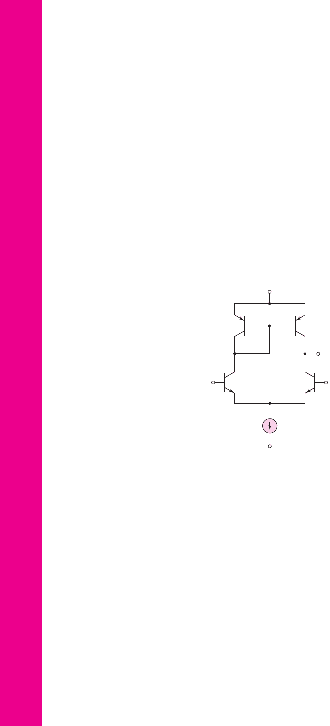
*D11.71 Design a BJT diff-amp with an active load similar to the configuration in
Figure P11.70 except that the input devices are to be pnp transistors and
V
+
V
–
V
–
V
–
V
–
Q
3
Q
1
Q
4
Q
5
Q
6
Q
7
v
1
v
2
Q
2
I
Q
I
Q1
Figure P11.67
V
+
= 10 V
V
–
= –10 V
v
1
M
3
M
4
M
1
M
2
I
Q
= 0.2 mA
R
1
= 1 kΩR
1
= 1 kΩ
v
O
v
2
Figure P11.68
nea80644_ch11_753-850.qxd 6/19/09 4:38 AM Page 842 pmath DATA-DISK:Desktop Folder:18.6.09:MHDQ134-11:

Chapter 11 Differential and Multistage Amplifiers 843
the active load will have npn transistors. Using the same parameters as in
Problem 11.70, determine the small-signal differential-mode voltage gain.
D11.72 Reconsider the diff-amp specifications listed in Problem 11.45. Design an
all-CMOS diff-amp with the configuration in Figure 11.32 to meet the
specifications. The NMOS transistor parameters are
V
TN
= 0.4
V,
k
n
= 100 μ
A/V
2
, and
λ
n
= 0.025 V
−1
. The parameters of the PMOS tran-
sistors are
V
TP
=−0.4
V,
k
p
= 40 μ
A/V
2
, and
λ
p
= 0.04 V
−1
.
D11.73 An all-CMOS diff-amp, including the current source circuit, with the con-
figuration in Figure 11.32 is to be designed to have a differential-mode
gain of
A
d
= 240
. The bias voltages are
V
+
= 3
V and
V
−
=−3
V. The
total power dissipation in the circuit is to be limited to 0.8 mW. Assume
the NMOS transistor parameters are
V
TN
= 0.4
V,
k
n
= 100 μ
A/V
2
, and
λ
n
= 0.02 V
−1
. Assume PMOS transistor parameters of
V
TP
=−0.4
V,
k
p
= 40 μ
A/V
2
, and
λ
p
= 0.03 V
−1
.
D11.74 The differential amplifier with the configuration shown in Figure 11.36 is
to be designed to achieve a differential-mode voltage gain of
A
d
= 400
.
The circuit parameters are to be
V
+
=+5
V,
V
−
=−5V
, and
I
Q
= 200 μA
. The available transistors have parameters for the PMOS of
V
TP
=−0.5V
,
k
p
= 40 μA/V
2
, and
λ
p
= 0.02 V
−1
, and for the NMOS
of
V
TN
=+0.5
V,
k
n
= 80 μA/V
2
, and
λ
n
= 0.015 V
−1
.
*11.75 Consider the fully cascoded diff-amp in Figure 11.37. Assume
I
Q
= 80 μA
and transistor parameters of:
V
TN
= 0.8
V,
k
n
= 60 μA/V
2
,
λ
n
= 0.015 V
−1
,
V
TP
=−0.8V
,
k
p
= 25 μA/V
2
, and
λ
p
= 0.02 V
−1
.
The transistor width-to-length ratios are
W/L = 60/4
for transistors
M
1
–M
4
,
W/L = 40/4
for transistors M
5
–M
6
, and
W/L = 4/4
for transis-
tors M
7
–M
8
. (a) Determine the output resistance of the diff-amp. (b) Cal-
culate the differential-mode voltage gain of the diff-amp. (c) Find the
common-mode voltage gain of the diff-amp using a computer simulation.
11.76 Consider the diff-amp that was shown in Figure P11.63. The circuit
and transistor parameters are
V
+
= 2.8
V,
V
−
=−2.8
V,
I
Q
= 120 μ
A,
K
n
= K
p
= 0.2
mA/V
2
,
V
TN
=+0.3
V,
V
TP
=−0.3
V, and
λ
n
= λ
p
=
0.025 V
−1
. (a) Determine the differential-mode voltage gain. (b) What is
v
1
v
2
v
o
V
+
V
–
I
Q
Q
5
Q
6
Q
1
Q
3
Q
4
Q
2
Figure P11.70
nea80644_ch11_753-850.qxd 6/19/09 4:38 AM Page 843 pmath DATA-DISK:Desktop Folder:18.6.09:MHDQ134-11:
844 Part 2 Analog Electronics
the output resistance of the diff-amp? (c) What is the maximum common-
mode voltage that may be applied?
11.77 The diff-amp in Figure P11.63 is biased at
I
Q
= 0.5
mA. The transistor
parameters are
K
n
= K
p
= 0.25
mA/V
2
,
V
TN
= 0.4
V,
V
TP
=−0.4
V,
and
λ
n
= λ
p
= 0.02 V
−1
. (a) What are the minimum power supply volt-
ages if the common-mode input voltage is to be in the range
±3
V? As-
sume symmetrical supply voltages. (b) Determine the differential-mode
voltage gain.
11.78 The circuit and transistor parameters of the bipolar diff-amp shown in
Figure P11.78 are
I
Q
= 200 μA
,
β
npn
= 125
,
β
pnp
= 80
,
V
BE
(on) =
V
EB
(on) = 0.7V, V
AN
= 100
V, and
V
AP
= 60
V. (a) What are the mini-
mum power supply voltages (assume symmetrical supply voltages) if the
common-mode input voltage is to be in the range of
±2
V. (b) What is the
differential-mode voltage gain?
11.79 Repeat Problem 11.78 if
I
Q
= 120 μA
,
V
AN
= 75
V, and
V
AP
= 40
V. All
other parameters remain the same.
V
+
v
O
v
2
v
1
Q
3
Q
4
Q
1
Q
2
V
–
I
Q
Figure P11.78
Section 11.5 BiCMOS Circuits
11.80 (a) The Darlington pair circuit in Figure 11.45 has new bias current levels
of
I
BIAS1
= 0.25
mA and
I
BIAS2
= 0.50
mA. The transistor parameters are
K
n
= 0.2
mA/V
2
,
V
TN
= 0.4
V, and
λ = 0
for
M
1
; and
β = 150
,
V
BE
(on) = 0.7
V, and
V
A
=∞
for
Q
2
. Determine the small-signal para-
meters for each transistor and find the composite transconductance. (b) Re-
peat part (a) for bias currents of
I
BIAS1
= 0.05
mA and
I
BIAS2
= 0.50
mA.
11.81 Consider the BiCMOS diff-amp in Figure 11.44, biased at
I
Q
= 0.4
mA.
The transistor parameters for M
1
and M
2
are:
K
n
= 0.2
mA/V
2
,
V
TN
= 1
V, and
λ = 0.01 V
−1
. The parameters for Q
1
and Q
2
are:
β = 120
,
V
EB
(on) =
0.7 V, and
V
A
= 80
V. (a) Determine the differential-mode
voltage gain. (b) If the output resistance of the current source is
R
o
= 500 k
, determine the common-mode voltage gain using a com-
puter simulation analysis.
nea80644_ch11_753-850.qxd 6/19/09 4:38 AM Page 844 pmath DATA-DISK:Desktop Folder:18.6.09:MHDQ134-11:
Chapter 11 Differential and Multistage Amplifiers 845
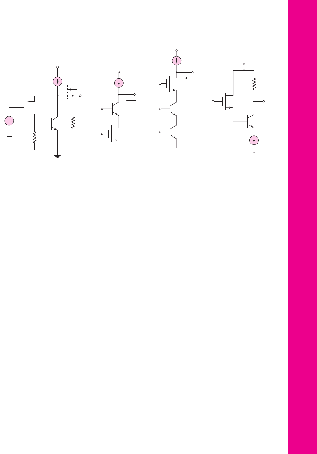
+5 V
I
Q
R
o
v
O
v
i
R
L
Q
2
M
1
R
1
=
8 kΩ
2.5 V
+
–
+
–
C
C
Figure P11.82
I
Q
I
Q
R
o
V
Bias
V
Bias2
V
Bias1
R
o
v
o
v
o
v
i
v
i
Q
1
M
1
V
+
V
+
(a) (b)
Figure P11.84
+10 V
R
C
=
20 kΩ
I
Q
= 0.2 mA
–10 V
M
1
Q
1
v
i
v
o
Figure P11.85
11.82 The BiCMOS circuit shown in Figure P11.82 is equivalent to a pnp bipolar
transistor with an infinite input impedance. The bias current is
I
Q
= 0.5
mA.
The MOS transistor parameters are
V
TP
=−0.5
V,
K
p
= 0.7
mA/V
2
, and
λ = 0
, and the BJT parameters are
β = 180
,
V
BE
(on) = 0.7
V, and
V
A
=∞
.
(a) Sketch the small-signal equivalent circuit. (b) Calculate the small-signal
parameters for each transistor. (c) Determine the small-signal voltage gain
A
v
= v
o
/v
i
for (i)
R
L
= 10
k
and (ii)
R
L
= 100
k
.
11.83 The bias current in the BiCMOS circuit shown in Figure P11.82 is
I
Q
= 0.8
mA. The transistor parameters are the same as described in Prob-
lem 11.82. (a) Sketch the small-signal equivalent circuit and calculate the
small-signal parameters for each transistor. (b) Determine the output resis-
tance as defined in the figure.
*11.84 The bias current I
Q
is 25
μA
in each circuit in Figure P11.84. The BJT
parameters are
β = 100
and
V
A
= 50
V, and the MOSFET parameters are
V
TN
= 0.8
V,
K
n
= 0.25
mA/V
2
, and
λ = 0.02 V
−1
. Assume the two
amplifying transistors M
1
and Q
1
are biased in the saturation region and
forward-active region, respectively. Determine the small-signal voltage
gain
A
v
= v
o
/v
i
and the output resistance R
o
for each circuit.
11.85 For the circuit shown in Figure P11.85, determine the small-signal voltage
gain,
A
v
= v
o
/v
i
. Assume transistor parameters of
V
TN
= 1
V,
K
n
=
0.2 mA/V
2
, and
λ = 0
for M
1
and
β = 80
and
V
A
=∞
for Q
1
.
Section 11.6 Gain Stage and Simple Output Stage
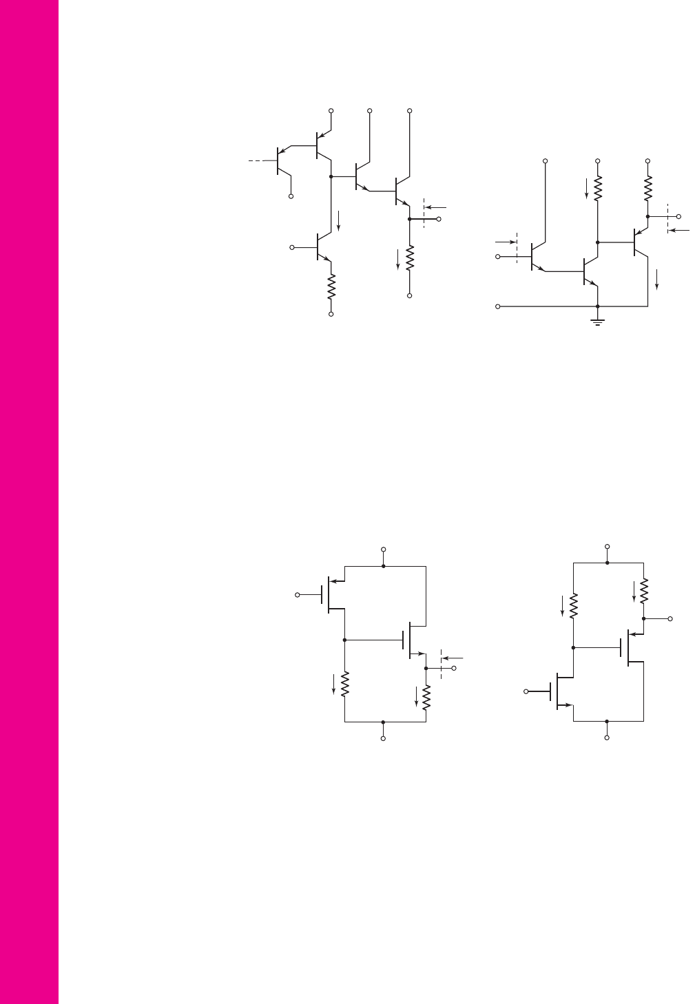
11.86 The output stage in the circuit shown in Figure P11.86 is a Darlington pair
emitter-follower configuration. Assume
β = 120
for all npn transistors
and
β = 90
for all pnp transistors. Let
V
A7
= 60
V for
Q
7
,
V
A11
= 120
V
for
Q
11
, and
V
A
=∞
for all other transistors. Determine the output resis-
tance
R
o
.
*11.87 For the circuit in Figure P11.87, the transistor parameters are
β = 100
and
V
A
=∞
. The bias currents in the transistors are indicated on the figure.
nea80644_ch11_753-850.qxd 6/19/09 4:38 AM Page 845 pmath DATA-DISK:Desktop Folder:18.6.09:MHDQ134-11:
846 Part 2 Analog Electronics
Determine the input resistance R
i
, the output resistance R
o
, and the small-
signal voltage gain
A
v
= v
o
/v
in
.
11.88 Consider the circuit in Figure P11.88. The bias currents I
1
and I
2
are such
that a zero dc output voltage is established. The transistor parameters are:
K
p
= 0.2
mA/V
2
,
K
n
= 0.5
mA/V
2
,
V
TP
=−0.8
V,
V
TN
=+0.8
V, and
λ
n
= λ
p
= 0.01 V
−1
. Determine the small-signal voltage gain
A
v
= v
o
/v
in
and the output resistance R
o
.
11.89 The bias currents in the circuit shown in Figure P11.89 are
I
1
= 0.25
mA
and
I
2
= 1.0
mA. The transistor parameters are
K
n
= 0.5
mA/V
2
,
K
p
= 1.0
mA/V
2
,
V
TN
= 0.8
V,
V
TP
=−0.8
V, and
λ
n
= λ
p
= 0.02
V
−1
.
(a) Determine the resistor values
R
1
and
R
2
such that the dc value of the
output voltage is zero. (b) Sketch the small-signal equivalent circuit and
find the small-signal transistor parameters. (c) Determine the small-signal
voltage gain
A
v
= v
o
/v
in
. (d) Determine the output resistance
R
o
.
R
i
V
+
V
+
V
+
v
in
v
O
R
o
I
Q
=
0.5 mA
I
C3
=
1 mA
Q
1
Q
2
Q
3
+
–
50 kΩ 5 kΩ
Figure P11.87
R
o
v
O
R
4
= 5 kΩ
Q
8
R
3
= 0.2 kΩ
Bias
I
Q
= 0.2 mA
I
C8
= 1 mA
Q
9
Q
11
Q
7
Q
6
V
–
V
–
V
–
V
+
V
+
V
+
Figure P11.86
V
+
= 5 V
V
–
= –5 V
v
in
v
O
M
1
M
2
R
o
I
1
I
2
R
1
= 35 kΩ
R
2
= 5 kΩ
Figure P11.88
V
+
= 5 V
V
–
= –5 V
v
in
M
1
M
2
R
2
R
1
v
O
I
1
I
2
Figure P11.89
nea80644_ch11_753-850.qxd 6/19/09 4:38 AM Page 846 pmath DATA-DISK:Desktop Folder:18.6.09:MHDQ134-11:
Chapter 11 Differential and Multistage Amplifiers 847
Section 11.7 Simplified Op-Amp Circuits
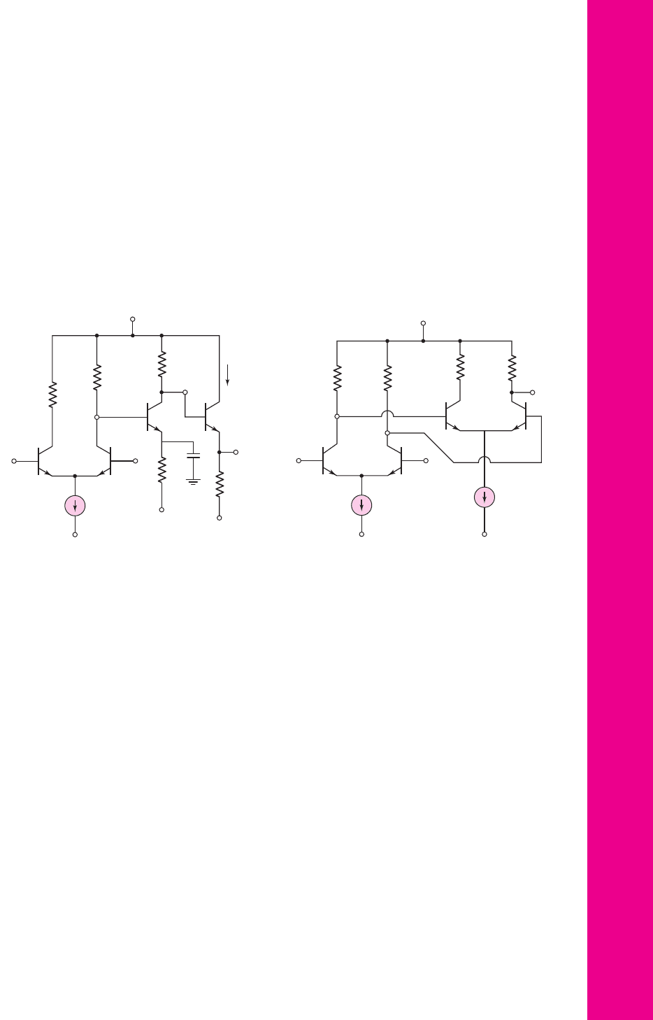
*11.90 Consider the multistage bipolar circuit in Figure P11.90, in which dc base
currents are negligible. Assume the transistor parameters are
β = 120
,
V
BE
(on) = 0.7
V, and
V
A
=∞
. The output resistance of the constant
current source is
R
o
= 200
k
. (a) For
v
1
= v
2
=−1.5
V, design the
circuit such that
v
O2
= v
O
= 0
,
I
CQ3
= 0.25
mA, and
I
CQ4
= 2
mA.
(b) Assuming
C
E
acts as a short circuit, determine the differential-mode
voltage gains
A
d1
= v
o2
/v
d
and
A
d
= v
o
/v
d
. (c) Determine the common-
mode gains
A
cm1
= v
o2
/v
d
and
A
cm
= v
o
/v
d
, and the overall
CMRR
dB
.
*D11.91 The circuit in Figure P11.91 has two bipolar differential amplifiers in
cascade, biased with ideal current sources I
Q1
and I
Q2
. Assume the
transistor parameters are
β = 180
and
V
A
=∞
. (a) Design the circuit
such that
v
o1
= v
o2
= 2
V and
v
O4
= 6
V when
v
1
= v
2
= 0
. (b) De-
termine the differential-mode voltage gains
A
d1
= (v
o1
−v
o2
)/v
d
and
A
d
= v
o4
/v
d
.
*11.92 The transistor parameters for the circuit in Figure P11.92 are:
β = 200
,
V
BE
(on) = 0.7
V, and
V
A
= 80
V. (a) Determine the differential-mode
voltage gain
A
d
= v
o3
/v
d
and the common-mode voltage gain
A
cm
=
v
o3
/v
cm
. (b) Determine the output voltage
v
o3
if
v
1
= 2.015
sin
ωt
V and
v
2
= 1.985
sin
ωt
V. Compare this output to the ideal output that would be
obtained if
A
cm
= 0
. (c) Find the differential-mode and common-mode
input resistances.
*11.93 For the transistors in the circuit in Figure P11.93, the parameters are:
K
n
=
0.2 mA/V
2
,
V
TN
= 2
V, and
λ = 0.02 V
−1
. (a) Determine the dif-
ferential-mode voltage gain
A
d
= v
o3
/v
d
and the common-mode voltage
gain
A
cm
= v
o3
/v
cm
. (b) Determine the output voltage v
o3
if
v
1
= 2.15
sin
ωt
V and
v
2
= 1.85
sin
ωt
V. Compare this output to the ideal output that
would be obtained if
A
cm
= 0
.
V
+
= 5 V
V
–
= –5 V
V
–
= –5 V
V
–
= –5 V
R
R
v
O2
I
CQ4
R
E1
R
E2
I
Q
= 0.5 mA
v
1
v
2
Q
1
Q
2
Q
3
Q
4
v
O3
R
C
v
O
C
E
Figure P11.90
R
C1
v
1
v
2
v
O1
v
O2
v
O4
Q
1
Q
2
Q
3
Q
4
R
C1
R
C2
V
+
= 10 V
I
Q1
= 0.2 mA
I
Q2
= 0.4 mA
V
–
= –10 VV
–
= –10 V
R
C2
Figure P11.91
nea80644_ch11_753-850.qxd 6/19/09 4:38 AM Page 847 pmath DATA-DISK:Desktop Folder:18.6.09:MHDQ134-11: