Watts J.F., Wolstenholme J. An Introduction to Surface Analysis by XPS and AES
Подождите немного. Документ загружается.

DEPTH PROFILING
BY
EROSION
WITH
NOBLE
GAS
IONS
97
If
we
make
the
approximation that
the
atoms
are in a
cubic array then
the
number
of
atoms
in 1 cm
2
is
(dN/w)
.
Thus,
if the
beam
is
rastered
over
an
area
of A
cm
2
,
the
number
of
surface atoms
in the
rastered area
is
A([dN]/w)
2
/
3
. Similarly,
the
layer thickness
is
[wf(dN)]
1
^. Now,
the
number
of
atomic layers removed
per
second
is the
number
of
atoms
removed
per
second divided
by the
number
of
atoms
at the
surface
under
the ion
beam:
jy
2
>i
Layers
per
second
—
•—/[A(pN/w]
''}
(4.5)
To get to the
etch
rate
we
have
to
multiply this expression
by the
layer
thickness:
(
w
\
Etch
rate
= —
\pNj
IY
e
This
simplifies
to:
Etch
rate
-
IYw/(AepN)
cms
–1
(4.7)
For
greater convenience,
if the
etch rate
is
expressed
in nm
s
–1
,
the
beam
current
in uA,
area
in mm and eN as 10
5
coulombs
(a
good
approxima-
tion)
then
the
expression becomes:
Etch
rate
=
10
–2
IYw/(pA)
nm s
–1
(4.8)
4.2.4 Factors
affecting
the
etch
rate
Material
The
sputter
rate
depends upon
the
chemical nature
of the
material,
not
only
the
elements present
but
also their chemical state.
It is
difficult
to
predict
the
sputter yield
for a
material
but
there
are a
number
of
com-
puter simulations available. Some
of
these
can
predict
sputter yields
of
elements
with reasonable accuracy
but
they become less reliable when
applied
to
compounds
or
alloys.
It is
usually preferable
to
measure
the
sputter yield experimentally under
the
conditions normally employed.
98
COMPOSITIONAL
DEPTH PROFILING
Ion
current
From Equation (4.8),
above,
it can be
seen
that
the
etch
rate
is
directly
proportional
to the ion
current.
It
should therefore
be
possible
to in-
crease
the
etch
rate
by
using
the
maximum beam current available.
However,
in a
normal
ion gun the
spot
size
of the
beam increases with
increasing beam current
and so the
rastered area must
be
increased
to
ensure
that
the
crater
bottom
remains
flat.
With this
in
mind,
simply
increasing
the
beam current will
not
necessarily increase
the
etch rate.
It
is
the ion
beam current density which
is the
important parameter rather
than merely
the
current.
Ion
energy
In
the
energy range normally employed
in XPS and
Auger
profiling
the
sputter
yield increases with
ion
energy.
At
high energy,
the
sputter
yield
will
reach
a
maximum. Higher energies also mean smaller
spot
sizes
at a
given beam current
and so
will lead
to
better
crater
quality.
The
higher etch
rate
will, however,
be
accompanied
by
poorer
depth resolution because
the
ions
can
penetrate
deeper
into
the
material causing atomic mixing.
Nature
of the ion
beam
In
XPS and
Auger profiling,
it is
customary
to use the
ions
of the
noble
gases
for
sputtering.
In the
energy range which
is
normally used, sputter
yield
increases with increasing atomic mass; xenon ions provide higher
etch rates than argon
and
helium ions provide very much lower sputter
yields
than argon.
In
addition,
the
larger ions penetrate
a
shorter dis-
tance into
the
material
and
therefore allow better depth resolutions
to be
obtained. This
all
points
to the use of
xenon
as the ion
beam but,
because
of its
significantly
higher
cost,
xenon
is
seldom used;
in
practice
argon
is the gas
which
is
selected.
Angle
of
incidence
As
the
angle
of
incidence (measured
from
the
sample normal)
is in-
creased,
the
sputter yield increases reaching
a
maximum
at
about
60°.
Above this angle
it
decreases rapidly.
The way in
which
the
sputter yield
DEPTH PROFILING
BY
EROSION
WITH
NOBLE
GAS
IONS
99
varies
with angle
is
difficult
to
predict because
it
depends upon
the
material
being sputtered
and the
nature
of the ion
beam.
However,
since
an
angle
of 60°
provides high sputter yields
and
good
depth resolution,
many
commercial instruments
are
designed with
the ion
incidence angle
close
to
this angle.
4.2.5 Factors
affecting
the
depth
resolution
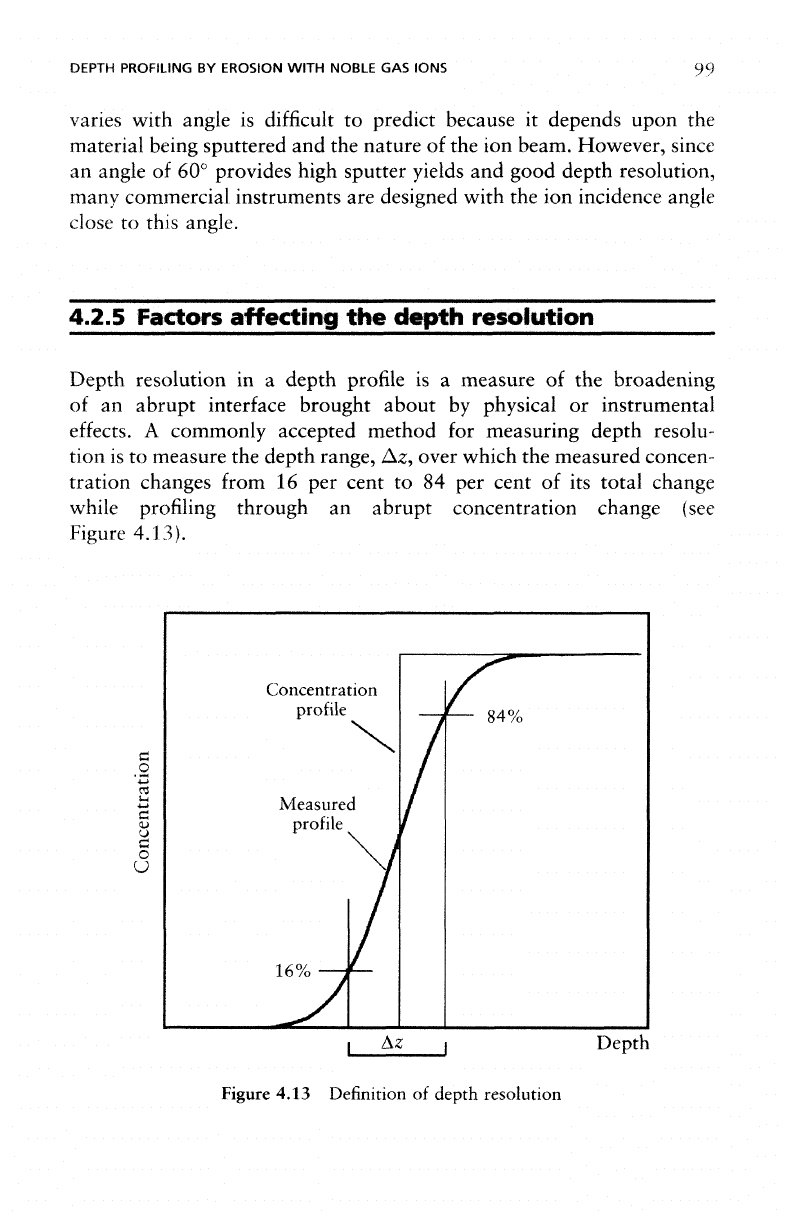
Depth
resolution
in a
depth
profile
is a
measure
of the
broadening
of
an
abrupt interface brought about
by
physical
or
instrumental
effects.
A
commonly accepted method
for
measuring depth resolu-
tion
is to
measure
the
depth range,
Az,
over which
the
measured concen-
tration changes
from
16 per
cent
to 84 per
cent
of its
total change
while
profiling
through
an
abrupt concentration change (see
Figure
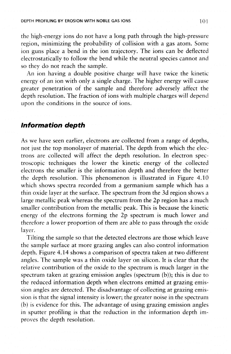
4.13).
§
d
o
U
Concentration
profile
Measured
profile
16%
84%
Depth
Figure
4.13
Definition
of
depth resolution
100
COMPOSITIONAL DEPTH PROFILING
Many
of the
factors which
affect
sputter rate also determine
the
depth
resolution
available. Some
of
these
factors relate
to the
characteristics
of
the
sample, some
to the
instrument
and
some
to the
physical process
of
sputtering.
Ion
beam characteristics
The
extent
to
which
the ion
beam characteristics
affect
depth resolution
generally
relates
to the
depth range
of the
ions
after
striking
the
sample.
This
is
because
the
passage
of an
energetic
ion
through
a
solid causes
atomic mixing along
the
whole trajectory
of the
ion.
Hence
low ion
energy, grazing incidence angles
and
heavy ions lead
to the
best depth
resolution because these minimize
the
depth range over which
mixing
can
occur.
Crater quality
The
crater must
be as
flat
as
possible over
the
analysis area.
If
this
is not
the
case then information
is
being collected
from
a
range
of
depths
and
resolution
suffers.
Generally,
the
raster
dimensions should
be at
least
five
ion
beam diameters
to get
good
flatness
over
a
reasonable distance
within
the
crater.
Beam
impurities
Chemical impurities
in the
beam
can be
minimized
by
using
a
high-purity
gas
feed. Other impurities
are
more
difficult
to
remove;
these consist
of
high-energy neutral species
and
ions with
a
multiple
charge.
High-energy neutrals
are
formed
by the
collision
of an
energetic
ion
with
a gas
atom during which there
is a
charge exchange process.
Fol-
lowing this process,
the
neutral species continue with their kinetic
en-
ergy
almost unaltered
but
without their positive charges. Neutral species
cannot
be
focused
or
scanned
and so
they
can
sputter
the
sample
in
an
undefined manner
and
disrupt
the
quality
of the
crater.
The
concen-
tration
of
neutral species
in the
beam
can be
minimized
by
providing
effective
pumping near
the
source region
of the ion
gun.
This means that
DEPTH
PROFILING
BY
EROSION
WITH
NOBLE
GAS
IONS
101
the
high-energy ions
do not
have
a
long path through
the
high-pressure
region,
minimizing
the
probability
of
collision with
a gas
atom. Some
ion
guns place
a
bend
in the ion
trajectory.
The
ions
can be
deflected
electrostatically
to
follow
the
bend while
the
neutral species cannot
and
so
they
do not
reach
the
sample.
An
ion
having
a
double positive charge
will
have twice
the
kinetic
energy
of an ion
with only
a
single charge.
The
higher energy will cause
greater penetration
of the
sample
and
therefore adversely
affect
the
depth resolution.
The
fraction
of
ions with multiple charges
will
depend
upon
the
conditions
in the
source
of
ions.
Information depth
As
we
have seen earlier, electrons
are
collected from
a
range
of
depths,
not
just
the top
monolayer
of
material.
The
depth
from which
the
elec-
trons
are
collected
will
affect
the
depth resolution.
In
electron spec-
troscopic techniques
the
lower
the
kinetic energy
of the
collected
electrons
the
smaller
is the
information depth
and
therefore
the
better
the
depth resolution. This phenomenon
is
illustrated
in
Figure 4.10
which shows spectra recorded from
a
germanium sample which
has a
thin oxide layer
at the
surface.
The
spectrum from
the 3d
region shows
a
large metallic peak whereas
the
spectrum from
the 2p
region
has a
much
smaller
contribution
from
the
metallic peak. This
is
because
the
kinetic
energy
of the
electrons forming
the 2p
spectrum
is
much
lower
and
therefore
a
lower proportion
of
them
are
able
to
pass through
the
oxide
layer.
Tilting
the
sample
so
that
the
detected electrons
are
those which leave
the
sample surface
at
more grazing
angles
can
also
control
information
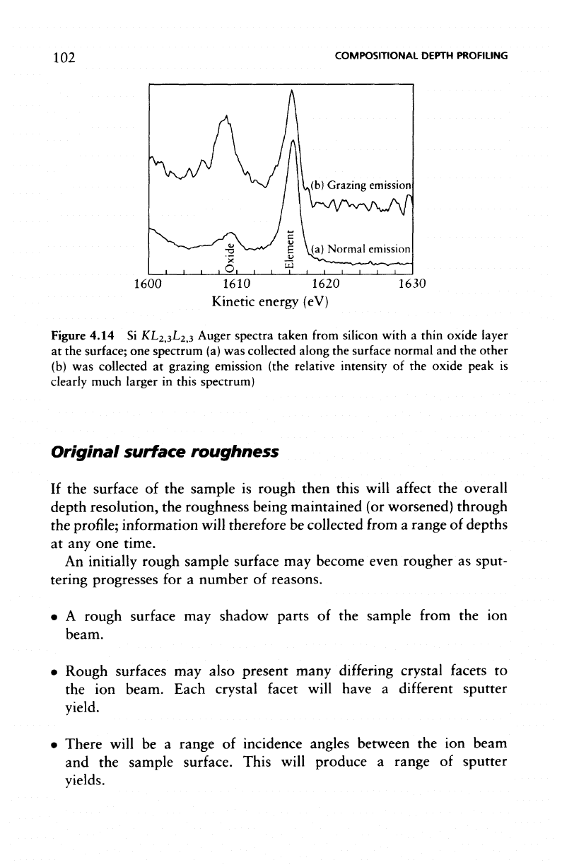
depth. Figure 4.14 shows
a
comparison
of
spectra taken
at two
different
angles.
The
sample
was a
thin oxide layer
on
silicon.
It is
clear that
the
relative
contribution
of the
oxide
to the
spectrum
is
much larger
in the
spectrum
taken
at
grazing emission angles (spectrum (b)); this
is due to
the
reduced information depth when electrons emitted
at
grazing emis-
sion
angles
are
detected.
The
disadvantage
of
collecting
at
grazing emis-
sion
is
that
the
signal intensity
is
lower;
the
greater noise
in the
spectrum
(b)
is
evidence
for
this.
The
advantage
of
using grazing emission angles
in
sputter profiling
is
that
the
reduction
in the
information depth
im-
proves
the
depth resolution.
102
COMPOSITIONAL
DEPTH PROFILING
1600 1610 1620
Kinetic
energy
(eV)
1630
Figure
4.14
Si
KL
2,3
L
2,3
Auger spectra taken
from
silicon
with
a
thin oxide
layer
at the
surface;
one
spectrum
(a) was
collected along
the
surface
normal
and the
other
(b)
was
collected
at
grazing emission (the
relative
intensity
of the
oxide peak
is
clearly
much larger
in
this spectrum)
Original
surface
roughness
If
the
surface
of the
sample
is
rough then this
will
affect
the
overall
depth resolution,
the
roughness being maintained
(or
worsened) through
the
profile; information will therefore
be
collected
from
a
range
of
depths
at any one
time.
An
initially
rough sample
surface
may
become even rougher
as
sput-
tering progresses
for a
number
of
reasons.
• A
rough
surface
may
shadow parts
of the
sample
from
the ion
beam.
•
Rough surfaces
may
also
present
many
differing
crystal facets
to
the ion
beam. Each crystal
facet
will
have
a
different
sputter
yield.
•
There
will
be a
range
of
incidence angles
between
the ion
beam
and the
sample surface. This
will
produce
a
range
of
sputter
yields.
DEPTH PROFILING
BY
EROSION
WITH
NOBLE
GAS
IONS
103
Induced roughness
The
sputtering process
can
cause
the
surface
to
become rough during
the
profiling
experiment, degrading
the
resolution
as a
function
of
depth.
This problem
can be
significantly reduced
or
eliminated
by
rotating
the
sample
beneath
the ion
beam (azimuthal rotation) during
the
sputtering
cycles.
Many commercial instruments
now
offer
sample stages which
incorporate azimuthal rotation.
Preferential
sputtering
In
a
multi-component sample
the
sputter yields from
different
elements
can be
different.
Under these conditions there will
be
roughening which
may
not be
controllable
by
azimuthal rotation. Furthermore,
the
surface
concentration
of the
elements will
be
different
from
the
bulk concentra-
tion
and so
quantification
of the
data will
be
difficult,
requiring
the
application
of
correction factors.
Redeposition
of
sputtered material
Care
must
be
taken
to
avoid
the
redeposition
of
sputtered species
onto
samples awaiting analysis. Furthermore,
if the
etch crater
is
small,
ma-
terial
can be
sputtered
from
the
crater walls
and
redeposited within
the
analysis
area.
4.2.6
Calibration
Depth
profile
data
are
presented
as
elemental intensity versus etch time,
and a
major
problem
in
sputter depth profiling
is
converting this etch
time
scale
to a
depth scale. Although,
in
special cases,
it is
possible
to
calibrate
ion
guns
for a
particular material,
it is a
time-consuming
pro-
cedure
and,
more often,
the
sputter rate
is
related
to an
international
standard.
The
current standard
is a
Ta
2
O
5
/Ta
foil
with
an
accurately
determined
oxide
thickness
(30 nm or 100
nm).
Thus,
it is
possible
to
report
a
sputter
rate
and
also
an
interface width
for the ion gun and the
conditions
used
in any
particular piece
of
work.
104
COMPOSITIONAL
DEPTH
PROFILING
4.2.7
Ion gun
design
In
addition
to
providing
a
means
of
compositional depth
profiling
in
surface
analysis,
ion
guns
may be fitted to a
spectrometer
for
additional
purposes such
as
large area specimen cleaning
or as the
primary beam
in
ion
beam analysis methods such
as ISS or
SIMS.
The
requirements
for
each application
are
slightly
different
and
there
are
several
different
designs
in
common use.
The
three most widely employed types
of ion
source
for
surface
anal-
ysis
are,
in
order
of
increasing performance
and
cost,
the
cold cathode
static
spot
gun,
the
electron impact
ion
source,
and the
duoplasmatron
type
of ion
gun. Liquid metal
ion
guns also
find use in
surface analysis,
principally
for
small area depth
profiling
and
imaging SIMS; their
use is
rare
on XPS and AES
instruments.
Cold cathode
ion
guns
In
the
cold cathode type
of gun a
variable potential
of
1-l0
kV is
utilized
in
conjunction with
an
external magnet
to
produce
a
discharge
in
the
ionization region
of the gun
into which argon
or
another inert
gas
flows to a
pressure
of
about 10
-6
mbar.
The
positively charged ions
are
extracted
and the
beam shaped
by a
simple
electrostatic
lens.
These
guns
generally
give
a
static spot size
of
5–10
mm
depending
on the
applied
focus
potential. They
are
recommended
for
specimen cleaning,
but
with
the
addition
of an
aperture assembly below
the
focus
electrode, they
can
give
remarkably uniform etch craters.
The
main disadvantage
is the
production
of
neutral species which
are not
deflected
by the
focus
po-
tential
and
give rise
to a
'sub-crater'
of
about 5-10
per
cent
of the
area
of
the
main crater.
The
maximum current
available
with this type
of gun
is
of the
order
of 50 uA.
Electron impact
ion
guns
Ion
guns based
on the
electron impact source
are
very
popular
for
depth
profiling
applications
in XPS and
AES. This
is due to a
combination
of
their
compact
design
and
lower
cost
compared with duoplasmatron
de-
signs.
In
addition,
the ion
current output
of
this type
of ion gun at
very
low
DEPTH PROFILING
BY
EROSION
WITH
NOBLE
GAS
IONS
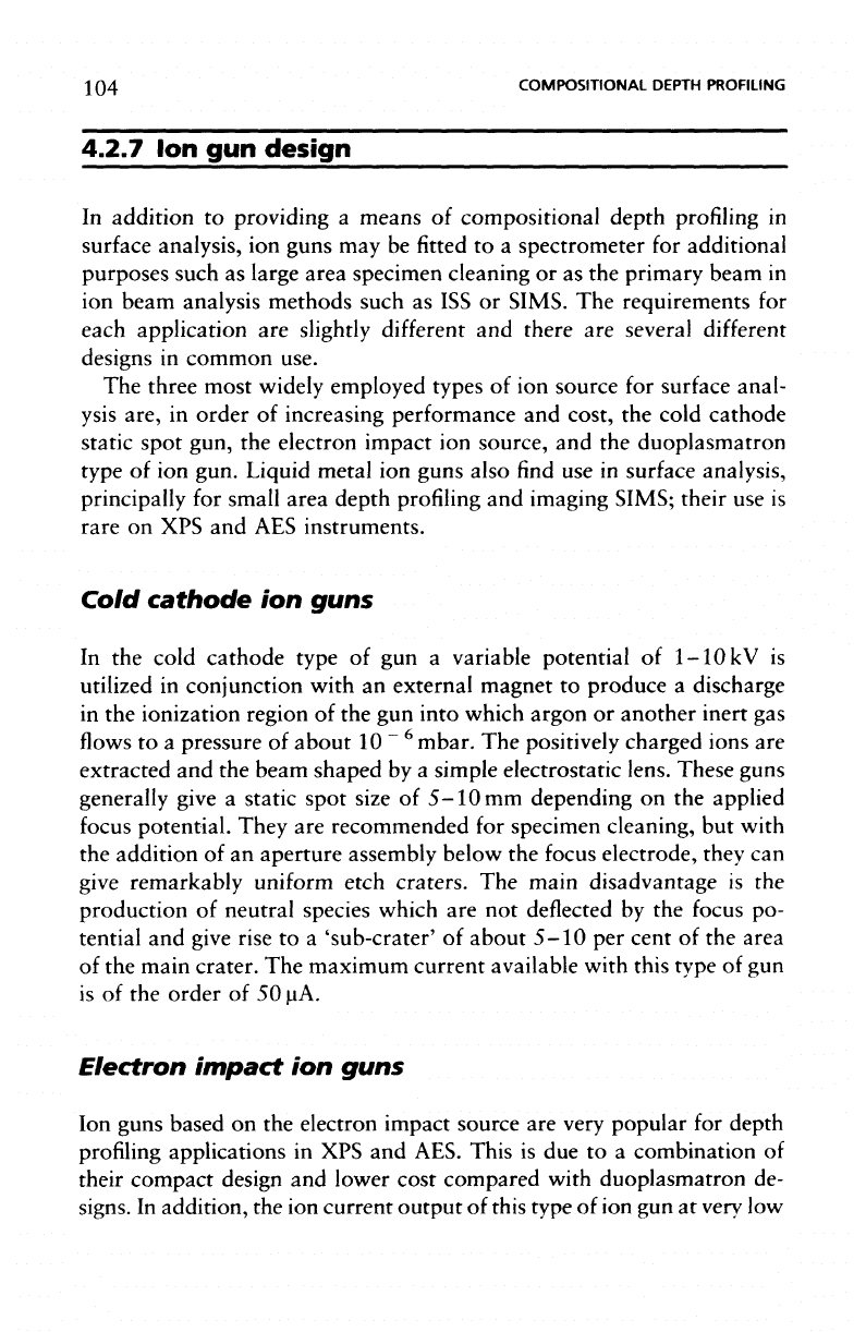
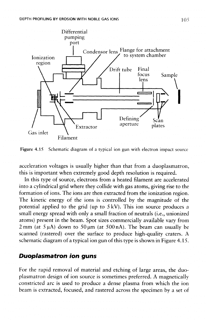
lonization
region
Differential
pumping
port
Condensor
lens
Flange
for
attachment
to
system
chamber
tube
Final
focus
Sample
lens
Defining
Scan
^
aperture
nlat-pc
Extractor
r
plates
Filament
Figure
4.15 Schematic diagram
of a
typical
ion gun
with
electron impact source
Gas
inlet
acceleration voltages
is
usually higher than that from
a
duoplasmatron,
this
is
important
when extremely
good
depth resolution
is
required.
In
this type
of
source,
electrons from
a
heated
filament are
accelerated
into
a
cylindrical grid where they collide with
gas
atoms,
giving rise
to the
formation
of
ions.
The
ions
are
then extracted from
the
ionization region.
The
kinetic energy
of the
ions
is
controlled
by the
magnitude
of the
potential applied
to the
grid
(up to 5
kV). This
ion
source produces
a
small
energy spread with only
a
small fraction
of
neutrals (i.e., unionized
atoms)
present
in the
beam. Spot sizes commercially available vary
from
2mm (at
5uA) down
to 50 um (at 500
nA).
The
beam
can
usually
be
scanned (rastered) over
the
surface
to
produce high-quality
craters.
A
schematic diagram
of a
typical
ion gun of
this type
is
shown
in
Figure 4.15.
Duoplasmatron
ion
guns
For
the
rapid removal
of
material
and
etching
of
large areas,
the
duo-
plasmatron design
of ion
source
is
sometimes preferred.
A
magnetically
constricted
arc is
used
to
produce
a
dense plasma from which
the ion
beam
is
extracted, focused,
and
rastered across
the
specimen
by a set of
106
COMPOSITIONAL
DEPTH
PROFILING
deflector
plates.
Ion
guns based
on a
duoplasmatron source provide
an
intense
source
with
a
narrow
energy
spread,
making them suitable
for
small
spot
focusing.
The
current density achieved with such
an ion gun
can
be
high, leading
to
high etch rates. Duoplasmatron
ion
sources
are
available
in a
range
of
spot sizes varying
from
2 mm
(providing
80 uA of
ion
current
and
with
a field of
view
of
approximately
15 mm x 15 mm)
to
better than
5 urn
(providing
a
maximum current
of 5 uA and a
2mm x 2mm field of
view).
The
former
is
ideal
for
large area depth
profiling
in
non-monochromated
XPS
while
the
latter
finds
extensive
use
as a
primary source
in the ion
beam analysis
of
materials.
With both duoplasmatron
and
electron impact sources
the
beams
may
be
'purified' (i.e., removal
of
impurities
and
ions with
a
multiple charge)
by
the
addition
of a
Wien
filter (a
crossed magnetic
and
electrostatic
field
mass separator)
and a
small
deflection
within
the gun
design
to
eliminate neutrals. Such high-purity beams
are
not, however,
a
prereq-
uisite
for
good
quality
XPS and AES
sputter depth
profiling.
In
general,
the
only precaution necessary
is the
provision
of a
high-purity
gas
feed.
Liquid
metal
ion
guns
For
some applications, particularly when very small diameter
ion
beams
are
required, liquid metal
ion
guns
can be
used.
The
metal ions produced
by
this type
of gun are
usually
Ga
+
but
other materials have been used.
These
guns
can
produce
spot
sizes below
50 nm at
energies above
25
keV.
Although
the
beam current
at
these small
spot
sizes
is
very small (typically
~50
pA),
the
current densities
are
very high
and
large etch rates
can be
achieved over
a
small area. They have
the
added
advantage
that
they
do
not
impose
a gas
load
on the
vacuum system during operation. This type
of
ion gun is
commonly encountered
in
SIMS analysis, occasionally used
for
AES
profiling
and
rarely,
if
ever, used
in XPS
profiling.
A
major
application
of
this type
of gun is in
micromachining, often referred
to
as
focused
ion
beam (FIB) technology. Examples
of its use
are:
• for
producing
a
crater
in, for
example,
a
processed
silicon wafer prior
to the
analysis
of the
side wall using AES,
• for
repairing lithographic masks used
in the
production
of
semi-
conductor devices.