Yao N. Focused Ion Beam Systems: Basics and Applications
Подождите немного. Документ загружается.

4 µm
4 µm
Vector scan
Raster
Etching Deposition
(a)
(b)
400
380
360
340
320
300
280
260
240
220
200
180
160
140
120
100
80
60
40
20
0
–20
–40
–60
–80
–100
–100 –50 0 50 100 150 200 250 300 350 400
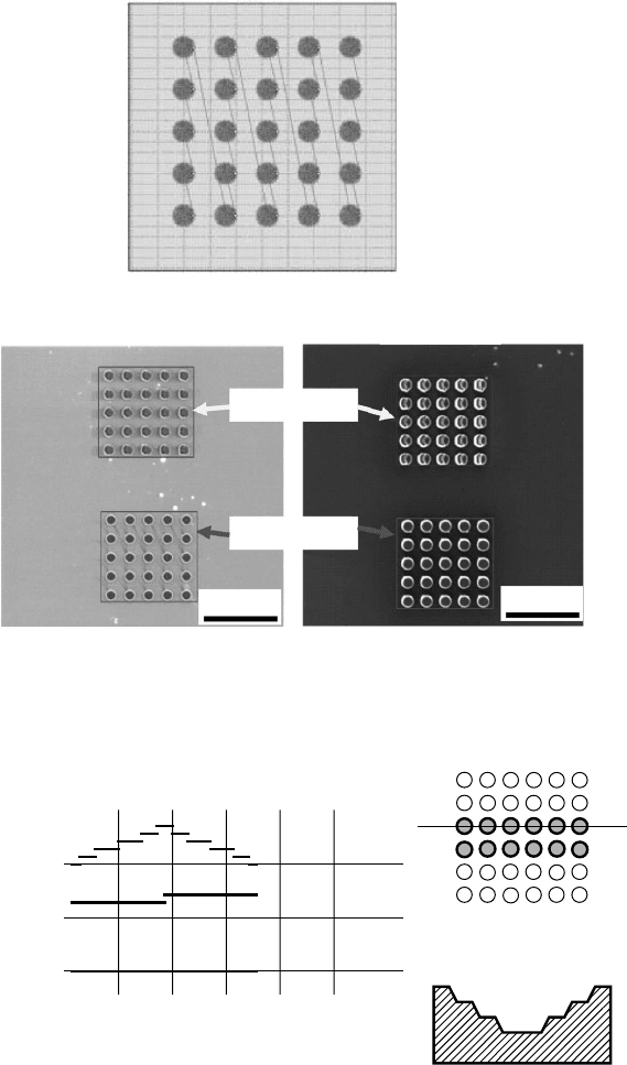
Figure 14.16 (a) Array of 5 · 5 circles, (b) results of etching and depo sition.
x
-scan signal
y
-scan signal
Blanking signal
Waveforms
A
A'
A
A'
Top view
Cross section
Figure 14.17 3D shaping.
Focused ion beam systems368
14.3 Role of FIB in nanotechnology
14.3.1 Nanotechnology
Figure 14.18 shows that to establish nanotechnology as an industrial product,
technology to create structures at the order of nanometers must be effectively
fused with mass production technology. For example, information available
on Intel’s home page shows the realization of manufacturing microscopic
devices by applying nanotechnology to integrated circuit manufacturing
technology, and by technological trends predicted by Moore’s law [7]. In
considering the role of the FIB tool in the development of nanotechnology,
the FIB tool can create structures of the order of micrometers to nanometers,
and since creating a photo mask is not required, the work takes compara-
tively less time resulting in an extremely useful tool.
14.3.2 Etching process
The biggest features of processing by FIB use the same ion beam in obser-
vation and processing. As shown in Figure 14.5, the observation region is
sputter etched as observation continues. This function lets you accurately and
precisely process extremely microscopic regions.
Microscopic etching process
In recent years, research into the shapes of electrodes with extremely small gaps
has greatly advanced. Objectives are many, including trying to make new
elements and trying to observe the types of phenomenon that occur in gaps at an
order of nanometers.
One experimental result [8] gives an example of a 5 nm width gap formed
by applying FIBs. Here the objective is to measure the electric properties of
high polymer materials at molecular levels using a manufactured electrode.
Mass production
Photo lithography
Prototype
Developing
New material
Miniaturization
Integration
Commercialization
Nanotechnology
Fusion
Figure 14.18 Nanotechnology as an indust rial product.
Focused ion beam systems as a multifunctional tool for nanotechnology 369
At the time the gap is made, the first step is to form a 12 nm wide gap in Ti by
sputter etching with the FIB, and the second step is milling of Ti on the mask
with Ar and etching the Au.
An SMI9200 (JFIB2300) FIB tool of SII with 7 nm secondary electron
resolution was used in this process. The latest tool was improved to have a
secondary electron resolution of 4 nm. In the case of the ion beam, the sec-
ondary electron resolution is almost the same as the beam diameter. This
performance has allowed even narrower gaps to be formed, compared with the
SMI9200.
Ordinarily, when expressing process performance with the FIB, there is a lot
of dispute over the maximum current and maximum current density because
of the desire to increase process throughput. However, if using the FIB tool as
an experimental tool for nanotechnology, using a beam current with a beam
diameter of less than 10 nm is essential. Processing microscopic areas precisely
and rapidly is required by setting a beam current that is optimized for making
structures.
Etching using graphic information
Processing must be performed as you monitor process conditions without
regard to size.
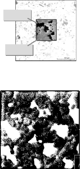
Figure 14.19 shows an example of a mask repair. The mask is made from a
light-penetrating glass board and a shading film such as light-shading chrome
film. Figure 14.19 shows an example of white defects where chrome originally
should have been, but are now missing. In this case, carbon is deposited at
the white defect area using the FIB deposition function [9].
In the case of a mask repair, you must avoid causing damage to the light
penetrating part by irradiating it with the ion beam more than is necessary.
The mask stage locates a
defect position using
the inspection system
coordinate and grabs
the defect ima
g
e.
The operation
software automatically
enhances
the edge signal.
The software defines the
repairing position from
the processed image, and adds
the repair area
to the SED ima
g
e.
Figure 14.19 An example of a mask repair.
Focused ion beam systems370
The ion beam must not irradiate the unnecessary part to prevent damage
being caused to the light penetrating glass. Consequently, graphic informa-
tion is used. In this example, a secondary ion detector is used in the detector.
Secondary ions are analyzed and the image is made binary from the presence
of chrome. Ion beams irradiate and carbon film is formed at the spot where
chrome should originally exist within the binary image; in other words,
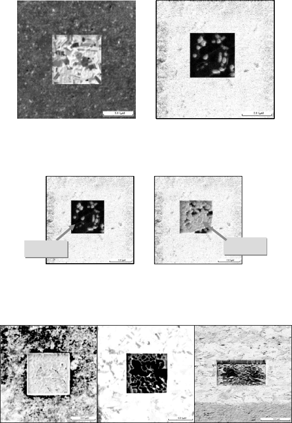
only at the white defect area. Figure 14.20 shows the results of two types of
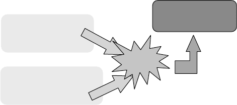
mask repair observed by an atomic force microscope (AFM). Both were
repaired using the FIB deposition function. A Cr binary mask is a type of
conventional mask, whereas a MoSi mask is a type of phase shift mask.
The technology developed for mask repair is explained in the following. This
technology makes use of graphical information to ensure precise processing.
As shown in Figure 14.9, it is difficult to obtain a flat bottom after Cu
milling. To improve the flatness of the bottom, graphic information was used.
The lower insulating film can be seen as etching of the Cu wire progresses.
Figure 14.21 shows the secondary electron image of Cu during the process.
The bright area is Cu and the dark area is SiO
2
.
Observation of the processed region during processing at a fixed period
seeks a binary image that is separated into bright regions and dark regions.
This binary image corresponds to whether there is Cu in the wire. Bitmap and
process data files are created from the binary image and ion beam irradiation
is performed by dot blanking scanning (Figure 14.22).
Observations are successively done during the process, bitmap and process
data files are updated, and the process advances.
Observation performed by secondary electrons has channeling contrast
that relies on grain shape. When creating a binary image based on the image,
100 [nm]0
2
1
3
2
1
0
[µm]
(a) (b)
100 [nm]0
2
1
2
1
0
[µm]
Figure 14.20 AFM image of a mask repair. (a) Binary deposition on Cr,
(b) deposition on MoSi.
Focused ion beam systems as a multifunctional tool for nanotechnology 371
areas having Cu can no longer be correctly recognized; therefore, secondary
ions are used. Images by secondary ions are contrast images that rely on the
quality of the material. Having been affected by channeling contrast, Cu
regions and regions without Cu cannot be discriminated (Figure 14.23).
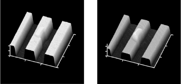
Figure 14.24 shows an example of a processed Cu wire using a secondary
ion image. It can be verified that only the Cu is being etched as the process
progresses.
Figure 14.25 introduces an example of a process implemented based on
bitmap and process data. A process is terminated when the entire processed
region becomes bright showing the insulation. Decelerated etching by water
is not used in this process. Remarkable improvement is shown compared
with the example (without gas) introduced in Figure 14.9.
Finally, the finishing process is done by decelerated etching using water
from the condition shown in Figure 14.25. Figure 14.26 shows that the Cu
Figure 14.22 Example of bitmap processed data.
SiO
2
Cu
Figure 14.21 Secondary electron image while processing Cu. Only the center
area has been processed.
Focused ion beam systems372
was cleanly removed. Thus, precision processing can be performed by getting
feedback from image information.
14.3.3 3D deposition
The first commercialized application of an FIB was mask repair and circuit
edit using deposition. Both of them use deposition in two dimensions.
(a) (b)
Figure 14.23 (a) Secondary electron and (b) secondary ion images during Cu
milling.
SiO
2
Cu
(a) (b)
Figure 14.24 Change in secondary ion image during Cu processing.
(a) Before etching, (b) after etching. The processed region is the center
area, the dark area is Cu, and the bright area is SiO
2
.
(a) (b) (c)
Figure 14.25 Processing using image information, with secondary ion (a),
secondary electron (b), and secondary electron tilted (c).
Focused ion beam systems as a multifunctional tool for nanotechnology 373
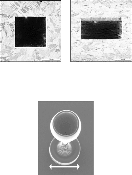
During the 1990s, research into three-dimensional deposition was reported.
The initial report was on a standing pillar, but the objective was to evaluate
the stability of the ion beam optic system by making three-dimensional
shapes. Afterwards, the performance and reliability of FIBs drastically
improved and three-dimensional shapes could be made stably.
Figure 14.27 shows an example of a micrometer sized wineglass made by 3D
deposition from carbon deposition developed by NEC, University of Hyogo,
and SII [10,11].
This 3D deposition must be performed more uniformly and with higher
gas density in the ion beam irradiation region than with 2D deposition.
Figure 14.28 shows this process diagrammatically.
A high density, uniform gas is supplied from the gas injector to the area of ion
beam irradiation. When forming a pillar, the ion beam continuously irradiated
the same position to produce the 3D structure. Overhanging shapes can be
achieved by widening the irradiation range in the horizontal direction. The wine
(a) (b)
Figure 14.26 Secondary electron image after the finishing process by
decelerated etching. (a) Top view; (b) bird’s-eye view.
2.75 µm
Figure 14.27 Example of 3D deposition. Material: carbon, process time ¼
600 s.
Focused ion beam systems374
glass was made by drawing a circle with a small radius by vector scanning and
then extending the radius.
Incidentally, when ion beams are irradiated to the surface of a specimen,
the surface is etched by ion beams. The deposition rate must be bigger than
the etching rate. Usually, the ion beam current for deposition is set low to
achieve a low etching rate.
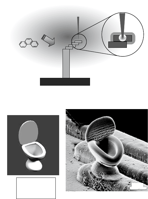
3D shaping using 3D-CAD data
Figure 14.29 shows an example using 3D-CAD data for 3D deposition. To
make this shape, 100 horizontal layers of slice data from a 3D-CAD were
created in .bmp format, and 100 carbon deposition film layers were created
Melting point: 99˚C
Boiling point: 340˚C
Diamond-like carbon (DLC) pillar
Si
Phenanthrene gas
Ga
+
Decomposition of
Adsorbed molecule
Secondary
electrons
Figure 14.28 The 3D deposition process.
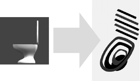
(3D-CAD)
30 kV, Ga
+
, 9 pA
Bitmap: 100 sheets
Sample: Si wafer
2 µm
Figure 14.29 Nano -toilet produced using 3D-CAD data for 3D deposition.
Focused ion beam systems as a multifunctional tool for nanotechnology 375
in order by the dot blanking scan method, beginning from the lowest layer
(Figure 14.30).
We were able to verify from our experimental results that the ion beam mold
method could be implemented in the same way as the light mold method, by
ion beam induced deposition. In order to realize more precise shapes in the
future, the following research needs to be pursued [12]:
1. Technology that corrects shape change from etching that progresses at the same
time as deposition film proximity deposition.
2. Establish a deposition data producing algorithm for realizing structures pushed
out at location s that don’t have a base.
14.3.4 3D Etching
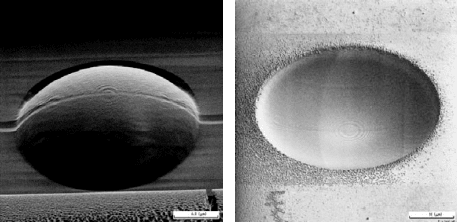
Figure 14.31 shows examples of lens shapes made by etching glass. In these
examples, 3D-CAD data were used. In a different way from that used for
deposition, space other than the manufactured object at the process space
is defined as etching space and creates .bmp files. In the examples in
Figure 14.31, sputter etching using dot blanking scanning progresses from
the top surface layer. This time, gas accelerated etching is used in order to
accurately realize specified shapes. When the redeposited material from
sputter etching remains in the process area, the gallium ion for the original
shape production is used to remove the redeposited material, and as a result
the intended shaped can no longer be realized. Thus, in the actual imple-
mentation, we try not to generate redeposited material using XeF
2
gas. The
results are that there is no effect from redeposition material and the intended
shape can be accurately reproduced.
Slicing to make
100 sheets of
the bitmap
data
Figure 14.30 3D data producing process.
Focused ion beam systems376
14.4 Unfolding of nanotechnology
This section outlines applications in micro-machining and nanotechnology of
microscopic 3D structure production technology that uses all the types of
process technology introduced in the previous chapters.
14.4.1 TEM sample preparation
The needs for observation, measurement, and analysis of ultra-microscopic
shapes are dramatically increasing together with the development of nano-
technology. In particular, there are increasing demands being made of obser-
vations by the transmission electron microscope (TEM). TEM is a tool that
irradiates accelerated electrons at high voltages of several 100 kV or greater on
samples with a thickness of 100 nm, and observes structures within the lamella
at atomic levels of resolution by detecting transmitted electrons. TEM is a
technology that already has a history going back several decades, but users
must make thin lamellae to observe by TEM. It takes more than one day for a
skilled technician to make a thin lamella using chemical polishing. With this
method, a specified spot on a miniaturized integrated circuit cannot be cut as a
specification.
However, Kirk et al.[13] developed a practical method of using FIB in
TEM specimen production. Automation has progressed, and, in the latest
report, TEM specimen production exceeding 100 specimens per day was
enabled by an FIB tool and system consisting of one microscope each with a
manipulator using the lift-out method (Figure 14.32)[14].
Beam position stability
The thickness of a lamella specimen is commonly 100 nm. Lamellae of
thicknesses of 40 nm or less are looked at depending upon the material and
(a) (b)
Figure 14.31 Lens shaped glass produced using 3D-CAD data. (a) Converging
lens, (b) concave lens.
Focused ion beam systems as a multifunctional tool for nanotechnology 377