Yao N. Focused Ion Beam Systems: Basics and Applications
Подождите немного. Документ загружается.

Preface
In the past few years, scientists have begun to gain the exquisite of controlling
the arrangement of matter on the nanometer scale (1 nm ¼10
9
m), a new
field called nanotechnology, consequently, has started to emerge. As the
foundation of nanotechnology, nanostructured materials take on an
enormously richer variety of properties and promise exciting new advances
in micromechanical, electronic, and magnetic devices as well as in molecular
fabrications. The structure–composition–processing–property relationships
for these sub-100 nm-sized materials can only be understood by employing
the new generation microscopes such as the focused ion beam system in
corporate with simultaneous operation of electron beam and in-situ analysis.
This book will highlight the principles and vast capabilities of this technique
and their applications in this fast-growing nanotechnology field and the
challenges in the twenty-first century.
xi
1
Introduction to the focused ion beam system
nan yao
Princeton University
1.1 Introduction
The frontier of today’s scientific and engineering research is undoubtedly in
the realm of nanotechnology: the imaging, manipulation, fabrication, and
application of systems at the nanometer scale. To maintain the momentum of
current research and industrial progress, the continued development of new
state of the art tools for nanotechnology is a clear necessity. In addition,
knowledge and innovative application of these tools is in increasingly high
demand as greater numbers of them come into use. The interdisciplinary field
of materials science, in particular, perpetually seeks imaging and analysis on
a smaller and smaller scale for a more complete understanding of materials
structure–composition–processing–property relationships. Moreover, the
ability to conduct material fabrication via precise micro- and nano-machin-
ing has become imperative to the progress of materials science and other
fields relying on nanotechnology.
An important tool that has successfully met these challenges and promises to
continue to meet future nanoscale demands is the focused ion beam (FIB)
system. The technology offers the unsurpassed opportunities of direct micro-
and nano-scale deposition or materials removal anywhere on a solid surface;
this has made feasible a broad range of potential materials science and nano-
technology applications. There has naturally been great interest in exploring
these applications, recently spurring the development of the two-beam FIB
system, often also called DualBeam or CrossBeam, a new and more powerful
tool that has advanced hand in hand with the complexity of new materials.
A focused ion beam system combines imaging capabilities similar to those
of a scanning electron microscope (SEM) with a precision machining tool.
Focused Ion Beam Systems: Basics and Applications, ed. N. Yao.
Published by Cambridge University Press. ª Cambridge University Press 2007.
1
It was developed as the result of research on liquid-metal ion sources (LMIS)
for use in space, conducted by Krohn in 1961 [1,2]. Liquid-metal ion sources
found novel applications in the areas of semiconductors and materials sci-
ence, and the FIB was commercialized in the 1980s as a tool mainly geared
toward the growing semiconductor industry [3]. In the development of
semiconductor fabrication, there is a constant struggle to improve the reso-
lution and speed of the lithographic technique. The use of photoresist and
masking improved the speed and reproducibility of the result, but not the
resolution, due to the fundamental and practical limitations imposed by the
wavelengths of the light used. Electron beam lithography was a marked
improvement in this area [4], due to the much smaller wavelength of a high
energy electron, often on the order of one to two hundredths of a nanometer
compared to the hundreds of nanometers associated with light. However,
electron beam (or e-beam) lithography is a comparatively slow process, and
often has difficulty penetrating harder materials without suffering from
considerable distortion effects due to local charge buildup. Electrons, though
easy to produce and accelerate, simply did not have the mass to penetrate
materials and remove atoms from a lattice quickly, and so e-beams have
stayed primarily in the realm of imaging, except in certain very specific
environments. Thus the demand for a lithographic method with the advan-
tage of short wavelengths, allowing higher resolution, but without the
drawbacks presented by the low mass of electrons, has found an answer in
the use of focused ion beams.
Fundamentally, a focused ion beam system produces and directs a stream
of high-energy ionized atoms of a relatively massive element, focusing them
onto the sample both for the purpose of etching or milling the surface and as a
method of imaging. The ions’ greater mass allows them to easily expel surface
atoms from their positions and produces secondary electrons from the sur-
face, allowing the ion beam to image the sample before, during, and after the
lithography process. The ion beam has a number of other uses as well,
including the deposition of material from a gaseous layer above the sample.
The ions in the beam strike atoms or molecules down onto the surface of the
sample, where intermolecular attractions fix them, and the implantation of
ions into a surface [5,6].
Today’s focused ion beam system utilizes a liquid-metal ion source at the
top of its column to produce ions, usually Ga
þ
. The ions are then pulled out
and focused into a beam by an electric field. They subsequently pass through
apertures and are scanned over the sample surface. The ion–atom collision is
either elastic or inelastic. Whereas elastic collisions result in the excavation of
surface atoms, a technique called sputtering or milling, inelastic collisions
Focused ion beam systems2
transfer some of the ions’ energy to either the surface atoms or electrons,
resulting in the emission of secondary electrons (those that become excited
enough to escape from their shell). Secondary ions are also emitted from the
surface following the secondary electrons.
The FIB system has four basic functions: milling, deposition, implantation,
and imaging; each will be discussed in detail in the following chapters. Milling
is a process that allows digging into the sample surface as a result of the use of
relatively heavy ions in the beam. It can also be easily converted into a
deposition system simply by adding a gas delivery device that allows the
application of certain materials, usually metals, to the surface of the material
where the beam strikes. When combined with milling, FIB deposition can
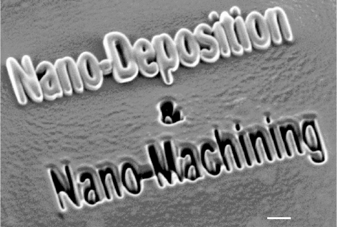
create almost any microstructure. Figure 1.1 represents a typical example of
such capability. Ion implantation is another important component of surface
modification that is available using the FIB. In addition to these three varia-
tions of material surface adaptation, the FIB system also has extensive imaging
capabilities. The large size of the ions provides advantages that are not
available with scanning electron microscopes or other imaging tools.
The FIB’s unique properties allow it to isolate specific sample regions so
that it only makes the necessary modifications without affecting the integrity
500 nm
Figure 1.1 A typical SEM image showing the simultaneous milling and
deposition capabilities of a two-beam FIB system. (Courtesy of Fibics
Incorporated.)
Introduction to the focu sed ion beam system 3
of the whole sample. With this technology the FIB can perform simple
techniques such as making probe holes as well as more complicated proce-
dures such as cutting a precise three-dimensional cross section of a sample.
The FIB, with its combination of drilling and deposition capabilities, is also
ideal for failure analysis and repair.
Using only an FIB system has some disadvantages, however, including that it
often causes some undesired damage to the sample. Obstacles associated with
the FIB, as well as the growing complexity of materials, has fueled the devel-
opment of a two-beam focused ion beam system: a system that combines both
electron beam and ion beam in a single microscope. Though the FIB system by
itself has a wide range of functions and applications, combining the FIB’s
precise imaging and machining abilities with the scanning electron microscope’s
high resolution, nondestructive imaging leads new and invaluable applications
to emerge that were previously impossible. The two-beam FIB excels at high
resolution structural, chemical, and geometric analyses of cross sections of
layers of material, a necessary feature for the examination of complex materials
and their synthetic analogs as well as for the analysis of phenomena that may
affect performance, durability, and reliability of many new materials. The
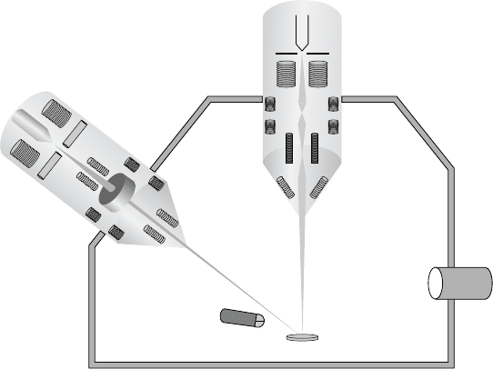
combination of SEM and FIB in a two-beam system, as shown schematically in
Figure 1.2, allows the electron and ion beams to work symbiotically to achieve
tasks beyond the limitations of either individual system.
Liquid gallium ion source
Suppressor
Extractor
Aperture
Alignment
octopole
Lens 1
Lens 2
Scan/stigmation
octopole
Ion beam
Secondary electron
detector
Sample
Anode
Alignment coils
Electron source
Lens 1
Lens 2
Scan/stigmation
coils
Lens 3 and pole piece
Electron beam
Vacuum fee
d
Figure 1.2 A schema tic diagram showing the configuration of a two-beam
focused ion beam system.
Focused ion beam systems4
In this chapter, we present a basic introduction of the two-beam FIB
system. Since ion beam and electron beam are the two key components of the
system, we start with a discussion of them first, followed by a discussion of
ion and electron sources used in the two-beam system. It is important to
explain the essential differences between electrons and ions in order to
understand how the properties of each affect the structure and functionality
of the FIB and the SEM. Following the discussion of properties of the ion
beam and electron beam and their emission sources, we will look at the ion
optics and electron optics responsible for focusing ions and electrons from
the source onto the sample in the column of a microscope. The detection of
secondary and backscattered charged particles from the sample to form
images will also be examined. Finally, we will introduce the two-beam system
and discuss its advantages versus a standalone SEM or FIB platform, and
how its enhanced capabilities open new channels for materials science and
nanotechnology.
1.2 Ion beam versus electron beam
All emissions can be sources of information, depending on the capabilities of
the instrument. The ejected signals from a focused ion beam or electron beam
can be collected, amplified, and then displayed to show detailed information
of the sample surface. When the ion beam is focused on one area for an
extended length of time, the continuous sputtering process gives the machine
another added use, that of removing surface material, which opens the door
for probing and milling applications. The FIB system can also be a deposi-
tion tool by injecting an organometallic gas in the path of the ion beam, just
above the sample surface. This technique allows for many kinds of material
fabrication at the micro- and nano-scales.
Since ions are significantly more massive than electrons (Table 1.1), the
FIB system has many more applications than a conventional imaging
instrument. The collision between the large primary ions of the beam and the
surface atoms causes surface alteration of various levels determined by the
dosage, overlap, dwell time, and many other ion beam variables. Such surface
alteration could not be achieved at the same level with electrons.
The ion beam and electron beam are based on the same principle and serve
many of the same purposes. They both consist of a stream of charged par-
ticles that is focused by a series of lenses and apertures onto a sample and
both employ similar methods to produce and accelerate the particles from
their source. Both systems can be used to image a sample, as well as to
perform etching and deposition.
Introduction to the focu sed ion beam system 5

The fundamental difference between the use of an ion beam and that of an
electron beam lies in their unique characteristics. The ion is much larger and
more massive than the electron and can be positively charged, whereas
electrons are always negatively charged. Since ions travel more slowly and
require greater fields to focus and control than electrons, different methods
are required to control massive ions versus electrons.
Size and mass can appreciably alter the interactions between the beam and
the sample (Table 1.1). When a beam of energetic particles, whether ions or
electrons, strikes a solid surface several interactions occur. Some particles are
backscattered from the surface layers; others are slowed down within the
solid. Unlike electrons, the relatively large ions have a hard time penetrating
the surface of a sample because it is much harder for them to pass through
individual atoms. Instead, their size increases their probability of interactions
with atoms, causing a rapid loss of energy. As a result, atomic ionization of
Table 1.1 Quantitative comparison of FIB ions and SEM electrons
Particle FIB SEM Ratio
Type Ga
þ
ion Electron
Elementary charge þ1 1
Particle size 0.2 nm 0.00001 nm 20 000
Mass 1.2 · 10
25
kg 9.1 · 10
31
kg 130 000
Velocity at 30 kV 2.8 · 10
5
m/s 1.0 · 10
8
m/s 0.0028
Velocity at 2 kV 7.3 · 10
4
m/s 2.6 · 10
7
m/s 0.0028
Velocity at 1 kV 5.2 · 10
4
m/s 1.8 · 10
7
m/s 0.0028
Momentum at 30 kV 3.4 · 10
20
kg m/s 9.1 · 10
23
kg m/s 370
Momentum at 2 kV 8.8 · 10
21
kg m/s 2.4 · 10
23
kg m/s 370
Momentum at 1 kV 6.2 · 10
21
kg m/s 1.6 · 10
23
kg m/s 370
Beam
Size nm range nm range
Energy up to 30 kV up to 30 kV ~
Current pA to nA range pA to mA range ~
Penetration depth
In polymer at 30 kV 60 nm 12000 nm 0.005
In polymer at 2 kV 12 nm 100 nm 0.12
In iron at 30 kV 20 nm 1800 nm 0.11
In iron at 2 kV 4 nm 25 nm 0.16
Average signal per 100 particles at 20 kV
Secondary electrons 100–200 50–75 1.33–4.0
Backscattered electron 0 30–50 0
Substrate atom 500 0 infinite
Secondary ion 30 0 infinite
X-ray 0 0.7 0
Focused ion beam systems6
the surface atoms and breaking of the chemical bonds between these atoms –
both processes involving mainly surface electrons – occur as the main ion–
atom interactions. Emission of secondary electrons usually accompanies
these processes as well as a change in the chemical state of the material.
Unlike in the case of an incident electron beam, however, the inner electrons
cannot be reached or excited by an ion beam and characteristic X-rays are
therefore unlikely to be generated.
The total length that the ion travels is known as its ‘‘penetration depth,’’ a
term which also applies to electrons, which often penetrate much deeper into
the sample than ions (Table 1.1). Because of the statistical nature of the
atomic collision, the penetration depth adheres to a symmetric Gaussian
distribution around the mean value. In the process of material modification,
the moving ion recoils one or more atoms in the sample, which results in the
recoiling of constituent atoms, leading to the creation of atomic defects along
the path of the ion beam.
The other difference between the two beam types, of course, is that the ion
beam has a much greater direct effect on its target, causing localized heating
and removing atoms beneath the focus, as well as implanting ions into the
surface and depositing atoms located above the sample onto it. Electron beams
generally cause little or no surface damage, have greater difficulty causing
deposition, and generally do not change the internal structure of the sample, as
the electrons left by the beam’s passage dissipate through conduction [7].
Ions are many times more massive than electrons and therefore carry
hundreds of times more momentum than electrons. In the ion–atom collision,
this momentum is transferred to the atoms on the surface of the material,
disturbing them from their aligned positions in a sputtering effect that has
important milling applications. The ion beam, as a direct result of the large
size and mass of the ion, surpasses the range of capabilities of the electron
beam by being able to remove atoms from the surface of a material in a
precise and controlled manner.
Gallium (Ga
þ
) ions are usually used in FIB systems for a number of
reasons. First, because of its low melting point, gallium only requires limited
heating and can conveniently be in liquid phase during operation; the lower
operating temperature also minimizes interdiffusion with the tungsten needle
substrate. Second, its mass is heavy enough to allow milling of the heavier
elements, but it is not so heavy that a sample is immediately destroyed. Third,
its low volatility at the melting point conserves the supply of metal and yields
a long source life of about 400 mA-hours/mg. Fourth, its low vapor pressure
allows Ga to be used in its pure form instead of in the form of an alloy
source, which would require an E · B mass separator in the optics column.
Introduction to the focu sed ion beam system 7