Masters G.M. Renewable and Efficient Electric Power Systems
Подождите немного. Документ загружается.

448 PHOTOVOLTAIC MATERIALS AND ELECTRICAL CHARACTERISTICS
less than 20% of the total. Critics of this decline point to the government’s lack
of enthusiasm to fund PV R&D. By comparison, Japan’s R&D budget is almost
an order of magnitude greater.
8.2 BASIC SEMICONDUCTOR PHYSICS
Photovoltaics use semiconductor materials to convert sunlight into electricity. The
technology for doing so is very closely related to the solid-state technologies used
to make transistors, diodes, and all of the other semiconductor devices that we
use so many of these days. The starting point for most of the world’s current
generation of photovoltaic devices, as well as almost all semiconductors, is pure
crystalline silicon. It is in the fourth column of the periodic table, which is
referred to as Group IV (Table 8.1). Germanium is another Group IV element,
and it too is used as a semiconductor in some electronics. Other elements that
play important roles in photovoltaics are boldfaced. As we will see, boron and
phosphorus, from Groups III and V, are added to silicon to make most PVs.
Gallium and arsenic are used in GaAs solar cells, while cadmium and tellurium
areusedinCdTecells.
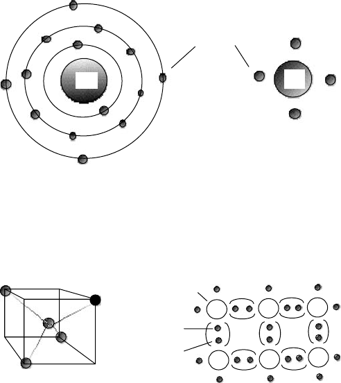
Silicon has 14 protons in its nucleus, and so it has 14 orbital electrons as well.
As shown in Fig. 8.4a, its outer orbit contains four valence electrons—that is, it
is tetravalent. Those valence electrons are the only ones that matter in electronics,
so it is common to draw silicon as if it has a +4 charge on its nucleus and four
tightly held valence electrons, as shown in Fig. 8.4b.
In pure crystalline silicon, each atom forms covalent bonds with four adja-
cent atoms in the three-dimensional tetrahedral pattern shown in Fig. 8.5a. For
convenience, that pattern is drawn as if it were all in a plane, as in Fig. 8.5b.
8.2.1 The Band Gap Energy
At absolute zero temperature, silicon is a perfect electrical insulator. There are no
electrons free to roam around as there are in metals. As the temperature increases,
TA BLE 8.1 The Portion of the Periodic Table of
Greatest Importance for Photovoltaics Includes the
Elements Silicon, Boron, Phosphorus, Gallium,
Arsenic, Cadmium, and Tellurium
I II III IV V VI
5B 6C 7N 8O
13 Al 14 Si 15 P 16 S
29 Cu 30 Zn 31 Ga 32 Ge 33 As 34 Se
47 Ag 48 Cd 49 ln 50 Sn 51 Sb 52 Te
BASIC SEMICONDUCTOR PHYSICS 449
+14 +4
(a) Actual (b) Simplified
Valence
electrons
Figure 8.4 Silicon has 14 protons and electrons as in (a). A convenient shorthand is
drawn in (b), in which only the four outer electrons are shown, spinning around a nucleus
with a +4charge.
Silicon
nucleus
Shared
valence
electrons
+4
+4
+4
+4
+4
+4
(a) Tetrahedral (b) Two-dimensional version
Figure 8.5 Crystalline silicon forms a three-dimensional tetrahedral structure (a); but it
is easier to draw it as a two-dimensional flat array (b).
some electrons will be given enough energy to free themselves from their nuclei,
making them available to flow as electric current. The warmer it gets, the more
electrons there are to carry current, so its conductivity increases with temperature
(in contrast to metals, where conductivity decreases). That change in conductivity,
it turns out, can be used to advantage to make very accurate temperature sensors
called thermistors. Silicon’s conductivity at normal temperatures is still very low,
and so it is referred to as a semiconductor. As we will see, by adding minute
quantities of other materials, the conductivity of pure (intrinsic) semiconductors
can be greatly increased.
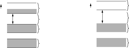
Quantum theory describes the differences between conductors (metals) and
semiconductors (e.g., silicon) using energy-band diagrams such as those shown
in Fig. 8.6. Electrons have energies that must fit within certain allowable energy
bands. The top energy band is called the conduction band, and it is electrons
within this region that contribute to current flow. As shown in Fig. 8.6, the
conduction band for metals is partially filled, but for semiconductors at absolute
zero temperature, the conduction band is empty. At room temperature, only about
one out of 10
10
electrons in silicon exists in the conduction band.
450 PHOTOVOLTAIC MATERIALS AND ELECTRICAL CHARACTERISTICS
Electron energy (eV)
E
g
Filled band
Filled band
Forbidden band
Conduction band
(partially filled)
Electron energy (eV)
E
g
Filled band
Filled band
Forbidden band
Conduction band
(empty at
T
= 0 K)
(a) Metals (b) Semiconductors
Gap
Gap
Figure 8.6 Energy bands for (a) metals and (b) semiconductors. Metals have partially
filled conduction bands, which allows them to carry electric current easily. Semiconductors
at absolute zero temperature have no electrons in the conduction band, which makes them
insulators.
The gaps between allowable energy bands are called forbidden bands, the most
important of which is the gap separating the conduction band from the highest
filled band below it. The energy that an electron must acquire to jump across the
forbidden band to the conduction band is called the band-gap energy, designated
E
g
. The units for band-gap energy are usually electron-volts (eV), where one
electron-volt is the energy that an electron acquires when its voltage is increased
by1V(1eV= 1.6 × 10
−19
J).
The band-gap E
g
for silicon is 1.12 eV, which means an electron needs to
acquire that much energy to free itself from the electrostatic force that ties it
to its own nucleus—that is, to jump into the conduction band. Where might
that energy come from? We already know that a small number of electrons get
that energy thermally. For photovoltaics, the energy source is photons of elec-
tromagnetic energy from the sun. When a photon with more than 1.12 eV of
energy is absorbed by a solar cell, a single electron may jump to the conduction
band. When it does so, it leaves behind a nucleus with a +4 charge that now
has only three electrons attached to it. That is, there is a net positive charge,
called a hole, associated with that nucleus as shown in Fig. 8.7a. Unless there
is some way to sweep the electrons away from the holes, they will eventually
recombine, obliterating both the hole and electron as in Fig. 8.7b. When recom-
bination occurs, the energy that had been associated with the electron in the
conduction band is released as a photon, which is the basis for light-emitting
diodes (LEDs).
It is important to note that not only is the negatively charged electron in the
conduction band free to roam around in the crystal, but the positively charged
hole left behind can also move as well. A valence electron in a filled energy band
can easily move to fill a hole in a nearby atom, without having to change energy
bands. Having done so, the hole, in essence, moves to the nucleus from which the
electron originated, as shown in Fig. 8.8. This is analogous to a student leaving
her seat to get a drink of water. A roaming student (electron) and a seat (hole)
are created. Another student already seated might decide he wants that newly
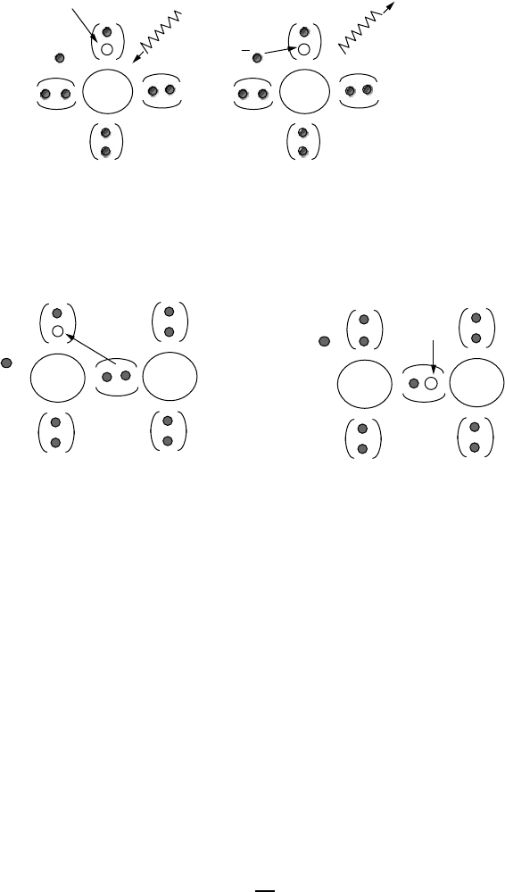
BASIC SEMICONDUCTOR PHYSICS 451
+4
Si
Free
electron
Hole
+
−
Photon
+4
Si
Photon
(a) Formation (b) Recombination
Figure 8.7 A photon with sufficient energy can create a hole–electron pair as in (a).
The electron can recombine with the hole, releasing a photon of energy (b).
+4
Si
+4
Si
+4
Si
+4
Si
Hole
+
(a) An electron moves to fill the hole (b) The hole has moved
Free
electron
Free
electron
Hole +
−
−
Figure 8.8 When a hole is filled by a nearby valence electron, the hole appears to move.
vacated seat, so he gets up and moves, leaving his seat behind. The empty seat
appears to move around just the way a hole moves around in a semiconductor.
The important point here is that electric current in a semiconductor can be carried
not only by negatively charged electrons moving around, but also by positively
charged holes that move around as well.
Thus, photons with enough energy create hole–electron pairs in a semicon-
ductor. Photons can be characterized by their wavelengths or their frequency as
well as by their energy; the three are related by the following:
c = λν (8.1)
where c is the speed of light (3 × 10
8
m/s), v is the frequency (hertz), λ is the
wavelength (m), and
E = hν =
hc
λ
(8.2)
where E is the energy of a photon (J) and h is Planck’s constant (6.626 × 10
−34
J-s).
452 PHOTOVOLTAIC MATERIALS AND ELECTRICAL CHARACTERISTICS
Example 8.1 Photons to Create Hole–Electron Pairs in Silicon What max-
imum wavelength can a photon have to create hole–electron pairs in silicon?
What minimum frequency is that? Silicon has a band gap of 1.12 eV and 1 eV =
1.6 × 10
−19
J.
Solution. From (8.2) the wavelength must be less than
λ ≤
hc
E
=
6.626 × 10
−34
J · s × 3 ×10
8
m/s
1.12 eV × 1.6 × 10
−19
J/eV
= 1.11 × 10
−6
m = 1.11 µm
and from (8.1) the frequency must be at least
ν ≥
c
λ
=
3 × 10
8
m/s
1.11 × 10
−6
m
= 2.7 × 10
14
Hz
For a silicon photovoltaic cell, photons with wavelength greater than 1.11 µm
have energy hν less than the 1.12-eV band-gap energy needed to excite an
electron. None of those photons create hole–electron pairs capable of carry-
ing current, so all of their energy is wasted. It just heats the cell. On the other
hand, photons with wavelengths shorter than 1.11 µm have more than enough
energy to excite an electron. Since one photon can excite only one electron, any
extra energy above the 1.12 eV needed is also dissipated as waste heat in the
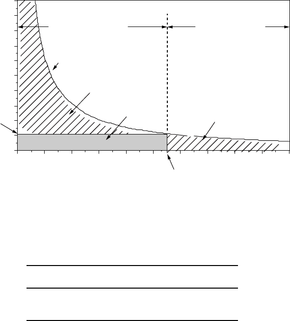
cell. Figure 8.9 uses a plot of (8.2) to illustrate this important concept. The band
gaps for other photovoltaic materials—gallium arsenide (GaAs), cadmium tel-
luride (CdTe), and indium phosphide (InP), in addition to silicon—are shown in
Table 8.2.
These two phenomena relating to photons with energies above and below the
actual band gap establish a maximum theoretical efficiency for a solar cell. To
explore this constraint, we need to introduce the solar spectrum.
8.2.2 The Solar Spectrum
As was described in the last chapter, the surface of the sun emits radiant energy
with spectral characteristics that well match those of a 5800 K blackbody. Just
outside of the earth’s atmosphere, the average radiant flux is about 1.377 kW/m
2
,
an amount known as the solar constant. As solar radiation passes through the
atmosphere, some is absorbed by various constituents in the atmosphere, so that
by the time it reaches the earth’s surface the spectrum is significantly distorted.
The amount of solar energy reaching the ground, as well as its spectral distri-
bution, depends very much on how much atmosphere it has had to pass through
to get there. Recall that the length of the path taken by the sun’s rays through
the atmosphere to reach a spot on the ground, divided by the path length corre-
sponding to the sun directly overhead, is called the air mass ratio,m.Thus,an
BASIC SEMICONDUCTOR PHYSICS 453
2.01.81.61.41.21.00.80.60.40.20.0
9
8
7
6
5
4
3
2
1
0
Photons with not
enough energy
Photons with more
than enough energy
Photon energy,
h
n
Lost energy,
h
n <
E
g
Lost energy,
h
n >
E
g
Photon energy (eV)
Wavelength (µm)
1.11
E
g
= 1.12
Usable energy
SILICON
Figure 8.9 Photons with wavelengths above 1.11 µm don’t have the 1.12 eV needed to
excite an electron, and this energy is lost. Photons with shorter wavelengths have more
than enough energy, but any energy above 1.12 eV is wasted as well.
TA BLE 8.2 Band Gap and Cut-off Wavelength
Above Which Electron Excitation Doesn’t Occur
Quantity Si GaAs CdTe InP
Band gap (eV) 1.12 1.42 1.5 1.35
Cut-off wavelength (µm) 1.11 0.87 0.83 0.92
air mass ratio of 1 (designated “AM1”) means that the sun is directly overhead.
By convention, AM0 means no atmosphere; that is, it is the extraterrestrial solar
spectrum. For most photovoltaic work, an air mass ratio of 1.5, corresponding to
the sun being 42 degrees above the horizon, is assumed to be the standard. The
solar spectrum at AM 1.5 is shown in Fig. 8.10. For an AM 1.5 spectrum, 2%
of the incoming solar energy is in the UV portion of the spectrum, 54% is in the
visible, and 44% is in the infrared.
8.2.3 Band-Gap Impact on Photovoltaic Efficiency
We can now make a simple estimate of the upper bound on the efficiency of a
silicon solar cell. We know the band gap for silicon is 1.12 eV, corresponding to a
wavelength of 1.11 µm, which means that any energy in the solar spectrum with
wavelengths longer than 1.11 µm cannot send an electron into the conduction
band. And, any photons with wavelength less than 1.11 µm waste their extra
energy. If we know the solar spectrum, we can calculate the energy loss due to
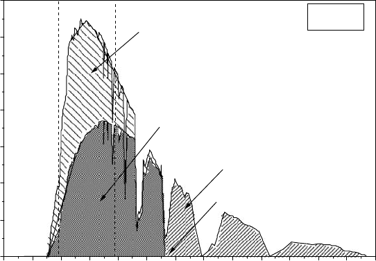
454 PHOTOVOLTAIC MATERIALS AND ELECTRICAL CHARACTERISTICS
2.62.42.22.01.81.61.41.21.00.80.60.40.20.0
0
200
400
600
800
1000
1200
1400
Unavailable energy,
h
n <
E
g
20.2%
Unavailable energy,
h
n >
E
g
30.2%
Energy available, 49.6%
AM 1.5
Radiant power (W/m
2
µm)
Wavelength (µm)
UV 2% Visible 54% IR 44%
Band-gap wavelength
1.11 µm
Figure 8.10 Solar spectrum at AM 1.5. Photons with wavelengths longer than 1.11 µm
don’t have enough energy to excite electrons (20.2% of the incoming solar energy); those
with shorter wavelengths can’t use all of their energy, which accounts for another 30.2%
unavailable to a silicon photovoltaic cell. Spectrum is based on ERDA/NASA (1977).
these two fundamental constraints. Figure 8.10 shows the results of this analysis,
assuming a standard air mass ratio AM 1.5. As is presented there, 20.2% of
the energy in the spectrum is lost due to photons having less energy than the
band gap of silicon (hν < E
g
), and another 30.2% is lost due to photons with
hν > E
g
. The remaining 49.6% represents the maximum possible fraction of
the sun’s energy that could be collected with a silicon solar cell. That is, the
constraints imposed by silicon’s band gap limit the efficiency of silicon to just
under 50%.
Even this simple discussion gives some insight into the trade-off between
choosing a photovoltaic material that has a small band gap versus one with a
large band gap. With a smaller band gap, more solar photons have the energy
needed to excite electrons, which is good since it creates the charges that will
enable current to flow. However, a small band gap means that more photons have
surplus energy above the threshold needed to create hole–electron pairs, which
wastes their potential. High band-gap materials have the opposite combination. A
high band gap means that fewer photons have enough energy to create the current-
carrying electrons and holes, which limits the current that can be generated. On
the other hand, a high band gap gives those charges a higher voltage with less
leftover surplus energy.
In other words, low band gap gives more current with less voltage while high
band gap results in less current and higher voltage. Since power is the product
BASIC SEMICONDUCTOR PHYSICS 455
of current and voltage, there must be some middle-ground band gap, usually
estimated to be between 1.2 eV and 1.8 eV, which will result in the highest
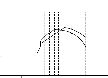
power and efficiency. Figure 8.11 shows one estimate of the impact of band gap
on the theoretical maximum efficiency of photovoltaics at both AM0 and AM1.
The figure includes band gaps and maximum efficiencies for many of the most
promising photovoltaic materials being developed today.
Notice that the efficiencies in Fig. 8.11 are roughly in the 20–25%
range—well below the 49.6% we found when we considered only the losses
caused by (a) photons with insufficient energy to push electrons into the
conduction band and (b) photons with energy in excess of what is needed to
do so. Other factors that contribute to the drop in theoretical efficiency include:
1. Only about half to two-thirds of the full band-gap voltage across the ter-
minals of the solar cell.
2. Recombination of holes and electrons before they can contribute to cur-
rent flow.
3. Photons that are not absorbed in the cell either because they are reflected
off the face of the cell, or because they pass right through the cell, or
because they are blocked by the metal conductors that collect current from
the top of the cell.
4. Internal resistance within the cell, which dissipates power.
8.2.4 The p–n Junction
As long as a solar cell is exposed to photons with energies above the band-
gap energy, hole–electron pairs will be created. The problem is, of course, that
40
30
20
10
0
0 0.5 1.0 1.5 2.0 2.5
Energy eV
Efficiency percent
Ge
CulnSe
2
Si
InP
GaAs
CdTe
AlSb
ZnTe
CdS
GaP
Se
AM0
AM1
Figure 8.11 Maximum efficiency of photovoltaics as a function of their band gap.
From Hersel and Zweibel (1982).
456 PHOTOVOLTAIC MATERIALS AND ELECTRICAL CHARACTERISTICS
those electrons can fall right back into a hole, causing both charge carriers to
disappear. To avoid that recombination, electrons in the conduction band must
continuously be swept away from holes. In PVs this is accomplished by creating
a built-in electric field within the semiconductor itself that pushes electrons in
one direction and holes in the other. To create the electric field, two regions
are established within the crystal. On one side of the dividing line separating
the regions, pure (intrinsic) silicon is purposely contaminated with very small
amounts of a trivalent element from column III of the periodic chart; on the
other side, pentavalent atoms from column V are added.
Consider the side of the semiconductor that has been doped with a pentavalent
element such as phosphorus. Only about 1 phosphorus atom per 1000 silicon
atoms is typical. As shown in Fig. 8.12, an atom of the pentavalent impurity
forms covalent bonds with four adjacent silicon atoms. Four of its five electrons
are now tightly bound, but the fifth electron is left on its own to roam around
the crystal. When that electron leaves the vicinity of its donor atom, there will
remain a +5 donor ion fixed in the matrix, surrounded by only four negative
valence electrons. That is, each donor atom can be represented as a single, fixed,
immobile positive charge plus a freely roaming negative charge as shown in
Fig. 8.12b. Pentavalent i.e., +5 elements donate electrons to their side of the
semiconductor so they are called donor atoms. Since there are now negative
charges that can move around the crystal, a semiconductor doped with donor
atoms is referred to as an “n-type material.”
On the other side of the semiconductor, silicon is doped with a trivalent
element such as boron. Again the concentration of dopants is small, something
on the order of 1 boron atom per 10 million silicon atoms. These dopant atoms fall
into place in the crystal, forming covalent bonds with the adjacent silicon atoms as
shown in Fig. 8.13. Since each of these impurity atoms has only three electrons,
only three of the covalent bonds are filled, which means that a positively charged
hole appears next to its nucleus. An electron from a neighboring silicon atom can
easily move into the hole, so these impurities are referred to as acceptors since
they accept electrons. The filled hole now means there are four negative charges
Free electron
Pentavalent donor
atom
Silicon atoms
+5
+4
+4
+5
+4
+4
+4
+4
+4
=
+
Donor ion
(immobile + charge)
Free electron
(mobile − charge)
(a) The donor atom in Si crystal
(b) Representation of the donor atom
Figure 8.12 An n-type material. (a) The pentavalent donor. (b) The representation of
the donor as a mobile negative charge with a fixed, immobile positive charge.
BASIC SEMICONDUCTOR PHYSICS 457
Movable hole
Trivalent acceptor
atom
Silicon atoms
+3
+4
+4
+3
+4
+4
+4
+4
+4
=
−
+
Acceptor atom
(immobile − charge)
Hole
(mobile + charge)
(a) An acceptor atom in Si crystal
(b) Representation of the acceptor atom
Hole
+
Figure 8.13 In a p-type material, trivalent acceptors contribute movable, positively
charged holes leaving rigid, immobile negative charges in the crystal lattice.
p
n
+
+
+
+
+
+
+
+
+
−
+
−
+
−
+
+
−
+
−
+
−
+
−
+
−
+
p
n
+
+
+
+
+
+
+
+
+
−
+
−
+
−
+
−
+
−
+
−
+
Immobile
negative
charges
Immobile
positive charges
Mobile
holes
Mobile
electrons
Junction
Depletion
region
Electric field
(a) When first brought together (b) In steady-state
−−−
−−−
−−−
−−−
−
−
−−
−−
Figure 8.14 (a) When a p –n junction is first formed, there are mobile holes in the
p-side and mobile electrons in the n-side. (b) As they migrate across the junction, an
electric field builds up that opposes, and quickly stops, diffusion.
surrounding a +3 nucleus. All four covalent bonds are now filled creating a fixed,
immobile net negative charge at each acceptor atom. Meanwhile, each acceptor
has created a positively charged hole that is free to move around in the crystal,
so this side of the semiconductor is called a p-type material.
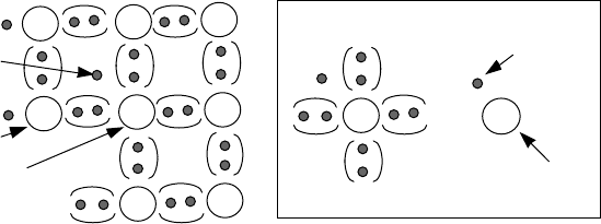
Now, suppose we put an n-type material next to a p-type material forming a
junction between them. In the n-type material, mobile electrons drift by diffusion
across the junction. In the p-type material, mobile holes drift by diffusion across
the junction in the opposite direction. As depicted in Fig. 8.14, when an electron
crosses the junction it fills a hole, leaving an immobile, positive charge behind
in the n-region, while it creates an immobile, negative charge in the p-region.
These immobile charged atoms in the p and n regions create an electric field that
works against the continued movement of electrons and holes across the junction.
As the diffusion process continues, the electric field countering that movement
increases until eventually (actually, almost instantaneously) all further movement
of charged carriers across the junction stops.