Masters G.M. Renewable and Efficient Electric Power Systems
Подождите немного. Документ загружается.

458 PHOTOVOLTAIC MATERIALS AND ELECTRICAL CHARACTERISTICS
The exposed immobile charges creating the electric field in the vicinity of the
junction form what is called a depletion region, meaning that the mobile charges
are depleted—gone—from this region. The width of the depletion region is only
about 1 µm and the voltage across it is perhaps 1 V, which means the field
strength is about 10,000 V/cm! Following convention, the arrows representing
an electric field in Fig. 8.14b start on a positive charge and end on a negative
charge. The arrow, therefore, points in the direction that the field would push
a positive charge, which means that it holds the mobile positive holes in the
p-region (while it repels the electrons back into the n-region).
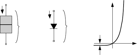
8.2.5 The p–n Junction Diode
Anyone familiar with semiconductors will immediately recognize that what has
been described thus far is just a common, conventional p –n junction diode, the
characteristics of which are presented in Fig. 8.15. If we were to apply a voltage
V
d
across the diode terminals, forward current would flow easily through the
diode from the p-side to the n-side; but if we try to send current in the reverse
direction, only a very small (≈10
−12
A/cm
2
) reverse saturation current I
0
will
flow. This reverse saturation current is the result of thermally generated carriers
with the holes being swept into the p-side and the electrons into the n-side. In
the forward direction, the voltage drop across the diode is only a few tenths
of a volt.
The symbol for a real diode is shown here as a blackened triangle with a bar;
the triangle suggests an arrow, which is a convenient reminder of the direction
in which current flows easily. The triangle is blackened to distinguish it from
an “ideal” diode. Ideal diodes have no voltage drop across them in the forward
direction, and no current at all flows in the reverse direction.
The voltage–current characteristic curve for the p –n junction diode is described
by the following Shockley diode equation:
I
d
= I
0
(e
qV
d
/kT
− 1)(8.3)
p
n
I
d
I
d
I
d
=
I
0
(e
38.9
V
d
− 1)
I
0
I
d
V
d
V
d
V
d
+
−
+
−
+
−
(a)
p
−
n
junction
diode
(b) Symbol for
real diode
(c) Diode characteristic
curve
Figure 8.15 A p –n junction diode allows current to flow easily from the p-side to the
n-side, but not in reverse. (a) p –n junction; (b) its symbol; (c) its characteristic curve.
BASIC SEMICONDUCTOR PHYSICS 459
where I
d
is the diode current in the direction of the arrow (A), V
d
is the voltage
across the diode terminals from the p-side to the n-side (V), I
0
is the reverse sat-
uration current (A), q is the electron charge (1.602 × 10
−19
C), k is Boltzmann’s
constant (1.381 × 10
−23
J/K), and T is the junction temperature (K).
Substituting the above constants into the exponent of (8.3) gives
qV
d
kT
=
1.602 × 10
−19
1.381 × 10
−23
·
V
d
T(K)
= 11, 600
V
d
T(K)
(8.4)
A junction temperature of 25
◦
C is often used as a standard, which results in the
following diode equation:
I
d
= I
0
(e
38.9V
d
− 1)(at 25
◦
C)(8.5)
Example 8.2 A p –n Junction Diode. Consider a p –n junction diode at 25
◦
C
with a reverse saturation current of 10
−9
A. Find the voltage drop across the
diode when it is carrying the following:
a. no current (open-circuit voltage)
b. 1 A
c. 10 A
Solution
a. In the open-circuit condition, I
d
= 0, so from (8.5) V
d
= 0.
b. With I
d
= 1A,wecanfindV
d
by rearranging (8.5):
V
d
=
1
38.9
ln
I
d
I
0
+ 1
=
1
38.9
ln
1
10
−9
+ 1
= 0.532 V
c. with I
d
= 10 A,
V
d
=
1
38.9
ln
10
10
−9
+ 1
= 0.592 V
Notice how little the voltage drop changes as the diode conducts more and
more current, changing by only about 0.06 V as the current increased by a factor
of 10. Often in normal electronic circuit analysis, the diode voltage drop when
it is conducting current is assumed to be nominally about 0.6 V, which is quite
in line with the above results.
While the Shockley diode equation (8.3) is appropriate for our purposes, it
should be noted that in some circumstances it is modified with an “ideality
460 PHOTOVOLTAIC MATERIALS AND ELECTRICAL CHARACTERISTICS
factor” A, which accounts for different mechanisms responsible for moving car-
riers across the junction. The resulting equation is then
I
d
= I
0
(e
qV
d
/AkT
− 1)(8.6)
where the ideality factor A is 1 if the transport process is purely diffusion, and
A ≈ 2 if it is primarily recombination in the depletion region.
8.3 A GENERIC PHOTOVOLTAIC CELL
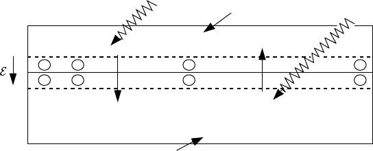
Let us consider what happens in the vicinity of a p –n junction when it is exposed
to sunlight. As photons are absorbed, hole-electron pairs may be formed. If these
mobile charge carriers reach the vicinity of the junction, the electric field in the
depletion region will push the holes into the p-side and push the electrons into
the n-side, as shown in Fig. 8.16. The p-side accumulates holes and the n-side
accumulates electrons, which creates a voltage that can be used to deliver current
to a load.
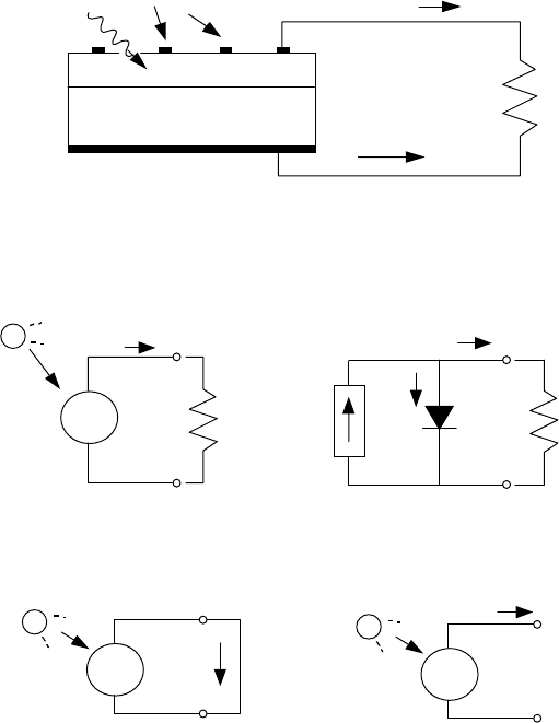
If electrical contacts are attached to the top and bottom of the cell, electrons
will flow out of the n-side into the connecting wire, through the load and back
to the p-side as shown in Fig. 8.17. Since wire cannot conduct holes, it is only
the electrons that actually move around the circuit. When they reach the p-side,
they recombine with holes completing the circuit. By convention, positive current
flows in the direction opposite to electron flow, so the current arrow in the figure
shows current going from the p-side to the load and back into the n-side.
8.3.1 The Simplest Equivalent Circuit for a Photovoltaic Cell
A simple equivalent circuit model for a photovoltaic cell consists of a r eal diode
in parallel with an ideal current source as shown in Fig. 8.18. The ideal current
source delivers current in proportion to the solar flux to which it is exposed.
−
−
+
+
++++++++
Electrons
Holes
Photon
Photon
+ +
− −
+
−
+
−
n
-type
p
-type
−−−−−−
Depletion
region
Accumulated positive charge
Accumulated negative charge
Figure 8.16 When photons create hole–electron pairs near the junction, the electric field
in the depletion region sweeps holes into the p-side and sweeps electrons into the n-side
of the cell.
A GENERIC PHOTOVOLTAIC CELL 461
n
-type
p
-type
Load
I
Photons
V
+
−
Electrical contacts
Bottom contact
Electrons
Figure 8.17 Electrons flow from the n-side contact, through the load, and back to
the p-side where they recombine with holes. Conventional current I is in the oppo-
site direction.
I
d
Load
I
V
+
−
+
−
Load =
I
SC
PV
I
V
+
−
Figure 8.18 A simple equivalent circuit for a photovoltaic cell consists of a current
source driven by sunlight in parallel with a real diode.
+
−
+
−
PV
I
=
I
SC
+
−
PV
V
= 0
I
= 0
V
=
V
OC
(a) Short-circuit current
(b) Open-circuit voltage
Figure 8.19 Two important parameters for photovoltaics are the short-circuit current I
SC
and the open-circuit voltage V
OC
.
There are two conditions of particular interest for the actual PV and for its
equivalent circuit. As shown in Fig. 8.19, they are: (1) the current that flows
when the terminals are shorted together (the short-circuit current, I
SC
) and (2) the
voltage across the terminals when the leads are left open (the open-circuit voltage,
V
OC
). When the leads of the equivalent circuit for the PV cell are shorted together,
no current flows in the (real) diode since V
d
= 0, so all of the current from the
ideal source flows through the shorted leads. Since that short-circuit current must
equal I
SC
, the magnitude of the ideal current source itself must be equal to I
SC
.
Now we can write a voltage and current equation for the equivalent circuit of
the PV cell shown in Fig. 8.18b. Start with
I = I
SC
− I
d
(8.7)
462 PHOTOVOLTAIC MATERIALS AND ELECTRICAL CHARACTERISTICS
and then substitute (8.3) into (8.7) to get
I = I
SC
− I
0
e
qV/kT
− 1
(8.8)
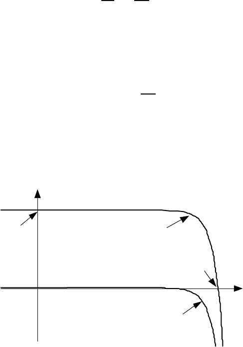
It is interesting to note that the second term in (8.8) is just the diode equation
with a negative sign. That means that a plot of (8.8) is just I
SC
added to the diode
curve of Fig. 8.15c turned upside-down. Figure 8.20 shows the current–voltage
relationship for a PV cell when it is dark (no illumination) and light (illuminated)
based on (8.8).
When the leads from the PV cell are left open, I = 0 and we can solve (8.8)
for the open-circuit voltage V
OC
:
V
OC
=
kT
q
ln
I
SC
I
0
+ 1
(8.9)
And at 25
◦
C, (8.8) and (8.9) become
I = I
SC
− I
0
(e
38.9V
− 1)(8.10)
and
V
OC
= 0.0257 ln
I
SC
I
0
+ 1
(8.11)
In both of these equations, short-circuit current, I
SC
, is directly proportional
to solar insolation, which means that we can now quite easily plot sets of
PV current–voltage curves for varying sunlight. Also, quite often laboratory
specifications for the performance of photovoltaics are given per cm
2
of junction
Dark
Light
I
SC
V
OC
V
I
0
Figure 8.20 Photovoltaic current–voltage relationship for “dark” (no sunlight) and
“light” (an illuminated cell). The dark curve is just the diode curve turned upside-down.
The light curve is the dark curve plus I
SC
.
A GENERIC PHOTOVOLTAIC CELL 463
area, in which case the currents in the above equations are written as current
densities. Both of these points are illustrated in the following example.
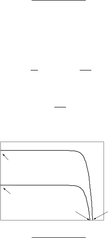
Example 8.3 The I –V Curve for a Photovoltaic Cell. Consider a 100-cm
2
photovoltaic cell with reverse saturation current I
0
= 10
−12
A/cm
2
. In full sun,
it produces a short-circuit current of 40 mA/cm
2
at 25
◦
C. Find the open-circuit
voltage at full sun and again for 50% sunlight. Plot the results.
Solution. The reverse saturation current I
0
is 10
−12
A/cm
2
× 100 cm
2
= 1 ×
10
−10
A. At full sun I
SC
is 0.040 A/cm
2
× 100 cm
2
= 4.0 A. From (8.11) the
open-circuit voltage is
V
OC
= 0.0257 ln
I
SC
I
0
+ 1
= 0.0257 ln
4.0
10
−10
+ 1
= 0.627 V
Since short-circuit current is proportional to solar intensity, at half sun I
SC
= 2
A and the open-circuit voltage is
V
OC
= 0.0257 ln
2
10
−10
+ 1
= 0.610 V
Plotting (8.10) gives us the following:
V
OC
= 0.627 V
V
OC
= 0.610 V
I
SC
= 4 A
I
SC
= 2 A
0.70.60.50.40.30.20.10.0
0.0
0.5
1.0
1.5
2.0
2.5
3.0
3.5
4.0
4.5
Current (A)
Voltage (volts)
Full sun
Half sun
464 PHOTOVOLTAIC MATERIALS AND ELECTRICAL CHARACTERISTICS
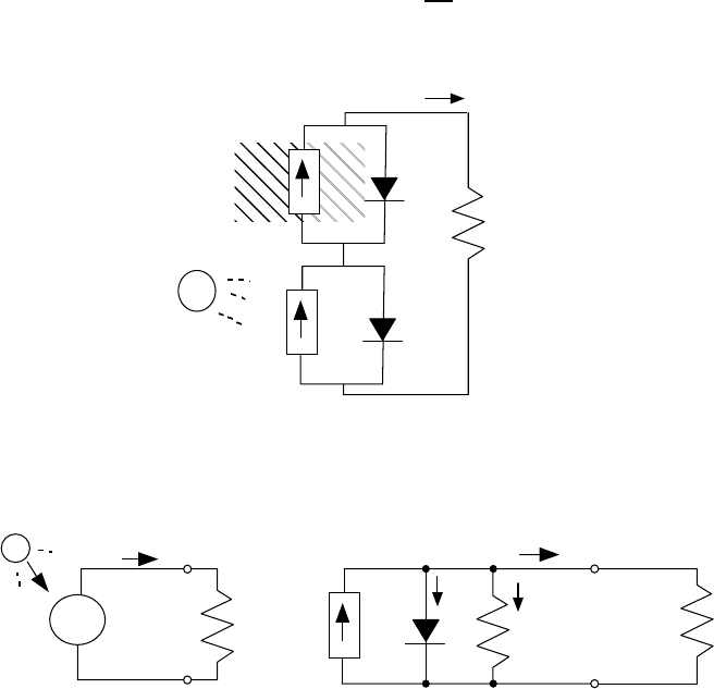
8.3.2 A More Accurate Equivalent Circuit for a PV Cell
There are times when a more complex PV equivalent circuit than the one shown
in Fig. 8.18 is needed. For example, consider the impact of shading on a string of
cells wired in series (Fig. 8.21 shows two such cells). If any cell in the string is in
the dark (shaded), it produces no current. In our simplified equivalent circuit for
the shaded cell, the current through that cell’s current source is zero and its diode
is back biased so it doesn’t pass any current either (other than a tiny amount of
reverse saturation current). This means that the simple equivalent circuit suggests
that no power will be delivered to a load if any of its cells are shaded. While it
is true that PV modules are very sensitive to shading, the situation is not quite
as bad as that. So, we need a more complex model if we are going to be able to
deal with realities such as the shading problem.
Figure 8.22 shows a PV equivalent circuit that includes some parallel leakage
resistance R
p
. The ideal current source I
SC
in this case delivers current to the
diode, the parallel resistance, and the load:
I = (I
SC
− I
d
) −
V
R
p
(8.12)
I
SC
I
= 0
Shaded
cell
Load
I
= 0
Figure 8.21 The simple equivalent circuit of a string of cells in series suggests no
current can flow to the load if any cell is in the dark (shaded). A more complex model
can deal with this problem.
IV
+
−
+
−
Load
PV
I
V
R
P
I
d
Load
I
SC
=
Figure 8.22 The simple PV equivalent circuit with an added parallel resistance.
A GENERIC PHOTOVOLTAIC CELL 465
0.70.60.50.40.30.20.10.0
0.0
0.5
1.0
1.5
2.0
2.5
3.0
3.5
4.0
4.5
Current (amps)
R
P
≠ ∞
∆
I
=
V
/
R
P
R
P
= ∞,
R
S
= 0
slope =
1
R
P
Voltage
Figure 8.23 Modifying the idealized PV equivalent circuit by adding parallel resistance
causes the current at any given voltage to drop by V/R
P
.
I
V
+
−
+
−
Load
PV
I
V
R
S
I
d
V
d
Load
I
SC
=
Figure 8.24 A PV equivalent circuit with series resistance.
The term in the parentheses of (8.12) is the same current that we had for the
simple model. So, what (8.12) tells us is that at any given voltage, the parallel
leakage resistance causes load current for the ideal model to be decreased by
V/R
p
as is shown in Fig. 8.23.
For a cell to have losses of less than 1% due to its parallel resistance, R
P
should be greater than about
R
P
>
100V
OC
I
SC
(8.13)
For a large cell, I
SC
might be around 7 A and V
OC
might be about 0.6 V, which
says its parallel resistance should be greater than about 9 .
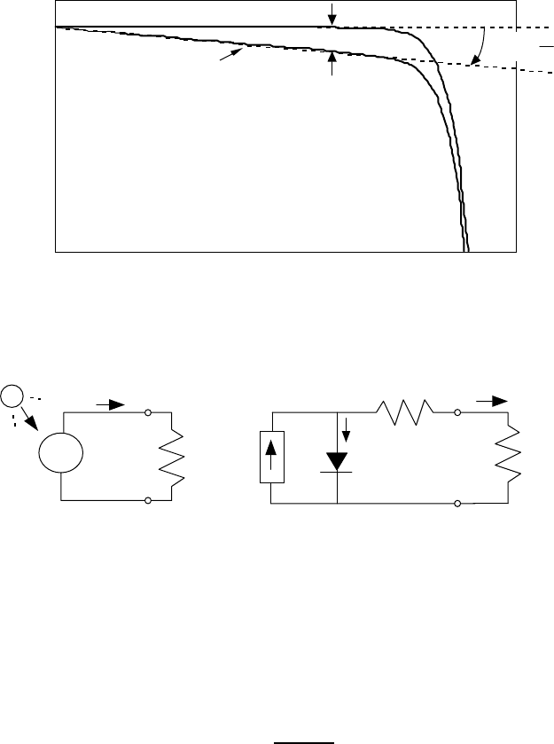
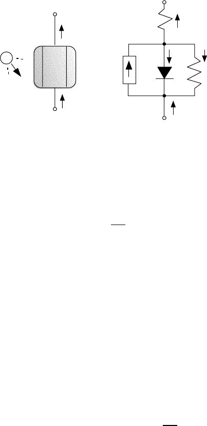
An even better equivalent circuit will include series resistance as well as
parallel resistance. Before we can develop that model, consider Fig. 8.24 in which
the original PV equivalent circuit has been modified to just include some series
resistance, R
S
. S ome of this might be contact resistance associated with the bond
between the cell and its wire leads, and some might be due to the resistance of
the semiconductor itself.
466 PHOTOVOLTAIC MATERIALS AND ELECTRICAL CHARACTERISTICS
To analyze Fig. 8.24, start with the simple equivalent circuit (8.8)
I = I
SC
− I
d
= I
SC
− I
0
e
qV
d
/kT
− 1
(8.8)
and then add the impact of R
S
,
V
d
= V + I · R
S
(8.14)
to give
I = I
SC
− I
0
exp
q(V + I · R
S
)
kT
− 1
(8.15)
Equation (8.15) can be interpreted as the original PV I –V curve with the voltage
at any given current shifted to the left by V = IR
S
as shown in Fig. 8.25.
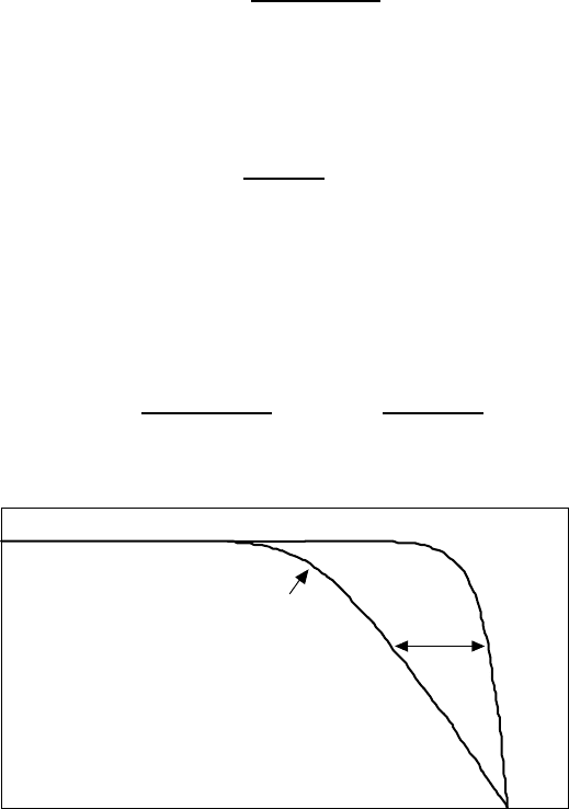
For a cell to have less than 1% losses due to the series resistance, R
S
will
need to be less than about
R
S
<
0.01V
OC
I
SC
(8.16)
which, for a large cell with I
SC
= 7AandV
OC
= 0.6 V, would be less than
0.0009 .
Finally, let us generalize the PV equivalent circuit by including both series and
parallel resistances as shown in Fig. 8.26. We can write the following equation
for current and voltage:
I = I
SC
− I
0
exp
q(V + I · R
S
)
kT
− 1
−
V + I · R
S
R
P
(8.17)
0.70.60.50.40.30.20.10.0
Voltage
0.0
0.5
1.0
1.5
2.0
2.5
3.0
3.5
4.0
4.5
Current (amps)
R
S
≠ 0
∆
V
=
IR
S
R
P
= ∞,
R
S
= 0
Figure 8.25 Adding series resistance to the PV equivalent circuit causes the voltage at
any given current to shift to the left by V = IR
S
.
A GENERIC PHOTOVOLTAIC CELL 467
I
SC
=
PV
R
S
I
I
+
−
V
I
I
V
+
−
Cell
V
d
I
P
R
P
I
d
Figure 8.26 A more complex equivalent circuit for a PV cell includes both parallel and
series resistances. The shaded diode reminds us that this is a “real” diode rather than an
ideal one.
Under the standard assumption of a 25
◦
C cell temperature, (8.17) becomes
I = I
SC
− I
0
e
38.9(V +IR
S
)
− 1
−
1
R
P
(V + IR
S
) at 25
◦
C (8.18)
Unfortunately, (8.18) is a complex equation for which there is no explicit
solution for either voltage V or current I . A spreadsheet solution, however, is
fairly straightforward and has the extra advantage of enabling a graph of I versus
V to be obtained easily. The approach is based on incrementing values of diode
voltage, V
d
, in the spreadsheet. For each value of V
d
, corresponding values of
current I and voltage V can easily be found.
Using the sign convention shown in Fig. 8.26 and applying Kirchhoff’s Cur-
rent Law to the node above the diode, we can write
I
SC
= I + I
d
+ I
P
(8.19)
Rearranging, and substituting the Shockley diode equation (8.5) at 25
◦
Cgives
I = I
SC
− I
0
(e
38.9V
d
− 1) −
V
d
R
P
(8.20)
With an assumed value of V
d
in a spreadsheet, current I can be found from (8.20).
Voltage across an individual cell then can be found from
V = V
d
− IR
S
(8.21)
A plot of (8.18) obtained this way for an equivalent circuit with R
S
= 0.05
and R
P
= 1 is shown in Fig. 8.27. As might be expected, the graph combines
features of Fig. 8.23 and 8.25.