Masters G.M. Renewable and Efficient Electric Power Systems
Подождите немного. Документ загружается.

478 PHOTOVOLTAIC MATERIALS AND ELECTRICAL CHARACTERISTICS
output power by more than half. External diodes, purposely added by the PV
manufacturer or by the system designer, can help preserve the performance of
PV modules. The main purpose for such diodes is to mitigate the impacts of
shading on PV I –V curves. Such diodes are usually added in parallel with
modules or blocks of cells within a module.
8.7.1 Physics of Shading
To help understand this important shading phenomenon, consider Fig. 8.37 in
which an n-cell module with current I and output voltage V shows one cell
separated from the others (shown as the top cell, though it can be any cell in
the string). The equivalent circuit of the top cell has been drawn using Fig. 8.26,
while the other (n − 1) cells in the string are shown as just a module with current
I and output voltage V
n−1
.
In Fig. 8.37a, all of the cells are in the sun and since they are in series, the
same current I flows through each of them. In Fig. 8.37b, however, the top cell
is shaded and its current source I
SC
has been reduced to zero. The voltage drop
across R
P
as current flows through it causes the diode to be reverse biased, so
the diode current is also (essentially) zero. That means the entire current flowing
through the module must travel through both R
P
and R
S
in the shaded cell on its
way to the load. That means the top cell, instead of adding to the output voltage,
actually reduces it.
Consider the case when the bottom n − 1 cells still have full sun and still
some how carry their original current I so they will still produce their original
voltage V
n−1
. This means that the output voltage of the entire module V
SH
with
I
d
R
P
R
P
I
SC
R
S
R
S
n
− 1
cells
.
.
.
.
.
nth
cell
I
I
d
= 0
I
SC
= 0
.
.
.
.
.
nth cell
shaded
(a) All cells in the sun (b) Top cell shaded
I
I
I
I
I
I
I
+
+
−
−
I
V
n
−1
V
n
−1
V
V
SH
n
− 1
cells
Figure 8.37 A module with n cells in which the top cell is in the sun (a) or in the
shade (b).
SHADING IMPACTS ON I–V CURVES 479
one cell shaded will drop to
V
SH
= V
n−1
− I(R
P
+ R
S
)(8.26)
With all n cells in the sun and carrying I, the output voltage was V so the voltage
of the bottom n − 1 cells will be
V
n−1
=
n − 1
n
V(8.27)
Combining (8.26) and (8.27) gives
V
SH
=
n − 1
n
V − I(R
P
+ R
S
)(8.28)
The drop in voltage V at any given current I , caused by the shaded cell, is
given by
V = V − V
SH
= V −
1 −
1
n
V + I(R
P
+ R
S
) (8.29)
V =
V
n
+ I(R
P
+ R
S
) (8.30)
Since the parallel resistance R
P
is so much greater than the series resistance
R
S
, (8.30) simplifies to
V
∼
=
V
n
+ IR
P
(8.31)
At any given current, the I –V curve for the module with one shaded cell drops
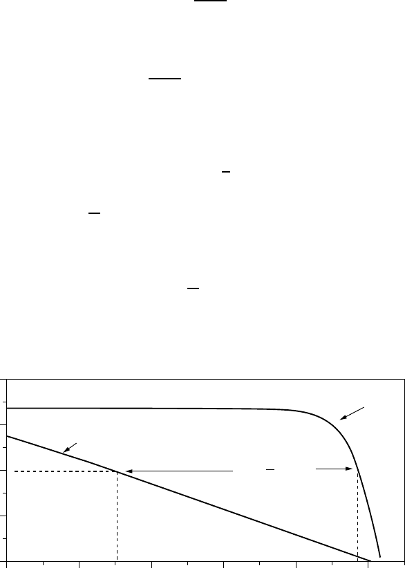
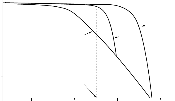
by V . The huge impact this can have is illustrated in Fig. 8.38.
VOLTAGE (V)
CURRENT (A)
∆
V
=
V
n
+
I R
P
I
V
SH
V
I
-
V
one cell shaded
I
-
V
full sun
Figure 8.38 Effect of shading one cell in an n-cell module. At any given current, module
voltage drops from V to V − V .

480 PHOTOVOLTAIC MATERIALS AND ELECTRICAL CHARACTERISTICS
Example 8.6 Impacts of Shading on a PV Module. The 36-cell PV module
described in Example 8.4 had a parallel resistance per cell of R
P
= 6.6 .In
full sun and at current I = 2.14 A the output voltage was found there to be V =
19.41 V. If one cell is shaded and this current somehow stays the same, then:
a. What would be the new module output voltage and power?
b. What would be the voltage drop across the shaded cell?
c. How much power would be dissipated in the shaded cell?
Solution
a. From (8.31) the drop in module voltage will be
V =
V
n
+ IR
P
=
19.41
36
+ 2.14 × 6.6 = 14.66 V
The new output voltage will be 19.41 −14.66 = 4.75 V.
Power delivered by the module with one cell shaded would be
P
module
= VI = 4.75 V × 2.14 A = 10.1W
For comparison, in full sun the module was producing 41.5 W.
b. All of that 2.14 A of current goes through the parallel plus series resistance
(0.005 ) of the shaded cell, so the drop across the shaded cell will be
V
c
= I(R
P
+ R
S
) = 2.14(6.6 + 0.005) = 14.14 V
(normally a cell in the sun will add about 0.5 V to the module; this shaded
cell subtracts over 14 V from the module).
c. The power dissipated in the shaded cell is voltage drop times current,
which is
P = V
c
I = 14.14 V × 2.14 A = 30.2W
All of that power dissipated in the shaded cell is converted to heat, which
can cause a local hot spot that may permanently damage the plastic lami-
nates enclosing the cell.
The procedures demonstrated in Examples 8.4 and 8.6 can be extended to
develop I –V curves under various conditions of shading. Figure 8.39 shows
such curves for the example module under full-sun conditions and with one cell
50% shaded, one cell completely shaded, and two cells completely shaded. Also
shown on the graph is a dashed vertical line at 13 V, which is a typical operating
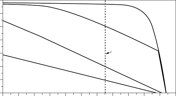
SHADING IMPACTS ON I–V CURVES 481
2220181614121086420
0.0
0.5
1.0
1.5
2.0
2.5
3.0
3.5
VOLTAGE (V)
CURRENT (A)
Full sun
1 cell
shaded 50%
1 cell
shaded 100%
2 cells
shaded 100%
Battery
charging
Figure 8.39 Effects of shading on the I –V curves for a PV module. The dashed line
shows a typical voltage that the module would operate at when charging a 12-V battery;
the impact on charging current is obviously severe.
voltage for a module charging a 12-V battery. The reduction in charging current
for even modest amounts of shading is severe. With just one cell shaded out
of 36 in the module, the power delivered to the battery is decreased by about
two-thirds!
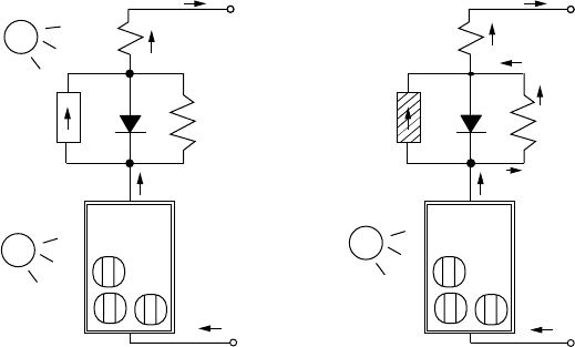
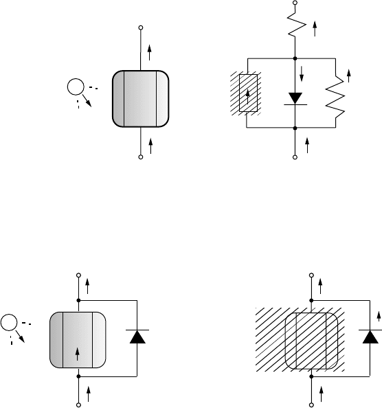
8.7.2 Bypass Diodes for Shade Mitigation
Example 8.6 shows not only how drastically shading can shift the I –V curve,
but also how local, potentially damaging hot spots can be created in shaded
cells. Figure 8.40 shows a typical situation. In Fig. 8.40a a solar cell in full sun
operating in its normal range contributes about 0.5 V to the voltage output of the
module, but in the equivalent circuit shown in 8.40b a shaded cell experiences a
drop as current is diverted through the parallel and series resistances. This drop
can be considerable (in Example 8.6 it was over 14 V).
The voltage drop problem in shaded cells could be to corrected by adding a
bypass diode across each cell, as shown in Fig. 8.41. When a solar cell is in
the sun, there is a voltage rise across the cell so the bypass diode is cut off and
no current flows through it—it is as if the diode is not even there. When the
solar cell is shaded, however, the drop that would occur if the cell conducted any
current would turn on the bypass diode, diverting the current flow through that
diode. The bypass diode, when it conducts, drops about 0.6 V. So, the bypass
diode controls the voltage drop across the shaded cell, limiting it to a relatively
modest 0.6 V instead of the rather large drop that may occur without it.
482 PHOTOVOLTAIC MATERIALS AND ELECTRICAL CHARACTERISTICS
V
c
≈ 0.5 V
I
I
0 V
0 V
I
I
I
V
c
= − (
R
p
+
R
s
)
I
0 A
0 A
R
S
R
P
One cell in the sun
(a) (b)
Equivalent circuit when shaded
Cell
Figure 8.40 In full sun a cell may contribute around 0.5 V to the module output; but
when a cell is shaded, it can have a large voltage drop across it.
I
I
0 A
V
c
≈ 0.5 V V ≈ − 0.6 V
Bypass
diode is
cutoff
I
I
I
Bypass
diode
conducts
Sunny cell Shaded cell
(a) (b)
I
Figure 8.41 Mitigating the shade problem with a bypass diode. In the sun (a), the bypass
diode is cut off and all the normal current goes through the solar cell. In shade (b), the
bypass diode conducts current around the shaded cell, allowing just the diode drop of
about 0.6 V to occur.
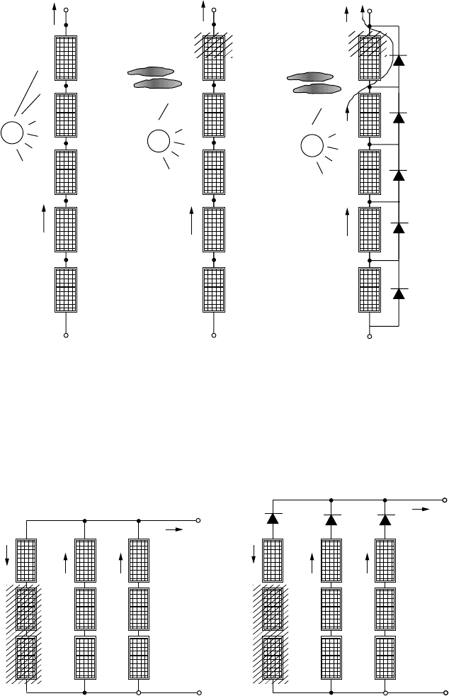
In real modules, it would be impractical to add bypass diodes across every
solar cell, but manufacturers often do provide at least one bypass diode around a
module to help protect arrays, and sometimes several such diodes around groups
of cells within a module. These diodes don’t have much impact on shading
problems of a single module, but they can be very important when a number
of modules are connected in series. Just as cells are wired in series to increase
module voltage, modules can be wired in series to increase array voltage. Also,
just as a single cell can drag down the current within a module, a few shaded
cells in a single module can drag down the current delivered by the entire string
in an array. The benefit already demonstrated for a bypass diode on a single cell
also applies to a diode applied across a complete module.
SHADING IMPACTS ON I–V CURVES 483
To see how bypass diodes wired in parallel with modules can help mitigate
shading problems, consider Fig. 8.42, which shows I –V curves for a string of
five modules (the same modules that were used to derive Fig. 8.39). The graph
shows the modules in full sun as well as the I –V curve that results when one
module has two cells completely shaded. Imagine the PVs delivering charging
current at about 65 V to a 60-V battery bank. As can be seen, in full sun about
3.3 A are delivered to the batteries. However, when just two cells in one module
are shaded, the current drops by one-third to about 2.2 A. With a bypass diode
across the shaded module, however, the I –V curve is improved considerably as
shown in the figure.
Figure 8.43 helps explain how the bypass diodes do their job. Imagine five
modules, wired in series, connected to a battery that forces the modules to oper-
ate at 65 V. In full sun the modules deliver 3.3 A at 65 V. When any of the
cells are shaded, they cease to produce voltage and instead begin to act like
resistors (6.6 per cell in this example) that cause voltage to drop as the other
modules continue to try to push current through the string. Without a bypass
diode to divert the current, the shaded module loses voltage and the other mod-
ules try to compensate by increasing voltage, but the net effect is that current
in the whole string drops. If, however, bypass diodes are provided, as shown
in Fig. 8.43c, then current will go around the shaded module and the charg-
ing current bounces back to nearly the same level that it was before shading
occurred.
Full sun
Shaded,
no bypass
diodes
Shaded,
with
bypass
diodes
Battery
voltage
120100806040200
0.0
0.5
1.0
1.5
2.0
2.5
3.0
3.5
VOLTAGE (V)
CURRENT (A)
Figure 8.42 Impact of bypass diodes. Drawn for five modules in series delivering 65 V
to a battery bank. With one module having two shaded cells, charging current drops by
almost one-third when there are no bypass diodes. With the module bypass diodes there
is very little drop.
484 PHOTOVOLTAIC MATERIALS AND ELECTRICAL CHARACTERISTICS
65 V
80 V
60 V
40 V
20 V
0 V
Partial
shading
Partial
shading
I
= 2.2 A
65 V
On
65.6 V
Off
49.2 V
Off
Off
Off
32.8 V
16.4 V
0 V
I
= 3.2 A
I
= 3.2 A
I
= 2.2 A
(a)
65 V
52 V
39 V
26 V
13 V
0 V
I
= 3.3 A
I
= 3.3 A
Full sun
Partial shading
no bypass diodes
Partial shading
with bypass diodes
(b)
(c)
Figure 8.43 Showing the ability of bypass diodes to mitigate shading when modules
are charging a 65 V battery. Without bypass diodes, a partially shaded module constricts
the current delivered to the load (b). With bypass diodes, current is diverted around the
shaded module.
I
=
I
2
+
I
3
−
I
1
I
=
I
2
+
I
3
V
+
−
Without blocking diodes
I
2
I
2
I
3
I
3
I
1
V
+
−
With blocking diodes
I
1
= 0
(a) (b)
Figure 8.44 Blocking diodes prevent reverse current from flowing down malfunctioning
or shaded strings.
CRYSTALLINE SILICON TECHNOLOGIES 485
8.7.3 Blocking Diodes
Bypass diodes help current go around a shaded or malfunctioning module within a
string. This not only improves the string performance, but also prevents hot spots
from developing in individual shaded cells. When strings of modules are wired
in parallel, a similar problem may arise when one of the strings is not performing
well. Instead of supplying current to the array, a malfunctioning or shaded string
can withdraw current from the rest of the array. By placing blocking diodes (also
called isolation diodes) at the top of each string as shown in Fig. 8.44, the reverse
current drawn by a shaded string can be prevented.
8.8 CRYSTALLINE SILICON TECHNOLOGIES
Thus far, the discussion of photovoltaics has been quite generic; that is, it hasn’t
particularly depended upon what technology was used to fabricate the cells. The
circuit concepts just developed will be used in the next chapter when we explore
PV system design, but before we get there it will be helpful to explore the
different types of technologies currently used to manufacture photovoltaics.
There are a number of ways to categorize photovoltaics. One dichotomy is
based on the thickness of the semiconductor. Conventional crystalline silicon
solar cells are, relatively speaking, very thick—on the order of 200–500 µm
(0.008–0.020 in.). An alternative approach to PV fabrication is based on thin
films of semiconductor, where “thin” means something like 1–10 µm. Thin-film
cells require much less semiconductor material and are easier to manufacture,
so they have the potential to be cheaper than thick cells. The first generation
of thin-film PVs were only about half as efficient as conventional thick silicon
cells; they were less reliable over time, yet they were no cheaper per watt, so
they really weren’t competitive. All three of these negative attributes have been
addressed, more or less successfully, and thin-film PVs are beginning to become
more competitive. In the near future they may even dominate PV sales. Cur-
rently, however, about 80% of all photovoltaics are thick cells and the remaining
20% are thin-film cells used mostly in calculators, watches, and other consumer
electronics.
Photovoltaic technologies can also be categorized by the extent to which atoms
bond with each other in individual crystals. As described by Bube (1998), there is
a “family tree” of PVs based on the size of these crystals. The historically generic
name “polycrystalline” can be broken down into the following more specific
terms: (1) single crystal , the dominant silicon technology; (2) multicrystalline,
in which the cell is made up of a number of relatively large areas of single
crystal grains, each on the order of 1 mm to 10 cm in size, including multicrys-
talline silicon (mc-Si); (3) polycrystalline, with many grains having dimensions
on the order of 1 µm to 1 mm, as is the case for cadmium telluride (CdTe)
cells, copper indium diselenide (CuInSe
2
,) and polycrystalline, thin-film silicon;
(4) microcrystalline cells with grain sizes less than 1 µm; and (5) amorphous,
in which there are no single-crystal regions, as in amorphous silicon (a-Si).
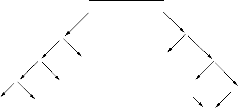
486 PHOTOVOLTAIC MATERIALS AND ELECTRICAL CHARACTERISTICS
Another way to categorize photovoltaic materials is based on whether the p
and n regions of the semiconductor are made of the same material (with dif-
ferent dopings, of course)—for example, silicon. These are called homojunction
photovoltaics. When the p –n junction is formed between two different semi-
conductors, they are called heterojunction PVs. For example, one of the most
promising heterojunction combinations uses cadmium sulfide (CdS) for the n-
type layer and copper indium diselenide (CuInSe
2
, also known as “CIS”) for the
p-type layer.
Other distinctions include multiple junction solar cells (also known as cascade
or tandem cells) made up of a stack of p –n junctions with each junction designed
to capture a different portion of the solar spectrum. The shortest-wavelength,
highest-energy photons are captured in the top layer while most of the rest pass
through to the next layer. Subsequent layers have lower and lower band gaps, so
they each pick off the most energetic photons that they see, while passing the rest
down to the next layer. Very high efficiencies are possible using this approach.
Finally, some cells are specifically designed to work best with concentrated
sunlight while others are used in nonconcentrating flat-plate systems. Figure 8.45
provides a rough road map for our subsequent discussion of each technology.
8.8.1 Single-Crystal Czochralski (CZ) Silicon
Silicon is the second most abundant element on earth, comprising approximately
20% of the earth’s crust. Pure silicon almost immediately forms a layer of SiO
2
on its surface when exposed to air, so it exists in nature mostly in SiO
2
-based
minerals such as quartzite or in silicates such as mica, feldspars, and zeolites.
The raw material for photovoltaics and other semiconductors could be common
sand, but it is usually naturally purified, high-quality silica or quartz (SiO
2
) from
mines. The first processing step to convert silica into crystalline silicon is an
energy-intensive process in which SiO
2
is reduced to an impure Si using carbon
in an arc furnace. It is then transformed to a liquid trichlorosilane (SiHCl
3
),
PHOTOVOLTAICS
Thick Si
200 - 500 µm
Thin films
1 - 10 µm
Multicrystalline Si
30%
Single-crystal Si
Ribbon
Czochralski
CZ
Heterojunction
Multijunction,
Tandem cells
GaAs
InP
CdTe
CIS
Flat-plate
50%
Concentrator
Homojunction
Polycrystalline thin-film Si
Amorphous Si 20%
Figure 8.45 One way to organize the discussion of photovoltaic technologies. Percent-
ages represent fraction of PV sales in the late 1990s.
CRYSTALLINE SILICON TECHNOLOGIES 487
which can be purified by fractional distillation. The purified trichlorosilane can
then be reduced with hydrogen to form extremely pure silicon:
SiHCl
3
+ H
2
+ heat → Si + 3HCl (8.32)
The result is rock-like chunks of 99.9999% pure silicon. When heated to over
1400
◦
C, the rocks can be melted in a quartz crucible to form a molten vat
of silicon.
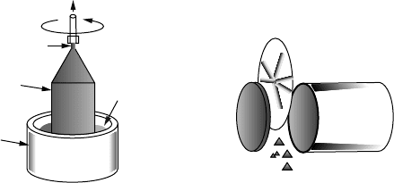
The most commonly used technique for forming single-crystal silicon from the
crucible of molten silicon is the Czochralski, or CZ, method (Fig. 8.46a), in which
a small seed of solid, crystalline silicon about the size of a pencil is dipped into the
vat and then slowly withdrawn using a combination of pulling (10
−4
–10
−2
cm/s)
and rotating (10–40 rpm). As it is withdrawn, the molten silicon atoms bond
with atoms in the crystal and then solidify (freeze) in place. The result is a large
cylindrical ingot or “boule” of single-crystal silicon perhaps a meter long and as
large as about 20 cm in diameter. By adding proper amounts of a dopant to the
melt, the resulting ingot can be fabricated as an n-orp-type material. Usually the
dopant is boron and the ingot is therefore a p-type semiconductor. An alternative
to the Czochralski method is called the float-zone (FZ) process, in which a solid
ingot of silicon is locally melted and then solidified by an RF field that passes
slowly along the ingot.
After the cylindrical ingot is formed, four sides may be sliced off, result-
ing in a block of silicon that has an approximately square cross section. This
“square-ness” allows greater packing density when the cells are assembled into
a photovoltaic module. The silicon block must then be sawed into thin slices
called wafers . This can be done with a saw blade (Fig. 8.46b) or with a diamond
impregnated wire that cuts through the wafer. In either case, a large fraction of
the ingot is lost as kerf (like sawdust)—as much as 50% when a saw blade is
used, less if the wire saw is used. The wafers are then etched to remove some of
the surface damage and to expose the microscopic crystalline structure at the top
of the cell. The surface is made up of a jumble of four-sided pyramids, which
Wafer
Si Ingot
kerf
Seed crystal
Quartz crucible
Molten Si
Crystalline
Si ingot
Saw
Growing the crystal Slicing into wafers
(a) (b)
Figure 8.46 The Czochralski method for growing single-crystal silicon.