Masters G.M. Renewable and Efficient Electric Power Systems
Подождите немного. Документ загружается.

488 PHOTOVOLTAIC MATERIALS AND ELECTRICAL CHARACTERISTICS
helps reflect light down into the crystal. After polishing, the wafers are ready to
be doped to make the p –n junction.
During the above wafer fabrication, the crystalline silicon is usually doped
with acceptor atoms, making it p-type throughout its 200- to- 500-µm thickness.
To form the junction, a thin 0.1- to 0.5-µm n-type layer is created by diffusing
enough donor atoms into the top of the cell to overwhelm the already existing
acceptors. The wafers are placed in long tubes of silica glass for the diffusion
process. The impurities, in gaseous form, flow through the tubes, thereby exposing
the wafers under carefully controlled exposure time and temperature conditions.
For most crystalline silicon, the donor atoms are phosphorus from phosphine gas
(PH
3
) and the acceptors are boron (from diborane, B
2
H
6
).
Since silicon is naturally quite reflective to solar wavelengths, some sort of
surface treatment is required to reduce those losses. An antireflection (AR) coat-
ing of some transparent material such as tin oxide (SnO
2
) is applied. These
coatings tend to readily transmit the green, yellow, and red light into the cell,
but some of the shorter-wavelength blue light is reflected, which gives the cells
their characteristic dark blue color.
The next step is the attachment of electrical contacts to the cell. For many
years, the bottom contacts were formed by vacuum deposition of a layer of
aluminum that covered the back side of the cell. Aluminum is a Group III element,
so it not only serves as a conductor but also can contribute to the concentration of
holes in the bottom of the p-layer, forming what is called a p
+
layer. Those extra
holes help reduce the contact resistance between the silicon and aluminum, and
the gradient of holes that they create helps reduce recombination at the contact
by driving holes away from the back surface. A cross section of a typical 1970s
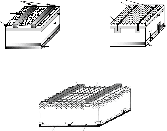
vintage, single-crystal silicon cell is shown in Fig. 8.47a.
The front-surface contacts in most cells have been formed by depositing a
grid of metal conductors that covers on the order of 5–10% of the total area.
That coverage, of course, reduces the amount of sunlight reaching the junction
and hence reduces the overall cell efficiency. Some newer cells, called back-
point contact cells, put both contacts on the bottom to avoid that shading effect.
Another approach involves use of lasers to dig deep, narrow grooves into the
cell. The deep grooves in these laser-grooved, buried-contact cells are filled
with metal, forming a large contact area while minimizing the top-surface area
shaded by the contact. The bottom contacts can also be formed using this laser
technique, resulting in what is called a “double-sided” laser-grooved photovoltaic
cell (Fig. 8.47b).
In newer cells, a number of other techniques may be incorporated into the
top surface to improve performance. One of the most advanced crystalline sili-
con photovoltaics is called the passive-emitter, rear locally diffused (PERL) cell
(Fig. 8.47c). In a PERL cell, inverted pyramids on the front surface, covered with
an antireflection coating, help capture and bounce light into the cell. These cells
not only direct more sunlight into the cell, they also reflect back into the cell
photons that were reflected off of the bottom oxide layer covered by aluminum.
Efficiencies approaching 25% have been achieved.
CRYSTALLINE SILICON TECHNOLOGIES 489
Top metal fingers
Rear metal contact
Antireflection
coating
Surface texturing
p
-type
(a) Conventional 1970s CZ-silicon cell
p
-type
Buried contacts
n
+
layer
p
+
layer
(b) Laser-grooved buried-contact cell
p
+
layer
0.5 µm
p
-layer
200 µm
n
-layer
0.2 µm
Pyramid-shaped
oxide layer
Bottom
contacts
Oxide
Rear
contact
Oxide
Finger
“Inverted”
pyramids
(c) PERL cell
Oxide
p
-silicon
p
+
p
+
p
+
p
+
n
+
Figure 8.47 Evolution of CZ-silicon solar cells. (a) A conventional 1970s cell, showing
typical thicknesses of semiconductor. (b) Double-sided, laser-grooved, buried-contact cell.
(c) Passive-emitter, rear locally diffused (PERL) cell. Based on Green (1993).
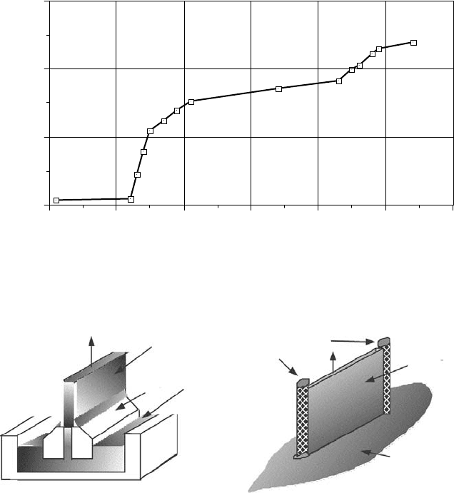
Great progress has been made in improving the maximum efficiency achieved
in laboratory cells. Figure 8.48 illustrates the rise from less than 1% in the 1940s,
to just over 15% in the early 1970s, to over 25% by 2000. Actual production
module efficiencies in 2003 were in the range of 14 to 17%.
8.8.2 Ribbon Silicon Technologies
The fact that the CZ and FZ processes for wafer production were developed
for the semiconductor industry has been both a blessing and a curse. Without
question, the photovoltaics industry has benefited greatly by being able to pig-
gyback onto technology developed for the immense microelectronics industry.
Also, since PVs don’t need the very highest quality wafers, they can use some
of the rejected crystalline silicon originally meant for the semiconductor indus-
try. On the other hand, a wafer that is fabricated into thousands of high-priced
integrated circuits can generate a lot more revenue than one that ends up as a
photovoltaic cell, which means an electronics company can pay a lot more for
wafers, keeping their price high.
With the cost of sliced-and-polished wafers being a significant fraction of the
cost of PVs, attempts have been made to find other ways to fabricate crystalline
490 PHOTOVOLTAIC MATERIALS AND ELECTRICAL CHARACTERISTICS
2000199019801970
Year
196019501940
0
10
20
30
Efficiency (%)
Figure 8.48 Increasing efficiency of single-crystal silicon, laboratory-scale cells. From
Bube (1998).
Crystalline
Si ribbon
Die
Molten Si
Supporting
dendrites
Web crystal
Molten Si
(a) (b)
Figure 8.49 Ribbons of crystalline silicon can be grown using the edge-defined film-fed
growth process (EFG) in (a) or using the dendritic web process (b).
silicon. Several such technologies are based on growing crystalline silicon that
emerges as a long, thin, continuous ribbon from the silicon melt. The ribbons
can then be scribed and broken into rectangular cells without the wastefulness of
sawing an ingot and without the need for separate polishing steps.
One such approach, called “edge-defined, film-fed growth (EFG),” is illus-
trated in Fig. 8.49a. It is based on a carbon die that is partially immersed in
molten silicon. Within the slot-shaped aperture in the die, molten silicon solidifies
and emerges as a frozen ribbon of crystalline silicon. An earlier ribbon process
was based on growth of a thin sheet of crystal between two parallel dendrite sup-
ports (Fig. 8.49b). Very precise temperature control is required for the dendrites,
and the solidifying silicon between them, to form good crystalline material as
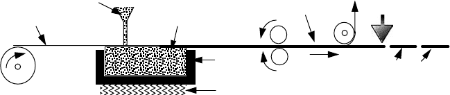
CRYSTALLINE SILICON TECHNOLOGIES 491
Silicon
granulate
feeder
Si melt
Feeding reel
C-fiber net
Heater
Silica
crucible
Pulling
reels
Si ribbon
Carbon net
Cutter
Rectangular cells
Figure 8.50 The S-Web process produces a continuous ribbon of silicon, which can be
doped and cut into individual rectangular cells. Based on Schmela (2000).
the ribbon is pulled from the melt. A similar process is called the String Ribbon
technique, in which two high-temperature vertical strings are pulled vertically
through a shallow silicon melt. The molten silicon spans and freezes between the
strings, forming a long, thin single-crystal ribbon. The silicon ribbon is then cut
to length without interrupting the continuous growth of new ribbon.
A third ribbon technology was introduced by Siemens Solar in 1990, but was
never fully developed until the German company, Brandl AG, picked it up in
2000. The S-Web process utilizes a carbon-fiber net that is pulled horizontally
along the surface of a silicon melt. The silicon solidifies along the lower side of
the net, forming a crystal that can be drawn out into a continuous ribbon, which
can then be doped and cut into rectangular, cell-sized pieces. A sketch of the
process is shown in Fig. 8.50.
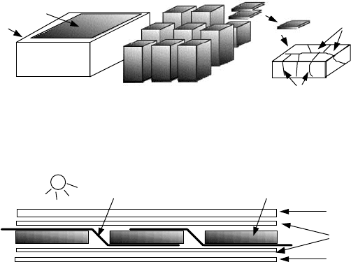
8.8.3 Cast Multicrystalline Silicon
Another way to avoid the costly Czochralski and float-zone processes is based
on carefully cooling and solidifying a crucible of molten silicon, yielding a large,
solid rectangular ingot. Since these ingots may be quite large, on the order of
40 × 40 × 40 cm and weighing over 100 kg, the ingot may need to be cut into
smaller, more manageable blocks, which are then sliced into silicon wafers using
either the saw or wire-cutting techniques. Sawing can waste a significant fraction
of the ingot, but since this casting method is itself cheaper and it utilizes less
expensive, less pure silicon than the CZ process, the waste is less important.
Casting silicon in a mold and then carefully controlling its rate of solidifi-
cation results in an ingot that is not a single, large crystal. Instead, it consists
of many regions, or grains, that are individually crystalline and which tend to
have grain boundaries that run perpendicularly to the plane of the cell. Defective
atomic bonds at these boundaries increase recombination and diminish current
flow, resulting in cell efficiencies that tend to be a few percentage points below
CZ cells. Figure 8.51 illustrates the casting, cutting, slicing, and grain boundary
structure of these multicrystalline silicon (mc-Si) cells.
8.8.4 Crystalline Silicon Modules
The photovoltaic technologies described thus far result in individual thick cells
that must be wired together to create modules with the desired voltage and current
492 PHOTOVOLTAIC MATERIALS AND ELECTRICAL CHARACTERISTICS
Cutting Sawing
Casting
Mold
Si
Wafers
Grains
Grain boundaries
Figure 8.51 Casting, cutting and sawing of silicon results in wafers with individual
grains of crystalline silicon separated by grain boundaries.
Glass
EVA
Interconnecting copper ribbon PV cells
Polymer
+
−
Figure 8.52 Thick crystalline cells must be wired together in series and then sandwiched
in layers of glass, EVA, and polymers for structural support and weather protection.
characteristics. This wiring is done with automated soldering machines, which
connect the cells in series—that is, with the front of one cell connected to the
back of the next, as shown in Fig. 8.52. After soldering, the cells are laminated
into a sandwich of materials that offer structural support as well as weather
protection. The upper surface is tempered glass, and the cells are encapsulated
in two layers of ethylene vinyl acetate (EVA). Finally, the back is covered with
sheets of polymer that prevent moisture penetration.
8.9 THIN-FILM PHOTOVOLTAICS
Conventional crystalline silicon technologies (x-Si) require considerable amounts
of expensive material with additional complexity and costs needed to wire indi-
vidual cells together. Competing technologies, however, are based on depositing
extremely thin films of photovoltaic materials onto glass or metal substrates.
Thin-film devices use relatively little material (their thickness is in the micron
range rather than the hundreds-of-microns range needed by crystalline silicon),
∗
they do not require the complexity of cell interconnections, and they are partic-
ularly well suited to mass-production techniques. Their thinness allows photons
that aren’t absorbed to pass completely through the photovoltaic material, which
offers two special opportunities. Their semitransparency means that they can
be deposited onto windows, making building glass a provider of both light and
∗
For comparison, a human hair is roughly 100 µm in diameter.
THIN-FILM PHOTOVOLTAICS 493
electricity. They also lend themselves to multiple-junction, tandem cells in which
photons of different wavelengths are absorbed in different layers of the device.
In exchange for these highly desirable properties, thin-film cells are not as
efficient as x-Si—especially when they are not used in tandem devices. While
the likelihood of significant reductions in module costs are modest for conven-
tional crystalline silicon, many opportunities remain to increase efficiency and
dramatically reduce costs using thin-film technologies. Many believe that thin
films will be the dominant photovoltaic technology in the future.
8.9.1 Amorphous Silicon
Almost all of today’s thin-film technology is based on amorphous (glassy) silicon
(a-Si)—that is, silicon in which there is very little order to the arrangement of
atoms. Since it is not crystalline, the organized tetrahedral structure in which one
silicon atom bonds to its four adjacent neighbors in a precisely defined manner
does not apply. While almost all of the atoms do form bonds with four other
silicon atoms, there remain numerous “dangling bonds” where nothing attaches
to one of the valence electrons. These dangling-bond defects act as recombination
centers so that photogenerated electrons recombine with holes before they can
travel very far. The key to making a-Si into a decent photovoltaic material was
first discovered, somewhat by accident, in 1969, by a British team that noted a
glow when silane gas SiH
4
was bombarded with a stream of electrons (Chittick
et al., 1969). This led to their critical discovery that by alloying amorphous
silicon with hydrogen the concentration of defects could be reduced by about
three orders of magnitude. The concentration of hydrogen atoms in these alloys
is roughly 1 atom in 10, so their chemical composition is approximately Si
0.9
H
0.1
.
Moreover, the silicon–hydrogen alloy that results, designated as a-Si:H, is easily
doped to make n-type and p-type materials for solar cells.
∗
The first a-Si:H solar cells were describe d in the literature in 1976 (Carlson
and Wronski, 1976). While only 1% efficient, their potential was quickly recog-
nized. The first commercial use of a-Si:H came in 1980 when Sanyo introduced
a line of solar-powered pocket calculators. And by the mid-1980s, amorphous
silicon PV modules for use outdoors were on the market. Their efficiency was
only about 5% or 6% when new; within the first few months of use, this dropped
to about 3% or 4%. Understanding this efficiency instability, and dealing with
it, has remained a significant challenge. By the early 1990s, single-junction cells
had stabilized efficiencies of about 10%, while considerably higher efficiencies
have been reached for multijunction cells.
So, how can a p –n junction be formed in an amorphous material with very
little organization among its atoms? Figure 8.53 shows a cross section of a simple
a-Si:H cell that uses glass as the supporting superstrate. On the underside of the
∗
It is interesting to note that amorphous silicon is finding application in other products besides
photovoltaics. The fact that it is an insulator in the dark but readily conducts current when exposed
to light has led to its incorporation in photoelectronic products such as photocopiers, laser printers,
and fax machines.
494 PHOTOVOLTAIC MATERIALS AND ELECTRICAL CHARACTERISTICS
Glass superstrate
SiO
2
buffer layer
Transparent conducting oxide
p
-layer
Intrinsic (undoped)
a
-Si:H
n
-layer
Aluminum back contact
≈ 60 − 500 nm
≈ 10 nm
≈ 500 nm
≈ 20 nm
≈ 200 nm
≈ 20 nm
2,000,000 nm
Internal electric field
Solar input
hn
−−−
+
++
Figure 8.53 Cross section of an amorphous silicon p –i –n cell. The example thicknesses
are in nanometers (10
−9
m) and are not drawn to scale.
glass a buffer layer of SiO
2
may be deposited in order to prevent subsequent lay-
ers of atoms from migrating into the glass. Next comes the electrical contact for
the top of the cell, which is usually a transparent conducting oxide (TC) such as
tin oxide, indium–tin oxide, or zinc oxide. The solar cell itself is often formed by
subjecting gaseous silicon in the form of silane SiH
4
(or disilane Si
2
H
6
) to bom-
bardment by a stream of electrons. The bombardment creates reactive silane rad-
icals, which can attach themselves onto what becomes a growing layer of amor-
phous silicon. During this process, the excited silane can emit photons of light,
in what is called a glow discharge. The n-layer is formed by adding phosphene
gas PH
3
to the mix, while diborane gas B
2
H
6
is used to form the p-layer.
The actual p –n junction, whose purpose is of course to create the internal
electric field in the cell to separate holes and electrons, consists of three layers
consisting of the p-layer and n-layers separated by an undoped (intrinsic) region
of a-Si:H As shown, the p-layer is only 10 nm thick; the intrinsic layer, or i-
layer, is 500 nm; and the n-layer is 20 nm. Notice that the electric field created
between the rigid positive charges in the n-layer and the rigid negative charges in
the p-layer spans almost the full depth of the cell. This means that light-induced
hole–electron pairs created almost anywhere within the cell will be swept across
the intrinsic layer by the internal field. These amorphous silicon PVs are referred
to as p –i –n cells.
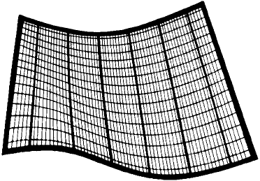
A variation on the a-Si p –i –n cell uses a thin, flexible stainless steel sub-
strate located at the bottom of the cell instead of the glass superstrate shown
in Fig. 8.53. The stainless steel provides the mechanical strength needed while
its flexibility allows modules of these cells to be literally rolled up and stored
(Fig. 8.54). These flexible modules are often fitted with grommets so they can
be lashed to irregular surfaces such as those found on boats.
THIN-FILM PHOTOVOLTAICS 495
Figure 8.54 Flexible a-Si modules can be rolled up and stored when not in use. From
SERI (1985).
The theoretical maximum efficiency for single-junction a-Si is 28%. The best
laboratory cells today have a stabilized efficiency of just over 13 percent but
commercial modules have stabilized efficiencies of only 5 to 8%.
Amorphous Silicon Processing. An important advantage of thin-film photo-
voltaics over conventional crystalline silicon is the ease with which they can be
manufactured. Starting with rather ordinary glass, layer upon layer of materials
are deposited onto the glass in a decomposition chamber. The raw materials are
gaseous rather than solid, and whole modules (many cells connected in series)
are created at one time rather than separately fabricating individual cells that
must be soldered together to form a module.
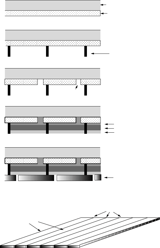
A simplified step-by-step a-Si manufacturing process is described in Fig. 8.55.
It begins with the deposition of a transparent conductor covering the entire under-
side of the glass superstrate (not shown is an SiO
2
buffer layer that might also
be included). Then long narrow metal “stitch” bars, which run the length of the
module, are printed onto the transparent conductor. After scribing the transparent
conductor, the bars will connect the top of one cell to the bottom of the next one.
Now the three layers of silicon are deposited, forming the p –i –n structure of the
cell itself. The final layer to be deposited is the bottom conductor, which is then
scribed with long, narrow cuts that run the length of the module to complete the
separation of one cell from the next. The bottom conductor may be a transparent
oxide or it may be metal. If it is a transparent oxide, then photons that aren’t
captured in the cells can pass through the entire system, delivering some light to
whatever is beneath the module.
Figure 8.56 shows how the individual cells run the entire length of the module
with scribe lines that separate each cell from adjacent cells.
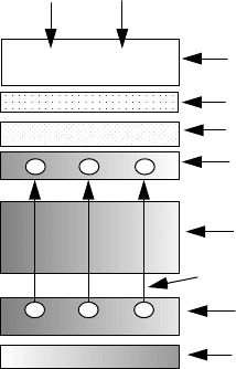
Multijunction or Tandem a-Si The band gap of a-Si:H is 1.75 eV, which
is quite a bit higher than the 1.12 eV for crystalline silicon. Recall that higher
band gaps increase voltage at the expense of lower currents (a smaller fraction of
496 PHOTOVOLTAIC MATERIALS AND ELECTRICAL CHARACTERISTICS
Glass
Transparent conductor
1. Deposit transparent conductor on glass
2. Deposit metallic stitch bars
3. Scribe transparent conductor
4. Deposit
p
−
i
−
n
layers
5. Deposit and scribe back conductors
Stitch bars to
connect cells
Glass
Transparent conductor
Glass
Transparent conductor
Glass
Transparent conductor
Cuts
p
i
n
p
i
n
Glass
Transparent conductor
Back conductors
Figure 8.55 The sequence of steps taken to create a module of amorphous silicon cells.
Linear cells
Scribe lines
Figure 8.56 Individual cells can run the entire length of an amorphous silicon module.
solar photons have sufficient energy to create hole–electron pairs). Since power
is the product of voltage and current, there will be some optimum band gap for
a single-junction cell, which will theoretically result in the most efficient device.
As was shown in Fig. 8.11, that optimum band gap (at AM1 corresponding to
the sun directly overhead) is about 1.4 eV. Thus crystalline silicon has a band
THIN-FILM PHOTOVOLTAICS 497
gap somewhat too low, while a-Si has one too high to be optimum. As it turns
out, however, amorphous silicon has the handy property that alloys made with
other Group IV elements will cause the band gap to change. As a general rule,
moving up a row in the Periodic Table increases band gap, while moving down
a row decreases band gap. Referring to the portion of the Periodic Table given in
Table 8.1, this rule would suggest that carbon (directly above silicon) would have
a higher band gap than silicon, while germanium (directly below silicon) would
have a lower band gap. To lower the 1.75-eV band gap of amorphous silicon
toward the 1.4 eV optimum suggests that an alloy of silicon with the right amount
of germanium (forming a-Si:H:Ge) can help improve cell efficiency. And that
is the case.
The above discussion on a-Si alloys leads to an even more important oppor-
tunity, however. When a-Si is alloyed with carbon, for example, the band gap
can be increased (to about 2 eV), and when alloyed with germanium the gap
will be reduced (to about 1.3 eV). That suggests that multijunction photovoltaic
devices can be fabricated by layering p –n junctions of different alloys. The idea
behind a multijunction cell is to create junctions with decreasing band gaps as
photons penetrate deeper and deeper into the cell. As shown in Fig. 8.57a, the
top junction should capture the most energetic photons while allowing photons
with less energy to pass through to the next junction below, and so forth. In
Fig. 8.57b, an example amorphous silicon, three-junction photovoltaic device is
shown in which advantage is taken of the ability of germanium and carbon to
increase or decrease the a-Si:H band gap.
The theoretical maximum efficiency of an ideal multijunction a-Si:H cell is
42%, and some estimate a practically achievable efficiency of about 24% (Carlson
and Wagner, 1993). By the turn of the century, multijunction, amorphous silicon
modules had a stabilized efficiency of almost 11%.
Glass superstrate
SiO
2
buffer layer
Transparent conductor
Metal back contact
High-energy photons
Medium
energy
Low energy
High band gap
Medium band
gap
Low band
gap
p
i
n
p
i
n
p
i
n
a
-Si
a
-Si:Ge
a
-Si:C
(a)
(b)
a
-Si:C
a
-Si
a
-Si:Ge
Figure 8.57 Multijunction amorphous silicon solar cells can be made by alloying a-Si:H
(band gap ≈1.75 eV) with carbon a-Si:C in the top layer (≈2.0 eV) to capture the high-
est-energy photons and germanium a-Si:Ge (≈1.3 eV) in the bottom layer to capture the
lowest-energy photons.