Moulson A.J., Herbert J.M. Electroceramics: Materials, Properties, Applications
Подождите немного. Документ загружается.

preferentially between 750 and 850 8C whilst perovskite-type structures are formed
between 850 and 950 8C. A processing route bypassing the formation of pyrochlore
has been developed for PMN [23]; MgO is pre-reacted with the Nb
2
O
5
to form
MgNb
2
O
6
which is then reacted with PbO to form the perovskite phase.
A composition approximating to Pb
0.85
La
0.1
Ti
0.2
Zr
0.8
O
3
(e
r
2000) is only
significantly affected by d.c. fields above 2 MV m
71
, as shown in Fig. 5.48. A
number of factors contribute to the stability:
1. the grain size (about 1 mm),
2. the relaxor characteristics,
3. a possible antiferroelectric structure between 735 and +65 8C and
4. T
c
at 70 8C due to the combined effects of the zirconium and lanthanum
contents.
Factor 3 may account for the maintenance of the e
r
level at low temperatures
and the small effect of d.c. fields up to 60 8C, and 1 and 2 contribute to a
322 DIELECTRICS AND INSULATORS
Fig. 5.47 Effect of d.c. bias (MV m
71
) on the dielectric properties of PbFe
0.55
W
0.1
Nb
0.35
O
3
.
TEAMFLY
Team-Fly
®
smoothing out of the peaks which might otherwise occur at 740 and +70 8C.
Factor 2 has the marginal disadvantage of introducing frequency dependence of
e
r
and tan d below 0 8C. Tan d measured at 100 kHz rises to above 0.04 at
720 8C.
The composition sinters at 1100 8C which allows some reduction in the
palladium content of the Ag–Pd electrodes and reduces the volatility of PbO. The
resistivity is very high, leading to a leakage time constant greater than 10
6
sat
room temperature and about 10
5
s at 125 8C. There are very few signs of
degradation under high d.c. fields up to 150 8C.
The La
3+
ion has r
12
¼132 pm and r
6
¼106 pm and appears to be able to
occupy either A or B sites, although a higher lead content may be needed to give
appreciable B-site occupancy. The high resistivity and resistance to degradation
may be due to the lowering of the concentration of vacant oxygen sites by the
replacement of Pb
2+
by La
3+
, accompanied by La
3+
on B sites acting as
acceptors for electrons and compensating the La
3+
ions on A sites.
5.7.3 Multilayer capacitors with base metal electrodes (BME)
The multilayer structure discussed in Section 5.4.3 is applicable to all ceramic
dielectrics. It enables the thinnest dielectric plates to be engineered into robust
units that are readily attached to the substrates carrying the electronic circuitry
by ‘surface mount technology’ (SMT). The structure also gives minimum
electrode inductance permitting use at high frequencies. Very significant progress
has been made over the years in reducing the thickness of both dielectric and
electrode layers and so increasing volumetric efficiency. An appreciable part of
the cost of a multilayer capacitor lies in the palladium-containing electrodes.
HIGH-PERMITTIVITY CERAMICS 323
Fig. 5.48 Dependence of e
r
on T and d.c. bias (——, 0; - - - -, 2 MV m
71
; ---- ----, 4 MV m
71
)
for Pb
0.85
La
0.1
Ti
0.2
Zr
0.8
O
3
(PLZT). (After G.H. Maher (1983) 33rd Electron. Comp. Conf.
(IEEE) 173–7.)
With reductions in ceramic sintering temperature, the cost of electrodes has
been reduced by the use of Ag–Pd alloys, typically 70 at.% Ag/30 at.% Pd. The
reduction in palladium content is limited to about 15 at.% because at lower levels
silver migration becomes a problem. The drive to lower cost has led to efforts to
avoid it entirely. One approach is based upon the ‘injected’ or ‘fugitive’ electrode
(see Section 5.4.3 and Fig. 5.12) and the other on the use of the base metals nickel
or copper for the electrodes (BME) combined with dielectrics resistant to the
reduction firing necessary to retain the electrodes in the metallic state.
Although the fugitive electrode approach is viable it is presently little used, if
at all. In contrast BME technology presently accounts for about 50% of MLCC
production.
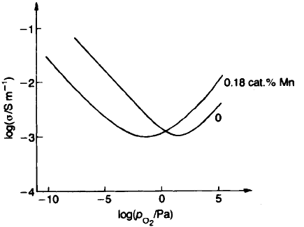
When BaTiO
3
is fired under reducing conditions oxygen is lost from the lattice
with the formation of doubly ionized oxygen vacancies and electrons in the
conduction band (see Section 2.6.2, Eq. (2.48)). On cooling to room temperature
a large fraction of the electrons may remain in the conduction band because the
ionization energies of V
O
and V
.
O
are low compared to kT at room temperature
(see Fig. 2.15). Acceptor ions such as Mn
3+
on Ti
4+
sites also give rise to oxygen
vacancies but without the liberation of electrons. They have the effect of shifting
the minimum in the conductivity–oxygen pressure relation to lower oxygen
pressures (Fig. 5.49) so that the concentration of electrons in the conduction
band is reduced and positive holes in the valence band become the majority
carriers at oxygen pressures above 0.01 Pa (Eq. (2.53)). On cooling to room
temperature the positive holes combine with the ionized acceptors since the
ionization energies for acceptors lie in the range 1–2 eV. High-resistivity BaTiO
3
therefore requires both a sufficient concentration of acceptors and a sufficient
pressure of oxygen during firing.
Technical BaTiO
3
normally contains sufficient acceptors in the form of Al, Fe
etc. to render it insulating after firing at atmospheric pressure, but it requires
324 DIELECTRICS AND INSULATORS
Fig. 5.49 Effect of Mn
0
Ti
on the conductivity–oxygen pressure relation for BaTiO
3
at 965 8C.
additional acceptors if it is to be sintered at lower oxygen pressures. The addition
of 0.2–0.5 mol.% Mn forms sufficient Mn
2+
and Mn
3+
acceptor ions on Ti
4+
sites on firing at oxygen pressures below 10
72
Pa to result in an insulating
dielectric at room temperature.
The oxidation reaction for nickel is
Ni þ
1
2
O
2
ðgÞ!NiO ð5:46Þ
and the standard free-energy change at 1300 8C(DG
0
at 1573 K) is approximately
7100 kJ. If the activities of Ni and NiO are set equal to unity, the reaction
constant K is
K ¼ p
O
2
1=2
ð5:47Þ
and since DG
0
1573
¼RT lnK ¼RT lnp
O
2
1=2
,
p
O
2
¼ exp
2DG
0
1573
RT
ð5:48Þ
2.5 10
7
bar ð10
2
PaÞ
The oxygen potential must be kept below this value at the firing temperature
(about 1300 8C) if the nickel electrodes are to remain metallic. This is achieved by
firing in nitrogen carrying a controlled H
2
O/H
2
mixture. An oxygen meter (see
Section 4.6.1) is used to monitor the oxygen potential in the firing zone.
HIGH-PERMITTIVITY CERAMICS 325
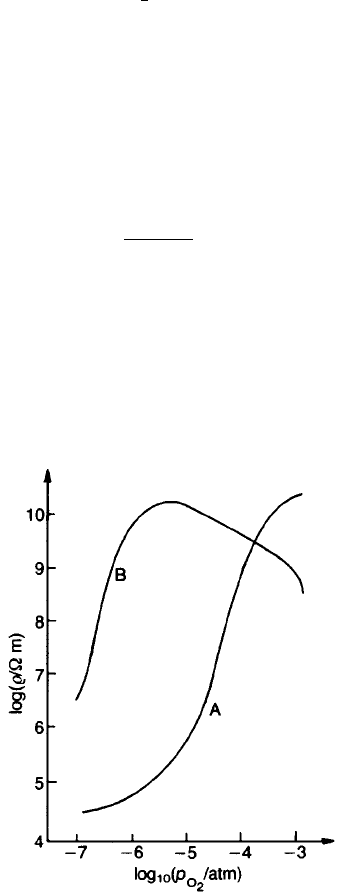
Fig. 5.50 Resistivity at room temperature as a function of oxygen pressure during sintering:
curve A, undoped BaTi
0.85
Zr
0.15
O
3
; curve B, (Ba
0.85
Ca
0.15
O)
1.01
–(Ti
0.9
Zr
0.1
)O
2
. (After [24])
The titanate can also be stabilized against reduction by the substitution of some
calcium for barium, and by establishing the ratio AO/BO
2
41. A suitable
composition is [(Ba
0.85
Ca
0.15
)O]
1.01
(Ti
0.9
Zr
0.1
)O
2
, and its stability against firing
under reducing conditions is compared with that for Ba(Ti
0.85
Zr
0.15
)O
3
in Fig. 5.50
[24].
The success of the formulation is probably due to the presence of Ca
2+
ions on
B sites acting as acceptors (Section 5.7.1). Certainly an AO/BO
2
ratio greater than
unity has been found to be essential. CaZrO
3
is itself very resistant to reducing
conditions, and the presence of Ca and Zr ions will confer some measure of
increased resistance to reduction on the composition as a whole. The loss of lattice
oxygen resulting from the reduction firing, unless compensated for, has the
expected adverse effect upon degradation of BME MLCCs and the need to
control this has stimulated research into what is undoubtedly a very complex
matter.
The BME process cannot be applied to compositions containing lead because
of the ease of reduction to metallic lead.
5.7.4 Barrier-layer capacitors (Class IV)
Although barrier layer capacitors are of little or no commercial significance, the
principles upon which their manufacture and operation are based, are important.
Most materials containing TiO
2
, whether as a single phase or in combination
with other oxides, become conductive on firing in reducing atmospheres. The
ease of reduction is strongly affected by the other ions present: acceptor ions tend
to inhibit reduction and donor ions tend to enhance it. In most cases a high
resistivity can be restored by annealing in air or oxygen. The mechanism of
conduction is discussed in Section 2.6.2.
Barrier-layer capacitors are based on the limited reoxidation of a reduced
composition. This results, in the simplest case, in a surface layer of high
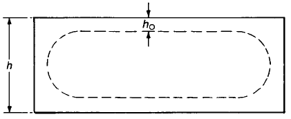
resistivity and a central portion of conductive material so that the effective
dielectric thickness is twice the thickness h
o
of a single reoxidized layer and there
is an apparent gain in permittivity over that of a fully oxidized unit by a factor of
h/2h
o
, where h is the overall dielectric thickness (Fig. 5.51). Alternatively each
326 DIELECTRICS AND INSULATORS
Fig. 5.51 Schematic diagram of a partially reoxidized dielectric.
conductive grain may be surrounded by an insulating barrier layer so that the
dielectric property is dispersed throughout the ceramic.
Reoxidized layer units
Units depending on a reoxidized surface layer are generally made by firing
BaTiO
3
or SrTiO
3
discs, approximately 0.5 mm thick, under reducing conditions.
A silver electrode paint is applied to the surfaces of the disc and fired on at about
800 8C. The silver paint contains a PbO–Bi
2
O
3
–B
2
O
3
glass frit to which is added a
small amount (about 1 cat.%) of acceptor ions, e.g. Cu. This leads to the
formation of a thin (about 10 mm) insulating layer separating the electrodes from
the semiconducting titanate and to an associated very high capacitance. Because
the major part of a voltage applied to the capacitor is dropped across the two
thin dielectric layers, the working voltage is low, typically about 10 V.
Capacitance values per unit electrode area of approximately 10 mF m
72
are
readily achieved.
Internal barrier layers
The thinnest reoxidized layers, which result in very large effective permittivities,
have properties similar in some respects to those of varistors as described in
Section 4.3. They contain Schottky barriers in the semiconducting surfaces of the
grains which result in properties similar to those of two back-to-back diodes (see
Fig. 2.22). Their working voltages are therefore limited to the range within which
the current is low. In order to withstand higher voltages it is necessary to have a
ceramic structure that comprises a number of such barrier layers in series
between the electrodes. There must also be an intergranular component that
allows the diffusion of oxygen and dopant ions to the crystallite surfaces during
oxidation.
The grain size in these units averages about 25 mm. Crystallites smaller than
about 10 mm have a large fraction of their volume taken up by Schottky barriers
and associated space charges that increase their resistivity, and if the crystals are
larger than 50 mm there is the possibility that only a few crystals will separate the
electrodes in some places, resulting in a greater likelihood of breakdown.
Additions of small amounts (about 1%) of silica and alumina provide an
intergranular layer that allows ionic movement and access to oxygen at high
temperatures. Dysprosium or other donor ions are added to assist in the
reduction process.
Discs or other shapes are first fired in air to remove organic matter and then
sintered in air to obtain the required level of crystal growth. A reducing
atmosphere of carbon monoxide or hydrogen is then introduced. This is found to
HIGH-PERMITTIVITY CERAMICS 327
inhibit crystal growth and so cannot usually be combined with the sintering stage.
After cooling, a boric oxide frit containing acceptor ions such as Cu, Mn, Bi or Tl is
painted on the surfaces of the pieces which are then reheated in air to 1300–
1400 8C. The acceptor ions diffuse along the grain boundaries and modify the
surface properties of the crystallites in much the same way as the acceptors that
protect dielectrics for base-metal-electroded multilayer capacitors. However, their
precise behaviour has not been established since it is extremely difficult to
determine the structure of the thin intergranular layers and their interfaces with the
crystallites.
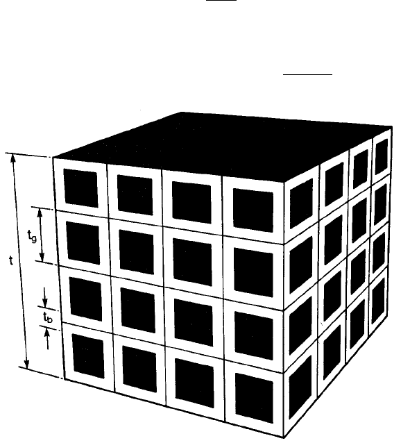
Model calculations
The structure of internal-barrier-layer units can be represented by the simplified
model shown in Fig. 5.52. The overall capacitance can be calculated as follows.
The capacitance C
i
of an individual element, assuming t
g
t
b
, is given by
C
i
¼
e
r
e
0
t
2
g
t
b
ð5:49Þ
and that of a series connected column by
C
i
=ðno. of elements in columnÞ¼
e
r
e
0
t
2
g
=t
b
t=t
g
ð5:50Þ
328 DIELECTRICS AND INSULATORS
Fig. 5.52 Schematic diagram of a section through an internal-barrier-layer capacitor.

The capacitance C per unit area is
C ¼
e
r
e
0
t
g
tt
b
ð5:51Þ
since there are 1/t
g
2
columns per unit area. It follows that the effective relative
permittivity e
re
of the composite dielectric is
e
re
¼
e
r
t
g
t
b
ð5:52Þ
Assuming t
g
¼ 50 mm, t
b
¼ 0.2 mm and e
r
¼ 200, we obtain e
re
¼ 50 000. Values
as high as this can be achieved in practice with tan d values of typically 0.03.
Units based on SrTiO
3
are more stable with respect to field and temperature
than those based on BaTiO
3
. Their capacitance is only reduced by 5% under
maximum d.c. field and their variation with temperature can be kept within
+20% over a 720 to +85 8C range; their effective permittivity is 10 000–20 000.
BaTiO
3
units have effective permittivities of up to 50 000.
5.7.5 Ferroelectric memories
No text covering electroceramics can omit some discussion of ‘ferroelectric
memories’ even though the engineering of the ceramics into the memory elements
of a computer is so highly specialized that it is arguably more properly dealt with
in the context of semiconductor technologies. Certainly the topic demonstrates
very clearly the interdisciplinary nature of electroceramics. The ‘materials’
aspects – especially the production of very well defined precursors for fabricating
thin ferroelectric films, characterizing them and improving understanding of
their basic physics are pursuits well within the ceramist’s field of interest. There
are evident common interests between those working to maximize the volumetric
efficiency of a multilayer capacitor by reducing dielectric layer thickness and
those engaged on fabricating and optimizing the properties of thin ferroelectric
films for memories.
The topics very briefly touched upon here are dealt with in greater depth in the
monograph by J.F. Scott [25] which is recommended to those wishing or needing
to pursue the subject; an apt starting point is to quote from the introduction to
the monograph.
Since ferroelectricity was discovered in 1921 it has been obvious to many scientists
and engineers that the two stable polarization states þP and P could be used to
encode the 1 and 0 of the Boolean algebra that forms the basis of memory and
logic circuitry in all modern computers. Yet until very recently this has been
unsuccessful. In fact, although ferroelectric materials are used in a wide variety of
commercial devices, it has until now always been the case that some other
property of the material – especially pyroelectricity or piezoelectricity – is the
characteristic actually employed. Ironically, no devices using ferroelectrics have
actually required ferroelectricity to work.
HIGH-PERMITTIVITY CERAMICS 329

For non-volatile random access memories (NV-RAMs; in which the stored
information is retained even if power to the chip is interrupted), ferroelectrics
serve not just as capacitors (as in the case of the DRAM, described below), but as
the memory element itself. Their principal advantages in this application are low-
voltage (1.0 V) operation, small size (about 20% of a conventional EEPROM*
cell – and cost is proportional to size once high-yield production is achieved),
radiation hardness (not just for military applications but also for satellite
communications systems) and very high speed (60 ns access time in commercial
devices, sub-nanosecond in laboratory tests on single cells).
Additional advantages offered by a NV-RAM over a conventional EEPROM
are fast write-access (530 ns) and high number of write cycles (410
13
).
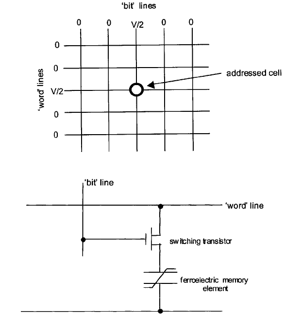
The principle on which a computer memory is based is illustrated in Fig. 5.53.
The binary-coded information is stored in an array of cells addressed by
voltage pulses applied to the ‘word’ and ‘bit’ lines. The response of a particular
cell, measured by the associated electronic circuitry, determines its state.
Figure 5.53(a) indicates the situation for a ‘passive’ FeRAM (ferroelectric
random access memory). If the capacitor is in the þP state (say a ‘1’) and the
application of two V/2 voltages is sufficient to switch the polarization to the P
state, there is a resulting ‘large’ current pulse. However were the cell in the P
state (a ‘0’) then the current pulse would be very much smaller. If the state of the
cell is such that the polarization is switched then a follow-on pulse must be
applied to return it to its original state.
In practice there are complications because the ferroelectric elements do not
have a sufficiently well defined switching voltage. This can lead to unintentional
switching of elements other than the one addressed and, consequently, to an
unacceptable error rate. The problem can be overcome by coupling each memory
element with a transistor which provides the sharply defined switching voltage.
In its simplest form each node of such an ‘active’ matrix would then take the
form shown in Fig. 5.53(b). In fact, for a variety of reasons associated with the
changes which occur in the physical properties of ferroelectrics with time, the
transistor-memory cell circuitry at each node is more complex than outlined
above, but the general principles are the same.
In the case of dynamic random access memories (DRAMs) the cell is a thin
film capacitor. The state of the cell (‘0’ or ‘1’) is read by the current pulse
following an addressing voltage pulse. Because the charge stored in the capacitor
leaks away in time (t ¼ RC) then, for the information to be retained it must be
periodically refreshed, the rate of leakage determining the necessary refresh
interval.
In the conventional DRAM the capacitor dielectric is SiO
2
(e
r
5) or a
combination of SiO
2
and Si
3
N
4
(‘ONO’ film) and is formed by controlled
oxidation or nitridation of the silicon crystal. It is necessary for the memory
capacitor to have a capacitance value of approximately 30 fF (i.e. 3010
15
F)
330 DIELECTRICS AND INSULATORS
* EEPROM, electrically erasable programmable read-only memory – a ‘FLASH’ memory.
and this places a lower limit on its size. A lower limit on the thickness of the
dielectric is necessary to retain adequate resistance to electrical breakdown
arising from ‘tunnelling’ currents. Capacitor size, and therefore component
density, can be reduced by increasing the permittivity of the dielectric. A
significant reduction in capacitor size could be achieved by replacing the silica
with Ta
2
O
5
(e
r
25) and this step seems likely in the foreseeable future. If a
‘ferroelectric’ capacitor (e
r
of order 10
2
to 10
3
) could be used then a bit density
increase of about ten-fold might be achieved. This is the stimulus for
considerable research and development effort, especially on SrTiO
3
(e
r
4 200)
and Ba
x
Sr
ð1xÞ
TiO
3
e.g. Ba
0.7
Sr
0.3
TiO
3
(e
r
4 300), the composition being chosen
so that the material is in the paraelectric phase at room temperature.
For FeRAMs materials attracting interest are PbZr
ð1xÞ
Ti
x
O
3
(with x 0:6)
and the Aurivillius layer-structured perovskite, SrBi
2
Ta
2
O
9
(SBT).
HIGH-PERMITTIVITY CERAMICS 331
Fig. 5.53 Schematic of FeRAM matrix: (a) a matrix of memory cells (b) each memory cell
coupled with a switching transistor to more closely define the threshold switching voltage.
(a)
(b)